HAL Id: hal-02013554
https://hal.archives-ouvertes.fr/hal-02013554
Submitted on 11 Feb 2019
HAL is a multi-disciplinary open access
archive for the deposit and dissemination of
sci-entific research documents, whether they are
pub-lished or not. The documents may come from
teaching and research institutions in France or
abroad, or from public or private research centers.
L’archive ouverte pluridisciplinaire HAL, est
destinée au dépôt et à la diffusion de documents
scientifiques de niveau recherche, publiés ou non,
émanant des établissements d’enseignement et de
recherche français ou étrangers, des laboratoires
publics ou privés.
Overvoltage at motor terminals in SiC-based PWM
drives
Bouazza Taghia, Bernardo Cougo, Hubert Piquet, David Malec, Antoine
Belinger, Jean-Pierre Carayon
To cite this version:
Bouazza Taghia, Bernardo Cougo, Hubert Piquet, David Malec, Antoine Belinger, et al.. Overvoltage
at motor terminals in SiC-based PWM drives. Mathematics and Computers in Simulation, Elsevier,
2018, 158, pp.264-240. �10.1016/j.matcom.2018.09.009�. �hal-02013554�
OATAO is an open access repository that collects the work of Toulouse
researchers and makes it freely available over the web where possible
Any correspondence concerning this service should be sent
to the repository administrator:
[email protected]
This is an author’s version published in:
http://oatao.univ-toulouse.fr/21388
To cite this version:
Taghia, Bouazza and Cougo, Bernardo and Piquet, Hubert
and Malec, David and Belinger, Antoine and Carayon,
Jean-Pierre Overvoltage at motor terminals in SiC-based PWM
drives. (2018) Mathematics and Computers in Simulation,
158. 264-240. ISSN 0378-4754
Official URL:
https://doi.org/10.1016/j.matcom.2018.09.009
Overvoltage
at motor terminals in SiC-based PWM drives
Bouazza
Taghia
a,b,∗,
Bernardo Cougo
a,
Hubert Piquet
b,
David Malec
b,
Antoine Belinger
b,
Jean-Pierre
Carayon
aaIRT Saint-Exupéry, CS34436, 3 Rue Tarfaya, 31400 Toulouse, France
bLAPLACE, Université de Toulouse, CNRS, INPT, UPS, 2 rue Charles Camichel, 31071 Toulouse, France
Abstract
Key points in the development of More Electrical Aircraft (MEA) are currently DC power distribution in higher voltage levels (540 V) and the use of disruptive technology such as Wide BandGap (WBG) semiconductors in power inverters. Using WBG components (SiC and GaN) increases the power converter mass density. However, fast switching of WBG components (tens of kV/µs) induces voltage transient overshoots due to parasitic elements within the inverter. In addition, propagation and reflection phenomena along the harness connected to this inverter, even for small lengths, cause a significant voltage overshoot across the loads. Such overvoltage in Adjustable Speed Drives (ASD: association of inverter, harness and motor) supplied by the new HVDC 540 V aeronautical network could be fatal for the Electrical Insulation System (EIS). This paper proposes a fast and accurate modeling methodology to predict transient overvoltage; it allows us to analyze the impact of SiC inverter technology on overvoltage at motor terminals.
Keywords: Overvoltage; Frequency modeling; SiC inverter; Adjustable Speed Drives (ASD); More Electrical Aircraft (MEA)
1. Introduction
1.1. Background: More Electrical Aircraft (MEA)
Currently, trends in modern aircrafts address the progressive replacement of hydraulic and pneumatic systems by electrical ones [31], Indeed, the electrical systems allow a better energetic efficiency: controlled generation, efficient distribution and better flexibility. In addition, the electric systems offer more faults detection facilities and better possibilities for reconfigurations, which allows drastic reductions in maintenance costs. In order to effectively respond
∗
Corresponding author at: IRT Saint-Exup´ery, CS34436, 3 Rue Tarfaya, 31400 Toulouse, France.
E-mail addresses: [email protected](B. Taghia), [email protected](H. Piquet). https://doi.org/10.1016/j.matcom.2018.09.009
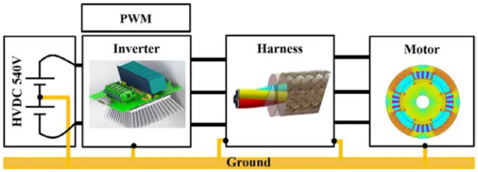
Fig. 1. Adjustable Speed Drive (ASD) for aeronautical application.
to the growing need in electrical energy, the voltage level aboard new aircraft generations has grown from 115VAC to 230VAC. This has given rise to a new high voltage DC bus (HVDC) of +/−270 V instead of classical +270 V.
Wide Bandgap (WBG) semiconductor technologies (Silicon Carbide—SiC, and Gallium Nitride—GaN) are
currently under evaluation to be used in converters for Adjustable Speed Drives in MEA (Fig. 1). These inverters
can be placed close to the motors or at a significant distance, which is usually the case when the motor is located in the wings and the converter in a pressurized area. Power cables usually called “harness” ensure the connection between inverters and motors. In ASD with cable of a few meters, high transient overvoltage at the motor terminals
can appear, which are even increased by the use of fast WBG semiconductors, such as SiC MOSFETs [33].
These transient overvoltages along the harness, combined with aeronautical operating constraints, such as low pressure and high temperature, can be fatal for the Electrical Insulation System (EIS). Its lifetime can be reduced by partial discharges and breakdown [7].
This paper presents a methodology aiming to accurately estimate overvoltage at the motor terminals caused by the association of fast switching of SiC inverter and the cable. In order to use our model in design tools, fast calculation is a desired criterion for quick evaluation of overvoltages at each design iteration.
1.2. Overvoltage in PWM Adjustable Speed Drives (ASD)
Since the beginning of the 20th century, the problem of transient overvoltage has been particularly addressed in the field of electric power transport. It is caused in particular by switching of breakers and by lightning aggression. Since the emergence of IGBTs in the late 1980s, this problem has started to be addressed in relation to ASD [29,36].
The relative fast IGBT switching and the difference between the harness characteristic impedance and its two termination impedances (inverter’s and/or motor’s one), called an “impedance mismatch”, causes the propagation and reflection phenomena along the harness. As consequence, an overvoltage at motor terminals appears after each inverter
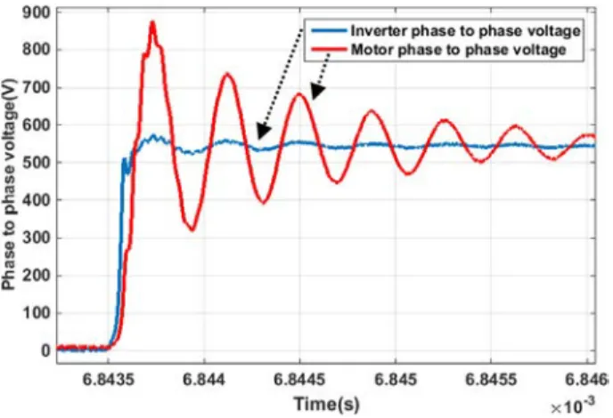
switching.Fig. 2shows an example of overvoltage measured on aeronautical ASD fed by HVDC 540 V network. As
shown inFig. 3, overvoltage is strongly related to the cable characteristics (construction and length) as well as to the speed (dv/dt) of inverter switching [20].
Overvoltage caused by one inverter voltage pulse does not exceed twice the DC bus voltage. This is called “overvoltage less than 2 pu”. Overvoltage greater than 2 pu may exist: it is caused by inverter polarity reversal [20] or by two pulses close one to the other in the output voltage of the inverter [2,20,33].
Several works [6,10,24,26,29] highlight the harmful impact of repeated transient overvoltage on the EIS of motor fed by fast inverter. Passive [16,17,19,25] and active [21,40] filters at the inverter output or at the motor input have been proposed to mitigate overvoltage at motor terminals. In addition, specific PWM control strategies have been proposed to avoid overvoltage greater than 2 pu [11,20,34].
Recent works on overvoltage topic address: – Optimization of filtering solutions [17].
– Influence of fast semiconductor technologies (such as SiC) on motor overvoltage [15,39]. – Analytical modeling of overvoltage for rapid pre-design purposes [8,19,30].
Fig. 2. Example of voltage measurement on aeronautical ASD during a switching instant : AC motor + 2 m harness fed by IGBT inverter (risetime = 50 ns).
Fig. 3. Motor terminal voltage for uncharged cable. Source:Extracted from [20].
1.3. Brief state of art of electromagnetic transient modeling
ASD is generally a three-phase system and is usually simplified to an equivalent two-phase system [3,20]. Indeed, it is assumed that the inverter modulator only switches one leg inverter at a time. Then, for the case of three-phase inverter with three legs, there are always two parallel legs of inverter in steady state with a return third leg that
is switched. According to works [3,20] using this assumption, the modeling by an equivalent two-phase line gives
satisfactory results. This assumption is adopted in this paper.
Historically, traveling-waves problems are studied graphically using the lattice diagram. This method is easily applicable to uniform and lossless transmission lines. It considers a reflection coefficient at each cable termination [5]. The inverter coefficient Γi nvis defined by Eq.(1)and that of the machine Γmot is defined by Eq.(2), where:
• Zcis the cable characteristic impedance;
• Zi nvis the inverter output impedance;
Γi nv= Zi nv−Zc Zi nv+Zc (1) Γmot = Zmot −Zc Zmot +Zc (2) Under assumption of real and constant reflection coefficients, analytical formulations of overvoltage at motor’s terminal can be established [4,30,35]. This allows a rapid analysis of overvoltage for design purposes. Moreover, model accuracy can be highly affected if the inductive and capacitive nature in inverter and/or in motor is neglected.
To overcome this limit, models with R, L and C lumped parameter can be used [32,37]. In this case, the propagation effect is taken into account by the cascading of several electrically short cable segments (wavelength much greater than the length of the cable segment). Moreover, the frequency effects (skin and proximity effects) can be taken into account by using a ladder circuit network [38]. By choosing a sufficiently large number of lumped elements, this method accurately represents the propagation effects. In addition, these models can be easily used in circuit simulation software such as SPICE, but their calculation time is excessive.
The method called “MoC: Method of Characteristics” is the compromise of the two previous ones [9,12,13].
It has been implemented since the 1960s in the Electro-Magnetic Transient Program (EMTP c⃝). It consists of
an exact solution of telegraphist equations for a lossless transmission line with distributed parameters. Losses are taken into account using lumped resistive elements. The generalized MoC uses the convolution product and macro-modeling techniques to take into account the frequency dispersion and the distributed nature of transmission line parameters [14,22]. MoC does not use the reflection coefficients and it can be implemented in circuit software.
All the works mentioned above use a time-based resolution. This has the advantage to easily take into account the time varying behavior such as the switching of the components used in power inverter: transistors and diodes. However, the iterative nature of time-based resolution and the use of small computation step (about nanoseconds for a hundreds megahertz frequency range requested to accurately describe the fast transients related to overvoltages) causes excessive computation time. Therefore, the time-based resolution is not adapted to the system pre-design.
Unlike the work of the state of the art, we propose in this paper a frequency modeling methodology to study transients, especially overvoltage. The convolution product used in the time domain becomes a simple product in the frequency domain. For linear systems, just one simple product of the spectrum of the input signals and the transfer function of the system is necessary. It can even be done by a parallel computation because the spectral components are independent. Globally, the frequency resolution is at least 6 times faster for our ASD studied problem (based
on comparison between our model and the MoC model implemented in Simscape toolbox of Matlab-Simulink⃝R
software). Moreover, telegraphists equations accept an exact solution in the frequency domain, thus no approximation is to be made for propagation, reflection, frequency dispersion and losses. The only limitation of frequency modeling comes with time-varying behavior of inverter. For this purpose, we propose in this paper an accurate linear equivalent model of SiC inverter. Very good agreement is observed with respect to measurements.
2. Transient overvoltage modeling 2.1. Cable modeling
2.1.1. Frequency transmission line modeling
Transmission line theory considers the basic and the most important assumption: the Transverse Electro-Magnetic (TEM) mode of propagation or quasi-TEM along the line. This is valid as long as the transversal dimensions of a harness (cross-section of cables and distances between them) are smaller than one-fourth of the shortest wavelengthλ
involved in the wave propagation (λ = ϑ/f = 3 m for wave with maximal frequency f = 100 MHz and propagates
at light velocityϑ = 3 · 108 m/s). Transmission line theory was successfully used to characterize lossy and/or
inhomogeneous structures into the gigahertz frequency range [27]. Overvoltage in ASD oscillates at some megahertz,
so, the transmission line theory is largely valid for our case study.
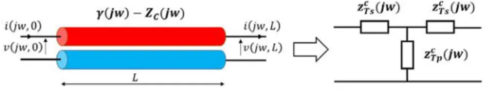
A cable with length equal to L is described by its A BC Dc chain-parameter matrix (Eqs.(3)–(5)). The A BC Dc
matrix is obtained from an exact mathematical solution of the two-conductor propagation equations [28]. The cable
model is characterized by its primary parameters: R LC G( jw) and by its secondary parameters: propagation function
Fig. 4. From two-conductor transmission line to frequency-based equivalent T circuit model of the two-conductor transmission line.
frequency. The R LC G parameters are global parameters of the cable; they depend on the self and mutual elements between different conductors. For the case of two conductors, R L formulations are given in [33].
( v ( jw, L) i( jw, L) ) =A BC Dc (v( jw, 0) i( jw, 0) ) =( Ac Bc Cc Dc ) ( v ( jw, 0) i( jw, 0) ) (3) where: ⎧ ⎪ ⎪ ⎨ ⎪ ⎪ ⎩ Ac=cosh(γc( jw) L) Bc= −Zcsinh(γc( jw) L) Cc= −sinh(γc( jw) L) /Zc( jw) Dc=cosh(γc( jw) L) (4) {γc( jw) = √(R ( jw) + jwL ( jw)) (G ( jw) + jwC ( jw)) Zc( jw) = √(R ( jw) + jwL ( jw)) / (G ( jw) + jwC ( jw)) (5) To facilitate the cable model interconnection to its termination models (inverter, motor, filter, measurement probes),
we propose to reformulate the exact solution of telegraphist’s equations(3) to establish an exact T circuit model
(Fig. 4) Eq.(6). {zc T p= −C −1 c =Zc/ sinh (γc( jw) L) zcT s =Cc−1(1 − Dc) = (cosh (γc( jw) L) − 1)Zc/ sinh (γc( jw) L) (6) Note that, in the modeling presented above, the propagation effect due to cable is taken into account thanks to the
frequency dependence of T circuit model parameters Eq.(6).
2.1.2. Per unit RLCG parameter calculation
There are three main methods to obtain R LC G parameters [28]:
1. Analytical method: Consisting of an exact solution of Maxwell’s equations. This is possible for transmission line structures with canonical conductor’s geometry (round or square) inserted in a homogeneous medium (air, dielectric). When exact solution exists, they are fast and accurate. Otherwise, approximations must be made, which can affect the accuracy.
2. Numerical method: Consisting of 2D/3D discretization of Maxwell’s equations to provide an approximate solution. The mesh fineness is chosen to satisfy a trade-off between the calculation time and the accuracy. 3. Experimental method: A well-done measurement take into account all the physical phenomena that occur in the
cable. To avoid measurement errors, many precautions must be taken into account, for example: good calibration and good connections between the test instrument and the device under test. This method does not require a knowledge about physical construction of the cable. It is generally used at the end of the design process to validate theoretical prediction (analytical or numerical methods).
As a result of TEM assumption, we can determine the per-unit-length resistance, inductance, capacitance and conductance by using only static field analysis methods in the transverse plane [28]. In this paper we propose to use a
2D numerical method implemented in FEMM software [23] driven by MATLAB software as illustrated inFig. 5. This
choice is in our opinion a very good trade-off between accuracy and calculation time. Parameters R L are obtained by the resolution of a quasi-magneto-static problem, while parameters C G are calculated by solving an electrostatic problem. Note that the calculation of R L parameters depends strongly on the mesh fineness. This simulation parameter
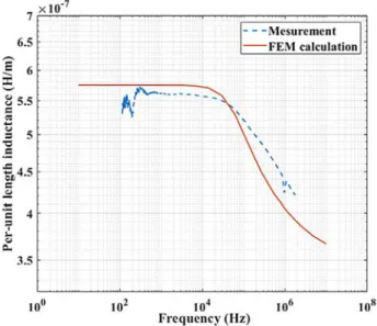
Fig. 7. Per-unit length inductance result of CF-AWG18-EN2267- 010A two cables.
Fig. 8. Per-unit length capacitance result of CF-AWG18-EN2267- 010A two cables.
2.2. SiC inverter modeling
One of the advantages of using SiC components in inverters is that they switch very fast and produce low losses. This reduces the need of cooling and thus the inverter weight. However, as shown by experimental characterization results (Fig. 10), the higher the dv/dt (modified by the gate resistance in this example), the lower switching losses but a higher overshoot of voltage ringing. In fact, very fast switching of a SiC inverter generates very complex resonance
phenomena (Fig. 11) which depends on several parameters: mainly the power modules parasitics (loop inductance,
semiconductor output capacitance) but also the output current Ii nverter and the DC bus voltage Vdcas well as if the
transistor is turning ON or OFF.
In terms of modeling, the inverter is a non-linear component according to current and voltage. Therefore, it cannot be directly simulated in frequency domain. Its behavior is often linearized by modeling its switching behavior by an
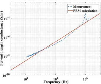
Fig. 9. Per-unit length conductance result of CF-AWG18-EN2267- 010A two cables.
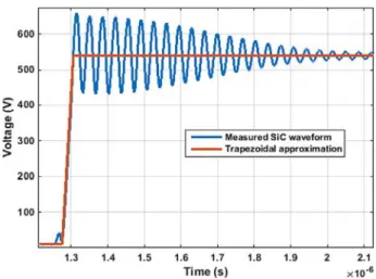
Fig. 10. Example of relationship between switching energies and (a) switching speed and (b) overshoot. These values were experimentally obtained for different gate resistances Rgat Vdc=540V and Ii nverter=50A, for CAS100H12AM1 SiC CREE module [33].
ideal trapezoidal source voltage, as illustrated byFig. 11, which is very different from an actual switching waveform of a SiC MOSFET, as shown in this figure.
To take into account the contribution of a SiC inverter ringing in the overvoltage at the motor terminals, we propose to consider an inverter model, as illustrated byFig. 12, composed of:
• Trapezoidal source voltage vi nv: Its dv/dt depends mainly on the gate resistance, the gate–source control
voltage, the DC supply voltage and the switched output current.
• Output capacitor cout: This parameter depends on the intrinsic parasitic capacitance of the SiC MOSFET
component. In this paper, we consider cout = coss. The coss capacitance is provided in the manufacturer’s
datasheet. Although it depends on the voltage across the component, in our model we consider a constant value, which is the one at the DC bus voltage.
• Loop impedance zloop=rloop+jlloopw: This undesirable parameter is caused by the electronic integration of
Fig. 11. Trapezoidal approximation of SiC inverter waveform.
Fig. 12. SiC inverter frequency model.
Table 1
Typical value of the motor impedance [18].
Motor power (kW) zmot()
<3.7 2000–5000
90 800
355 400
ringing frequency fr i ngi ngusing the following relation:
lloop=1/(cout·(2 · pi · fr i ngi ng
)2
) (7)
As a first approximation, the resistance rloop is considered equal to 2 · RD Son(two switching cells), the RD Son
resistance is provided in the manufacturer’s datasheet. If it is necessary, the resistance value can be adjusted so that the damping time will match the experimental one.
2.3. Motor modeling
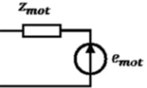
The motor is modeled as a back electromotive force (BEMF) emot with series impedance zmot (Fig. 13). A typical
Fig. 13. Circuit model of the motor.
Parameter zmot is frequency dependent and could greatly affect the overvoltage mechanism. However, in this paper
we focus only on the interaction between the inverter and the cable, thus we will assume in the following that zmot is
real and is higher than 5000.
2.4. Model resolution in frequency domain
Given the circuit modeling of different parts explained above, the whole ASD model can be easily assembled as shown inFig. 14. Note that the impedances of the probes used to measure voltage and current can be taken into account in this approach. Also, models of an eventual hardware filters at terminations of harness can be also easily added.
This circuit can be solved by the traditional nodal analysis by applying Kirchhoff’s voltage law (KVL) and
Kirchhoff’s current law (KCL). Moreover, to get faster calculation, analytical expressions (Eq.(8) and Eq.(9)) of
both inverter voltage Vi nverter and motor voltage Vmot orare established.
Vi nverter =(emot ·zT p·zloop·zout+2 ·vi nv·zT p·zT s·zout+vi nv·z2T s·zout+vi nv
·zT p·zmot·zout+vi nv·zT s·zmot·zout)/(2 · zT p·zT s·zloop+z2T s
·zloop+2 · zT p·zT s·zout+z2T s·zout+zT p·zloop·zmot +zT s ·zloop
·zmot +zT p·zloop·zout+zT s·zloop·zout +zT p·zmot·zout+zT s
·zmot ·zout+zloop·zmot·zout) (8)
Vmot or=(2 · emot·zT p·zT s·zloop+emot ·z2T s·zloop+2 · emot ·zT p·zT s·zout
+emot·z2T s ·zout+emot ·zT p·zloop·zout+emot ·zT s·zloop·zout
+vi nv·zT p·zmot ·zout)/(2 · zT p·zT s ·zloop+z2T s·zloop+2 · zT p
·zT s ·zout+z2T s·zout+zT p·zloop·zmot+zT s·zloop·zmot +zT p
·zloop·zout+zT s·zloop·zout+zT p·zmot ·zout+zT s·zmot·zout
+zloop·zmot·zout) (9)
The frequency resolution is implemented in Matlab software and is done in three steps: 1. Calculation of the input parameters of the model:
• Inverter parameters: spectrum of the trapezoidal voltage:F F T (vi nv), zloopand cout.
• Cable parameters: R LC G( jw) for the whole frequency range of F FT (vi nv).
• Motor parameters: spectrum of the motor BEMF: F F T (emot) and zmot.
2. Frequency calculation of voltage across inverter Vi nverterand that across motor terminals Vmot orin the frequency
band of interest.
3. Calculation of the time-based waveform by applying the Inverse Fast Fourier transform: I F F T (Vi nverter) and
I F F T(Vmot or).
Note that this approach allows us to easily take into account frequency effects such as skin and proximity effects on the model parameters. In the next session, this model is used to study the impact of fast switching and of cable length on overvoltage phenomena at motor terminals.
Fig. 14. Proposed frequency model of ASD. Circuit parameters can be frequency dependant.
Fig. 15. Trapezoidal approximation of SiC inverter output waveforms for different Rgat Vdc=540 V and Ii nverter=50 A, based on experimental results.
3. Overvoltage vs. SiC dv/dt and harness length
As said before, overvoltage at motor’s terminals is strongly related to harness length and also to inverter output
voltage waveform during the switching time (related to dv/dt). In the following, we propose a parametric study of
the overvoltage as a function of these two parameters.
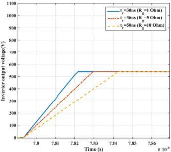
In this section, the inverter is approximated by a trapezoidal source voltage (the inverter internal impedances are neglected).Fig. 15shows an example of the rising edge of a trapezoidal voltage waveform at the output of a converter.
The dv/dt of each curve corresponds to measurements on SiC MOSFET at Vdc=540 V (Fig. 10), for three different
gate resistances Rg (1, 5 and 10 ).
Results presented below use R LC G harness parameters calculated in Section2.1.2. For simplicity and for the
reasons given in Section2.3, we represent the motor by a constant resistance : Zmot or =5000.
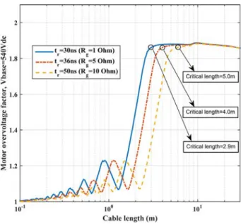
The developed frequency model is used to calculate the voltage waveform at motor terminals caused by trapezoidal inverter waveforms ofFig. 15. Results for harness length of 3 m are shown inFig. 16.
When changing Rgfrom 10 to 1 , the inverter rise time decreases from 50 ns to 30 ns and the maximum voltage
at the motor terminals increases from 715 V to 1000 V.
To study the influence of harness length on overvoltage at motor terminals, we calculate the maximal value of
motor overvoltage caused by trapezoidal voltage waveforms ofFig. 15 at each harness length. Results shown in
Fig. 17, qualitatively, are similar to the trends proposed in the EIC standard 60034-18-41 (Fig. 18). Quantitatively, our result is complimentary to that of EIC standard in terms of the studied rise times. In fact, inFig. 17, we use a measured
Fig. 16. Overvoltage at motor terminals obtained by simulation using trapezoidal inverter waveforms ofFig. 15for different Rgand cable length
of L = 3 m.
Fig. 17. Overvoltage ratio at motor terminals for different harness lengths, obtained by simulation using trapezoidal inverter waveforms.
rise time (from tr = 30 ns to tr = 50 ns) on CAS100H12AM1 SiC CREE module [33], whileFig. 18proposes a
study for trhigher than 50 ns, which is representative of fast IGBT inverter performances.
It is known that overvoltage caused by a single inverter rising edge increases with respect to the harness length. Its
maximal value, which does not exceed a double of DC voltage value (overvoltage < 2 pu), is achieved at the
so-called critical cable length (Figs. 17and18). For harness lengths greater than the critical cable length, the overvoltage value decreases slightly as a function of harness length due to losses. But it remains fairly close to 2 pu for aeronautical
harness length which is supposed up to 30 m. For fast IGBT with tr =50 ns, a critical length is around 5 m. While,
it is around 3 m for SiC inverter with rise time equal to 30 ns. Because of losses, the overvoltage ratio calculated by our model for the giving harness is less than 1.9 pu. Indeed, our model accurately takes into account distributed losses along the harness.
Fig. 18. Overvoltage ratio in function of harness length, proposed in EIC Standard (60034-18-41).
In terms of power converter design, as shown inFig. 17, increasing the gate resistance Rg is potentially a very
simple solution, which would significantly reduce motor overvoltage for relatively small harness lengths (<5 m).
Especially for aircraft applications where the length of the harness varies from a few centimeters to a few tenths of meters. The drawback of increasing Rgis that switching losses also increase. As we can see inFig. 10, when changing
Rg from 1 to 10 , the maximum voltage at the motor terminals decreases from 1000 V to 715 V. However, the
total energy (turn-on + turn-off) increases from around 930 to 2850 µJ (3 times higher switching losses). Therefore, to ensure at same time better inverter energy efficiency and the EIS reliability, a trade-off between losses and transient overvoltage must be considered right from the design step.
The used trapezoidal waveform assumption considers the inverter as a perfect voltage source: in other words, the dynamics of its output voltage is not affected by the inverter’s load (harness + motor). This is valid for slow inverters or for fast inverters with an optimal integration, which reduce their parasitic elements (especially the loop inductance). In the next section, we propose a study of overvoltage taking into account the internal parasitic elements of inverter. 4. Overvoltage vs. SiC ringing and harness length
The output inverter waveform cannot be actually considered as a trapezoidal waveform such as the ones ofFig. 15. The very fast switching of a SiC inverter generates complex ringing phenomena. To study the impact of SiC inverter voltage waveform on transient overvoltage, we carried out experimental investigations using a full-bridge SiC inverter based on CMF20120D components (from manufacturer CREE) connected to the two parallel aeronautical cables
(CF-AWG18-EN2267-010A) characterized in Section2.1.2. The experimental converter board is shown inFig. 19as
well as a representation of the cables connected to this converter. No load is connected, which is a worst case in terms of reflection on the load side.
4.1. Inverter model and complete system simulation
The behavioral SiC inverter model described in Section2.2is used in this last section. To identify its parameters we
use an association of SiC inverter and a long harness of 18.7 m. With this length, the two transient phenomena: SiC
inverter ringing and the harness voltage oscillation are relatively decoupled. In fact, as shown inFig. 20, the harness
voltage oscillation frequency is around 2.25 MHz and the voltage inverter ringing frequency is around 25.5 MHz.
By using:
• The dv/dt and the ringing frequency of inverter voltage from the experimental measurements ofFig. 20;
• The proposed identification methodology described in Section2.2;
• And the manufacturer datasheet of CMF20120D component.
Table 2
Identified parameters of inverter behavioral model.
Parameter Value
dv/dt 8.75 kV/µs
cout=coss 350 pF
lloop=1/(cout · (2 · pi · fr i ngi ng
)2
) 110 nH
rloop(≈ 2 · RD Son) 0.16
Fig. 19. Test Bench used to study the effect of SiC inverter ringing on harness overvoltage.
Fig. 20. Overvoltage caused by SiC inverter feeding a long CF-AWG18 harness of 18.7 m, for Vdc = 70 V, Rg = 10 and Vgs = 24 V.
By using those inverter parameters, the harness parameters presented in2.1.2and the developed frequency model in
2.4, we can calculate the voltage waveforms at inverter output and at harness output. Results are presented inFig. 20; there is a very good agreement (less than 5% difference) between experimental and simulated waveforms.
Fig. 21. Overvoltage caused by SiC inverter feeding a short CF-AWG18 harness of 2.3 m, for Vdc=70dc, Rg = 10 and Vgs = 24 V.
4.2. Overvoltage caused by inverter ringing
Before using our model to study the effect of inverter ringing on harness overvoltage, we propose to check the model by an additional configuration, which is different of that used to identify the inverter behavioral model parameters. We choose a relatively short cable of 2.3 m. At this length, the harness resonance frequency is close to
the inverter ringing frequency at V dc = 70 V. Results are presented inFig. 21; there is a good agreement between
experimental and simulated waveforms at the output of harness.
Note that the inverter voltage is no longer a sinusoidal damped waveform as inFig. 20. In this case, there is an interaction between the two oscillatory phenomena: inverter ringing and harness traveling-waves. A slight modeling error can be observed during the damping phase. However, we highlight that the first oscillation is not affected by the interactions between the inverter and the harness and recall that the objective of our study is to predict the maximal voltage that could potentially lead to partial discharges. Our model gives this information in a precise way (<5% difference).
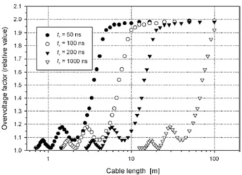
We can now consider that the model of the SiC inverter and CF-AWG18 harness is valid. We use it to calculate the maximum voltage at the output of the harness for different cable lengths taking into account the ringing behavior of the SiC inverter. Results are presented inFig. 22(solid red plot).
It is shown in the previous section that under the trapezoidal waveform assumption, overvoltage remains under 2 pu (dashed blue plot inFig. 22). Moreover, in literature, overvoltage caused by a single rising edge is conventionally classified as overvoltage lower than 2 pu. However, as clearly demonstrated by experimental test and simulation (stars
and solid red plot inFig. 22), overvoltage caused by single rising edge with ringing phenomena can be greater than
2 pu. In fact, the overvoltage caused by the inverter ringing is amplified by the harness. Then, in the worst case, the maximal harness overvoltage could reach the double of the maximal output inverter ringing voltage. This is verified in
Fig. 21for a harness with short length (<3 m). By increasing harness length, the effect of inverter ringing on harness
overvoltage is greatly reduced due to harness lossesFig. 22.
5. Conclusion
In this paper, we propose a propagation frequency model providing fast and accurate simulation of overvoltage along the harness. Using this model and the experimental characterizations of a SiC inverter, a parametric study of the overvoltage at motor terminals versus SiC gate resistance Rgand harness length is presented.
For inverter without ringing phenomena, we show that the variation of the gate resistance Rg could be used to
Fig. 22. Overvoltage factor ratio in function of CF-AWG18 harness length by taking into account inverter ringing, for 2.3 m, for Vdc=70dc, Rg
=10 and Vgs = 24 V. (For interpretation of the references to color in this figure legend, the reader is referred to the web version of this article.)
losses and transient overvoltage must be realized. As example, for 3 m harness, by changing Rgfrom 1 to 10 ,
the maximum voltage at the motor terminals decreases from 1000 V to 715 V. However, the total energy (turn-on + turn-off) increases from around 930 to 2850 µJ (3 times higher switching losses).
For inverter with ringing phenomena, we presented original investigations based on experimental and simulation works. This allows us to identify harmful effects of the voltage ringing at the output of the SiC inverter, which could create high overvoltage (>3 pu) at short harness length; this kind of overvoltage is fatal for the low voltage electrical insulation system currently used in aeronautical system.
Acknowledgments
These studies are conducted as a part of the FIABILITE project led by the Institute of Technological Research Saint Exupery (Institut de Recherche Technologique Saint Exup´ery) in collaboration with LAPLACE laboratory, AIRBUS Group, SAFRAN Group, ZODIAC AEROSPACE, LIEBHERR AEROSPACE and AEROCONSEIL. The authors would like to thank all the project members for giving them permission to publish this work, their financial support and technical discussions.
References
[1] A. Agrawal, K. Lee, L. Scott, H. Fowles, Experimental characterization of multiconductor transmission lines in the frequency domain, IEEE Trans. Electromagn. Compat. EMC-21 (1) (1979) 20–27.
[2] S. Amarir, K. Al-Haddad, Mathematical analysis and experimental validation of transient over-voltage higher than 2 per unit along industrial ASDM long cables, in: 2008 IEEE Power Electronics Specialists Conference, 2008, pp. 1846–1851.
[3] S. Amarir, K. Al-Haddad, Over-voltages computation algorithm for motors fed from long cable PWM drives, in: Proc. Mediterr. Electrotech. Conf. - MELECON, 2008, pp. 554–559.
[4] S. Amarir, K. Al-Haddad, A new mathematical tool to investigate the influence of cable characteristics and IGBT fast switching on voltage transients and differential mode currents for PWM drives, Math. Comput. Simulation 81 (2) (2010) 180–193.
[5] L.O. Barthold, G.K. Carter, Digital traveling-wave solutions i-single-phase equivalents, Trans. Am. Inst. Electr. Eng. Part III Power Appar. Syst. 80 (3) (1961) 812–818.
[6] P. Bidan, T. Lebey, G. Montseny, J. Saint-Michel, Transient voltage distribution in inverter fed motor windings: experimental study and modeling, IEEE Trans. Power Electron. 16 (1) (2001) 92–100.
[7] T. Billard, C. Abadie, B. Taghia, Advanced partial discharge testing of 540V aeronautic motors fed by SiC inverter under altitude conditions, in: AeroTech Congress & Exhibition, 2017, p. 17.
[8] T. Billard, C. Abadie, B. Taghia, Non-Intrusive Partial Discharges Investigations on Aeronautic Motors, 2016. [9] F.H. Branin, Transient analysis of lossless transmission lines, Proc. IEEE 55 (11) (1967) 2012–2013.
[10] A. Cavallini, D. Fabiani, G. Montanari, Power electronics and electrical insulation systems Part 1: Phenomenology overview, IEEE Electr. Insul. Mag. 26 (3) (2010) 7–15.
[11] S. De Caro, S. Foti, T. Scimone, A. Testa, G. Scelba, M. Pulvirenti, S. Russo, Over-voltage mitigation on SiC based motor drives through an open end winding configuration, in: 2017 IEEE Energy Conversion Congress and Exposition, ECCE, 2017, pp. 4332–4337.
[12] H. Dommel, Digital computer solution of electromagnetic transients in single-and multiphase networks, IEEE Trans. Power Appar. Syst. PAS-88 (4) (1969) 388–399.
[13] H.W. Dommel, W.S. Meyer, Computation of electromagnetic transients, Proc. IEEE 62 (7) (1974) 983–993.
[14] B. Gustavsen, A. Semlyen, Rational approximation of frequency domain responses by vector fitting, IEEE Trans. Power Deliv. 14 (3) (1999) 1052–1061.
[15] J. He, H. Chen, R. Katebi, N. Weise, N.A.O. Demerdash, Mitigation of uneven surge voltage stress on stator windings of induction motors fed by SiC-MOSFET-based adjustable speed drives, in: 2017 IEEE International Electric Machines and Drives Conference, IEMDC, 2017, pp. 1–7.
[16] J. He, G.Y. Sizov, P. Zhang, N.A.O. Demerdash, A review of mitigation methods for overvoltage in long-cable-fed PWM AC drives, in: 2011 IEEE Energy Conversion Congress and Exposition, 2011 (1028348) pp. 2160–2166.
[17] M.K. Hussain, P. Gomez, Optimal filter tuning to minimize the transient overvoltages on machine windings fed by PWM inverters, in: 2017 North American Power Symposium, NAPS, 2017, pp. 1–6.
[18] IEC/TS 61800-8, Adjustable speed electrical power drive systems - Part 8 : Specification of voltage on the power interface, 2010.
[19] Y. Jiang, W. Wu, Y. He, H.S.-H. Chung, F. Blaabjerg, New passive filter design method for overvoltage suppression and bearing currents mitigation in a long cable based PWM inverter-fed motor drive system, IEEE Trans. Power Electron. 32 (10) (2017) 7882–7893.
[20] R.J. Kerkman, D. Leggate, G.L. Skibinski, Interaction of drive modulation and cable parameters on AC motor transients, IEEE Trans. Ind. Appl. 33 (3) (1997) 722–731.
[21] J. Korhonen, Active Inverter Output Filtering, Lappeenranta University of Technology, 2012.
[22] O.R. Leanos, Wideband Line/Cable Models for Real-Time and Off-Line Simulations of Electromagnetic Transients, (Thesis), 2013. [23] D. Meeker, Finite Element Method Magnetics (FEMM).
[24] M.J. Melfi, Low-Voltage PWM inverter-fed motor insulation issues, IEEE Trans. Ind. Appl. 42 (1) (2006) 128–133.
[25] A.F. Moreira, High frequency modeling for cable and induction motor over-voltage studies in long cable drives, in: IEEE Ind. Appl. Soc. 36th Annu. Meet. Chicago, Illinois, USA, 2001.
[26] A.F. Moreira, P.M. Santos, T.A. Lipo, G. Venkataraman, Filter networks for long cable drives and their influence on motor voltage distribution and common-mode currents, IEEE Trans. Ind. Electron. 52 (2) (2005) 515–522.
[27] C.R. Paul, Decoupling the multiconductor transmission line equations, IEEE Trans. Microw. Theory Tech. 44 (8) (1996) 1429–1440. [28] C.R. Paul, Analysis of Multiconductor Transmission Lines, second ed., 2008.
[29] E. Persson, Transient effects in application of PWM inverters to induction motors, IEEE Trans. Ind. Appl. 28 (5) (1992) 1095–1101. [30] G. Pietrini, D. Barater, C. Concari, M. Galea, C. Gerada, Closed-form approach for predicting overvoltage transients in cable-fed PWM motor
drives for MEA, in: 2016 IEEE Energy Conversion Congress and Exposition (ECCE), 2016, pp. 1–7.
[31] X. Roboam, New trends and challenges of electrical networks embedded in ‘more electrical aircraft, ’ in: 2011 IEEE International Symposium on Industrial Electronics, 2011, pp. 26–31.
[32] G. Skibinski, R. Tallam, R. Reese, B. Buchholz, R. Lukaszewski, Common Mode and Differential Mode Analysis of Three Phase Cables for PWM AC Drives, in: Conference Record of the 2006 IEEE Industry Applications Conference Forty-First IAS Annual Meeting, 2006, 2, pp. 880–888.
[33] B. Taghia, B. Cougo, H. Piquet, D. Malec, A. Belinger, J.P. Carayon, Advanced analysis of transient overvoltage in electromechanical chain fed by SiC inverter, in: ELECTRIMACS, 2017, p. 6.
[34] A. Videt, P. Le Moigne, N. Idir, P. Baudesson, J.-J. Franchaud, J. Ecrabey, Motor overvoltage limitation by means of a new EMI-reducing PWM strategy for three-level inverters, IEEE Trans. Ind. Appl. 45 (5) (2009) 1678–1687.
[35] A. von Jouanne, P.N. Enjeti, Design considerations for an inverter output filter to mitigate the effects of long motor leads in ASD applications, IEEE Trans. Ind. Appl. 33 (5) (1997) 1138–1145.
[36] A. von Jouanne, P. Enjeti, W. Gray, Application issues for PWM adjustable speed AC motor drives, IEEE Ind. Appl. Mag. 2 (5) (1996) 10–18. [37] L. Wang, C. Ngai-Man Ho, F. Canales, J. Jatskevich, High-frequency modeling of the long-cable-fed induction motor drive system using
TLM approach for predicting overvoltage transients, IEEE Trans. Power Electron. 25 (10) (2010) 2653–2664.
[38] Y. Weens, N. Idir, R. Bausiere, J.J. Franchaud, Modeling and simulation of unshielded and shielded energy cables in frequency and time domains, IEEE Trans. Magn. 42 (7) (2006) 1876–1882.
[39] P. Yi, P.K.S. Murthy, L. Wei, Performance evaluation of SiC MOSFETs with long power cable and induction motor, in: 2016 IEEE Energy Conversion Congress and Exposition, ECCE, 2016, pp. 1–7.
[40] K.K.-F. Yuen, H.S.-H. Chung, V.S.-P. Cheung, An active low-loss motor terminal filter for overvoltage suppression and common-mode current reduction, IEEE Trans. Power Electron. 27 (7) (2012) 3158–3172.