HAL Id: hal-01347354
https://hal.inria.fr/hal-01347354
Submitted on 20 Jul 2016
HAL is a multi-disciplinary open access
archive for the deposit and dissemination of
sci-entific research documents, whether they are
pub-lished or not. The documents may come from
teaching and research institutions in France or
abroad, or from public or private research centers.
L’archive ouverte pluridisciplinaire HAL, est
destinée au dépôt et à la diffusion de documents
scientifiques de niveau recherche, publiés ou non,
émanant des établissements d’enseignement et de
recherche français ou étrangers, des laboratoires
publics ou privés.
Loop Optimization in Presence of STT-MRAM Caches:
a Study of Performance-Energy Tradeoffs
Pierre-Yves Péneau, Rabab Bouziane, Abdoulaye Gamatié, Erven Rohou,
Florent Bruguier, Gilles Sassatelli, Lionel Torres, Sophiane Senni
To cite this version:
Pierre-Yves Péneau, Rabab Bouziane, Abdoulaye Gamatié, Erven Rohou, Florent Bruguier, et al..
Loop Optimization in Presence of STT-MRAM Caches: a Study of Performance-Energy Tradeoffs.
PATMOS: Power and Timing Modeling, Optimization and Simulation, Sep 2016, Bremen, Germany.
pp.162-169, �10.1109/PATMOS.2016.7833682�. �hal-01347354�
Loop Optimization in Presence of STT-MRAM
Caches: a Study of Performance-Energy Tradeoffs
Pierre-Yves P´eneau
∗, Rabab Bouziane
†, Abdoulaye Gamati´e
∗, Erven Rohou
†, Florent Bruguier
∗,
Gilles Sassatelli
∗, Lionel Torres
∗and Sophiane Senni
∗∗LIRMM, CNRS and University of Montpellier – email: [email protected] †Inria/IRISA – email: [email protected]
Abstract—Energy-efficiency is one of the most challenging design issues in both embedded and high-performance computing domains. The aim is to reduce as much as possible the energy consumption of considered systems while providing them with the best computing performance. Finding an adequate solution to this problem certainly requires a cross-disciplinary approach capable of addressing the energy/performance trade-off at differ-ent system design levels. In this paper, we presdiffer-ent an empirical impact analysis of the integration of Spin Transfer Torque Magnetic Random Access Memory (STT-MRAM) technologies in multicore architectures when applying some existing compiler optimizations. For that purpose, we use three well-established architecture and NVM evaluation tools: NVSim, gem5 and McPAT. Our results show that the integration of STT-MRAM at cache memory levels enables a significant reduction of the energy consumption (up to 24.2 % and 31 % on the considered multicore and monocore platforms respectively) while preserving the per-formance improvement provided by typical code optimizations. We also identify how the choice of the clock frequency impacts the relative efficiency of the considered memory technologies.
I. INTRODUCTION
In embedded computing, while systems power budget is con-fined to a few watts, the performance demand is growing. This comes from the continuous integration of new functionalities in these systems, e.g., in mobile computing. To address this demand, the number of cores has been increasing. In high-performance computing (HPC), supercomputers are expected to achieve 1018 floating-point operations per second within
a power budget of 20 MW [1] around 2020. With current technologies, such a supercomputer would require a power budget of at least 300 MW (i.e., the power budget of a European small-size city), calling for new design solutions. These observations from both embedded and HPC domains draw their convergence towards finding the best ratio between performance and power consumption, i.e., energy-efficiency [2]. Finding an adequate solution to this problem certainly requires a cross-disciplinary approach capable of adequately addressing the energy/performance trade-off in systems. Such approaches should focus at the same time on different sys-tem design levels, including typically application software, compilation, operating systems/runtime, hardware architecture and underlying circuit/technology. In this paper, we consider compilers optimization applied to programs that are executed on different architecture configurations by varying parameters such as core count and frequency level. In addition, an emerging
non-volatile memory (NVM) technology is combined with SRAM technology in the cache memory hierarchy of these architectures. We seamlessly combine suitable architecture simulation and technology evaluation tools in order to evaluate various system scenarios. This enables us to assess the synergistic impact of the multi-level design decisions on system performance and energy consumption. As in [3], we use the gem5 simulator [4] for performance evaluation, and NVSim [5] and McPAT [6] for estimating the energy respectively related to NVMs and the rest of the architecture.
Our contribution. We propose an empirical impact analysis about energy efficiency when integrating Spin Transfer Torque Magnetic Random Access Memory (STT-MRAM) technologies [7] in embedded multicore architectures, while applying loop nest optimization [8] to application code. Magnetic memories are considered as promising technologies that combine desirable properties such as good scalability, low leakage, low access time and high density. On the other hand, loop nest optimization has been extensively studied for decades to improve code quality w.r.t. its performance. However, current compilers are not tuned for NVM. Here, we focus on loop permutation and tiling, which have an important impact on the locality of memory accesses. The considered architecture scenarios rely on ARM Cortex-A15 cores. Our experiments show that loop optimizations combined with STT-MRAM provide up to 24.2 % and 31 % energy reduction without performance degradation, respectively compared to multicore and monocore architectures with full SRAM cache hierarchy. They also show that this gain depends on the correlation between the chosen memory technology and the operating frequency. To the best of our knowledge, this is the first study that attempts to explore such a multi-level design, which is central for the energy-efficiency challenge in modern computing systems.
Outline. Section II discusses related work. Then, Section III introduces two examples of loop nest optimizations. Section IV studies suitable architectural design choices for NVM usage. Section V uses these choices to explore the performance and energy trade-off resulting from the loop optimizations on a monocore platforms integrating STT-MRAM in cache hierarchy. Section VI extends the study to multicores by parallelizing the execution of the optimized code. Section VII summarizes the main insights gained from our empirical analysis. Finally, Section VIII concludes and draws perspectives.
II. RELATED WORK
We first review some relevant studies on architecture design where NVMs are taken into account. Then, further works that exploit NVMs through compiler optimizations are discussed. A. Architecture design based on NVMs
In [9], [10], authors consider hybrid L1 caches composed of both SRAM and STT-MRAM technologies at the same cache level. Write-intensive data blocks are stored in the SRAM banks to reduce the penalty of the STT-MRAM in terms of latency and dynamic energy. A solution is therefore proposed for reducing the overhead related intra-cache data migration between SRAM and STT-MRAM banks as this requires extra read and write operations. It relies on a compile-time analysis (in LLVM compiler) that detects the write intensity of data blocks stored in the stack and gives them a “caching preference”. Authors showed on the MiBench [11] benchmark that the overall cache access latency and the dynamic energy are respectively reduced by 12.1 % and 10.8 %. Another approach, named Software Dispatch[12], operates at both compiler and operating system levels. The compiler analyzes write-intensive data blocks in the heap in order to guide the hardware in the data migration in hybrid SRAM/STT-MRAM caches. They also focus on hybrid main memory in which virtual segments (code, heap, stack) have distinct access patterns. They apply a data flow analysis [13] at compile-time so that the memory allocator can address the access patterns identified during the analysis. They validated their approach by using HSPICE [14] and CACTI and by executing the SPLASH-2 and PARSEC benchmarks using the Simics simulator [15]. Reported results show performance and power improvements of 5 % and 9.8 % respectively.
While all above studies mainly focus on the hybrid nature of specific cache levels, the scope of our study is more general. Here, we aim at investigating the suitable multi-level design choices capable of providing good performance/energy trade-offs, by exploring the impact of a full integration of STT-MRAM at the different cache hierarchy levels on both single-core and multisingle-core architectures.
B. Compiler optimizations targeting NVM
Hundreds of optimization techniques have been developed over the past decades [8], [16]. Each optimization tries to im-prove performance by focusing on a particular aspect: removing spurious dependencies, eliminating redundant computations, improving usage of hardware resources, etc. A strong emphasis has been put on the most time-consuming aspects i.e. loop optimizations and optimizations for the cache hierarchy.
Regarding hybrid caches, numerous approaches tried to mitigate the overhead of NVM writing operations. Reducing the number of writes activities on NVMs had been the most studied approach to overcome this drawback. Cache performance is dependant on the history of memory access. Therefore, data placement or data allocation is extremely important to make an hybrid architecture successful. Authors in [17] proposed an approach that aim to reduce write activities on NVM through register allocation technique to minimize the number of store
instructions. Register allocation is the process of assigning a program variables onto a small number of physical registers. The objective is to keep variables values in registers as long as possible, because accessing them is faster than memory. In the best case, a variable’s value would be kept in a register during its lifetime and would not need be written back to memory. In this approach, the authors extended the traditional register allocation algorithms that do not differentiate read and write activities and do not try to minimize writes through other methods, with re-computation to reduce write/stores operations. It consists of re-computing some variables that have to be spilled to memory to reduce writes as much as possible, if the cost of re-computing is less than the cost of spilling to memory. The cost is computed based on the execution frequency and the easiness of re-computation.
Another approach to alleviate the cost of write operations is to relax its non-volatility property. In [18], authors brought forward the retention time of NVMs. The retention time is the time throughout data is retained stored. As the retention time decreases, write current and write energy consumption are reduced. However, reducing retention time may not be sufficient to keep long living data in cache blocks, and can increase the number of stochastic errors. Consequently, to avoid losing data as a result of volatility, refresh schemes have been proposed. Refresh operations have also further overhead. Therefore, the new objective becomes to significantly reduce the number of refresh operations through re-arranging program data layout at compilation time.
In the current work, we investigate a few existing compilation techniques and analyze how they fit within an NVM-based architecture. Our future perspectives are to propose new energy-aware compilation techniques that are suitable for NVM technologies, particularly STT-MRAM.
III. CONSIDERED CODE OPTIMIZATIONS
Compiler optimizations are usually performed in order to improve performance, i.e. reduce execution time. They do so, for example, by eliminating redundancies, or decreasing the number of cache misses and branch mispredictions. In the sequel, we briefly discuss the current practice in modern compilers regarding program optimizations. Then, we introduce the two loop transformations used for illustrating our study. A. Practice in modern compilers
Modern compilers carry out dozens of optimizations that aim to increase instruction-level parallelism and improve data locality. Most of these optimizations apply loop restructuring. Loop transformations are particularly useful when the cache is the main bottleneck. Hence, performance-oriented compiler optimizations and memory energy consumption are interdepen-dent. The best performance optimizations may not lead to the best energy behavior in memory [19]. Yet, good optimizations for performance are in general energy-efficient, because they eliminate redundancy, and better manage registers, caches and memory. In turn, this can reduce the leakage power.
More concretely, the source code modification and restructur-ing enable a compiler to perform suitable transformations such as vectorization and parallelization, in order to better exploit cache hierarchy or to reduce power. Even if the majority of code transformations has shown prominent results, it is still difficult to choose the transformations that should be applied on a given program/code section and the order according to which they should be applied. This is known as phase-order problem [20]. This led to iterative compilation [21] which consists in generating multiple versions of the program code and choosing the best based on profiling on the considered hardware platform. In practice, this approach is too time-consuming due to the potentially large number of possible combinations. For this reason, existing solutions rely on heuristics or focus on a smaller set of transformations that can provide good results.
In the context of energy consumption, different loop opti-mizations have been evaluated individually and collectively, taking into consideration the trade-off between performance and energy with SRAM cache memories [22], [23], [24]. In this work, we focused on two transformations that heavily impact the locality of memory access: loop tiling and loop permutation, and we study their impact on performance and energy consumption in the presence of NVM, compared to a baseline scenarios with full SRAM cache memories.
B. Loop tiling and permutation
We consider the initial code extract1 described in Figure 1.
This code is a typical loop nest that performs a dense linear algebra computation called symmetric rank 2k update. It mainly performs multiplications and additions of the elements from two input matrices denoted by A and B. The result is stored into the unique output matrix C.
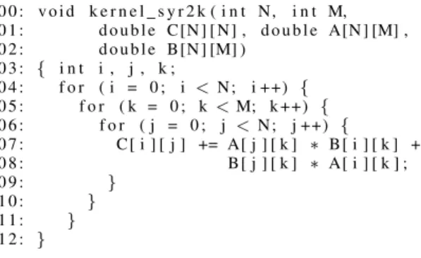
0 0 : v o i d k e r n e l s y r 2 k ( i n t N , i n t M, 0 1 : d o u b l e C [N ] [ N ] , d o u b l e A[N ] [M] , 0 2 : d o u b l e B [N ] [M] ) 0 3 : { i n t i , j , k ; 0 4 : f o r ( i = 0 ; i < N ; i ++) { 0 5 : f o r ( k = 0 ; k < M; k ++) { 0 6 : f o r ( j = 0 ; j < N ; j ++) { 0 7 : C [ i ] [ j ] += A[ j ] [ k ] ∗ B [ i ] [ k ] + 0 8 : B [ j ] [ k ] ∗ A[ i ] [ k ] ; 0 9 : } 1 0 : } 1 1 : } 1 2 : }
Fig. 1. Extract of modified syr2k code.
Note that this code is a modified version of an original version defined in the Polybench benchmark [25] devoted to numerical computations. The modifications are deliberately not optimized w.r.t. the loop index ordering. This is solved by applying one of the loop transformations considered here as illustrated in this paper.
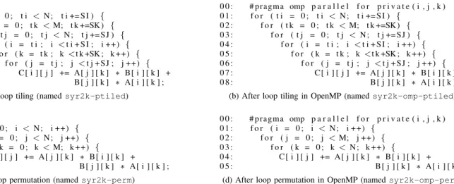
From the code extract specified in Figure 1, we derive four variants by applying loop tiling and permutation to the 1This code has been obtained from http://perso.ens-lyon.fr/tomofumi.yuki/
ejcp2015.
loop nest defined in the kernel_syr2k function. Both loop optimizations are considered in sequential and parallel versions of this function as shown in Figure 2.
Loop tiling splits the iteration space of a loop into smaller chunks or blocks, in such a way that the data used in the loop remains in the cache until it is reused. This leads to splitting large arrays into fine grain blocks, which in turn enables the accessed array elements to fit into the cache size. For a given loop, finding an optimal tile size is not trivial as this depends on loop accessed array regions and on the cache size of the target machine [26]. Figures 2a and 2b respectively denote the optimized sequential and parallel (by using OpenMP pragmas) codes resulting from loop tiling when applied to kernel_syr2kfunction. They are intended for single-core and multicore architectures respectively.
Loop permutation (or interchange) consists in exchanging the order of different iteration variables within a loop nest. It aims at improving the data locality by accessing the elements of a multidimensional array in an order according to which they are available in cache memory (the layout of arrays in C in row-major). Figures 2c and 2d feature respectively optimized sequential and parallel codes corresponding to kernel_syr2kfunction after loop permutation.
To measure the effect of considered optimizations, the execution time for the baseline version shown in Figure 1 must be relevant enough, i.e., not very small. Thus, we did an empirical analysis based on an Odroid-XU4 [27] board which integrates an Exynos-5422 System-on-Chip (SoC) [28]. This SoC contains two clusters of ARM cores, one with four Cortex-A7 and another with four Cortex-A15. For our experiments, we only used the latter. Given (M, N ) = (450, 450) as input parameter values, the execution time of syr2k is nearly 40 seconds, which is enough for measuring the optimization effects. For the tiling optimization, an exhaustive search yields 9 as the most efficient block size corresponding to the chosen input parameter values.
IV. IMPACT OFOPERATINGFREQUENCY ONCACHE
LATENCY
An important concern with NVMs is their related access latency when writing or reading data. The motivation of the current section is not to modify existing NVMs for better performance or lifetime, but to identify the relevant architectural parameters that have a significant impact on the efficient utilization of NVMs in a system-on-chip. In particular, we deal with the question about the choice of the suitable operating frequency at which data access should be considered in such a memory so as to minimize its latency penalty.
Let us consider the latency of memory operations, i.e. read/write, in terms of number of clock cycles. The duration, e.g. in second, of such cycles basically depends on the considered operating frequency. Higher frequencies trivially induce a shorter duration for a cycle while lower frequencies lead to a longer duration. For a given memory technology and a given cache configuration, two different frequencies lead to two different latencies in clock cycles for the same operation.
0 0 : f o r ( t i = 0 ; t i < N ; t i += S I ) { 0 1 : f o r ( t k = 0 ; t k < M; t k +=SK ) { 0 2 : f o r ( t j = 0 ; t j < N ; t j += SJ ) { 0 3 : f o r ( i = t i ; i < t i + S I ; i ++) { 0 4 : f o r ( k = t k ; k <t k +SK ; k ++) { 0 5 : f o r ( j = t j ; j < t j + SJ ; j ++) { 0 6 : C [ i ] [ j ] += A[ j ] [ k ] ∗ B [ i ] [ k ] + 0 7 : B [ j ] [ k ] ∗ A[ i ] [ k ] ;
(a) After loop tiling (named syr2k-ptiled)
0 0 : # pragma omp p a r a l l e l f o r p r i v a t e ( i , j , k ) 0 1 : f o r ( t i = 0 ; t i < N ; t i += S I ) { 0 2 : f o r ( t k = 0 ; t k < M; t k +=SK ) { 0 3 : f o r ( t j = 0 ; t j < N ; t j += SJ ) { 0 4 : f o r ( i = t i ; i < t i + S I ; i ++) { 0 5 : f o r ( k = t k ; k <t k +SK ; k ++) { 0 6 : f o r ( j = t j ; j < t j + SJ ; j ++) { 0 7 : C [ i ] [ j ] += A[ j ] [ k ] ∗ B [ i ] [ k ] + 0 8 : B [ j ] [ k ] ∗ A[ i ] [ k ] ;
(b) After loop tiling in OpenMP (named syr2k-omp-ptiled)
0 0 : f o r ( i = 0 ; i < N ; i ++) { 0 1 : f o r ( j = 0 ; j < N ; j ++) { 0 2 : f o r ( k = 0 ; k < M; k ++) { 0 3 : C [ i ] [ j ] += A[ j ] [ k ] ∗ B [ i ] [ k ] +
0 4 : B [ j ] [ k ] ∗ A[ i ] [ k ] ;
(c) After loop permutation (named syr2k-perm)
0 0 : # pragma omp p a r a l l e l f o r p r i v a t e ( i , j , k ) 0 1 : f o r ( i = 0 ; i < N ; i ++) { 0 2 : f o r ( j = 0 ; j < M; j ++) { 0 3 : f o r ( k = 0 ; k < N ; k ++) { 0 4 : C [ i ] [ j ] += A[ j ] [ k ] ∗ B [ i ] [ k ] + 0 5 : B [ j ] [ k ] ∗ A[ i ] [ k ] ;
(d) After loop permutation in OpenMP (named syr2k-omp-perm) Fig. 2. Evaluated loop optimization and parallelization.
Typically, let us consider a read duration of 2 ns for a cache. A frequency of 1.0 GHz provides a clock cycle of one nanosecond while at 2.0 GHz the duration of the clock cycle will be 0.5 nanosecond. This implies respective read operation latencies equal to 4 and 2 cycles. In the preliminary study presented below, we determine the latency of memory access in clock cycles for both SRAM and Spin Transfer Torque Magnetic Random Access Memory (STT-MRAM) depending on different operating frequencies with their associated memory operation duration.
A. Experimental setup
This study is conducted with NVSim [5], a circuit-level model for memory performance and area. Beyond the classical SRAM, it supports a large variety of NVMs, including STT-MRAM, PCRAM, ReRAM and NAND Flash. Its NVMs models have been validated against industrial prototypes. NVSim achieves within a reasonable time an estimation of electrical features of a complete memory chip, including read/write access duration in seconds, read/write access energy, and static power. It is used here to evaluate both SRAM and STT-MRAM caches. We set the suitable size, associativity and technology parameters. Most importantly, for two main reasons, we mainly focus on read operation latency. First, in the chosen scenario, the number of read operations is much larger than the number of write operations. Second, write latencies of STT-MRAM are an order of magnitude higher than the SRAM ones. Indeed the current STT-MRAM chips are not enough optimized to compete with SRAM caches regarding write latency. Yet, some ongoing efforts [29], [30] address this issue by suggesting new hardware mechanisms. This is not the case in the current work.
Our case study is a 32 KB 4-way associative L1 cache, manu-factured with 45 nm technology. We choose this parameter so as to reflect the state-of-the-art for STT-MRAM technologies [31]. We therefore compare this cache with a 45 nm SRAM cache.
The size and associativity values reflect the actual L1 cache in the Odroid-XU4 mentioned in Section III-B.
B. Results
The results of our NVSim-based evaluation scenarios are reported in Figure 3. In the ranges 0.1–0.5 GHz, and 0.8– 1.0 GHz, the read latencies of SRAM and NVM are identical. They are equal to 1 and 2 cycles respectively. In the other ranges, the read latencies differ. At 2.0 GHz, latencies are 3 and 4 cycles for SRAM and STT-MRAM respectively. It is important to notice that the results reported in Figure 3 are valid for a memory size of 32 KB. Some studies [32] show that for large size memories, in particular above a few hundreds of KBs, the read latency of SRAM becomes higher than that of STT-MRAM. STTMRAM SRAM R ea d L at en cy ( cy cl es ) 1 2 3 4 5 CPU Frequency (GHz) 0,2 0,4 0,6 0,8 1 1,2 1,4 1,6 1,8 2 2,2
Fig. 3. Evolution of the cache latency for read operation with different CPU frequencies
From these results, we choose a frequency that results in identical latencies for both memory technologies for a fair comparison in the next sections. Indeed, we observe that the
Read Write 32 KB L1 in SRAM 2 2 256 KB L2 in SRAM 6 6 2 MB L2 in SRAM 18 18 32 KB L1 in STT-MRAM 2 11 256 KB L2 in STT-MRAM 10 18 2 MB L2 in STT-MRAM 25 28 TABLE I
SRAMANDSTT-MRAMCACHE LATENCY IN CYCLES AT1.0 GHZ
impact of STT-MRAM on performance and energy consump-tion depends on the considered core operating frequencies, which lead to various memory operation latencies. To the best of our knowledge, no existing work addresses this central question.
Our CPU target is an ARM Cortex-A15 [33] – a powerful out-of-order CPU built for high performance computation – we opted for the maximum available frequency, i.e., 1.0 GHz. The latencies of the remaining memory operations at the different cache levels (L1 write access and L2 read/write access) are therefore calculated according to the same frequency with NVSim. Table I summarizes the estimated memory operation latencies that are considered in all our experiments.
V. ENERGY AND PERFORMANCE ANALYSIS OF MONOCORE APPLICATION CODE OPTIMIZATION
The idea behind the conducted experiments is to study the behavior of the syr2k code versions discussed in Section III while integrating STT-MRAM at different cache hierarchy levels, i.e., L1-instruction cache, L1-data cache, and L2-cache. We compare the resulting behaviors with the same versions on a full SRAM cache hierarchy.
In the following, four cache hierarchy configurations are distinguished in terms of memory technologies: SRAM SRAM SRAM, SRAM SRAM STTMRAM, STTMRAM SRAM STTMRAM and STTM-RAM STTMSTTM-RAM STTMSTTM-RAM. They respectively denote a full SRAM cache hierarchy, a cache hierarchy with only L2 cache in STT-MRAM, a cache hierarchy with both L1 instruction and L2 caches in STT-MRAM, and full STT-MRAM cache hierarchy. We refer to SRAM SRAM STTMRAM and STTMRAM SRAM STTMRAM as hybrid cache hierarchies. Our experiments have been achieved by using an automated exploration flow that we developed. It consists of a combination of three existing tools: NVSim, gem5 and McPAT. We evaluate the performance and energy trade-off of the target code optimizations through the four cache hierarchy configurations by running programs with the gem5 cycle-approximate simulator [4] in its detailed mode. gem5 allows us to obtain detailed statistics of our simulations, e.g., number of cache accesses, cache misses, cache hits and branch misprediction penalties. The energy consumption is then estimated by using the NVSim [5] and McPAT [6] tools, based on the statistics collected from gem5 simulation. NVSim estimates the energy consumption related to non-volatile
components, while McPAT covers the remaining part of the system.
A. Full SRAM cache hierarchy
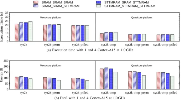
In full SRAM cache hierarchy, which is the baseline scenario, we observe in Figures 4a and 4b that the optimized versions are better as expected than the non-optimized version, in terms of execution time and Energy-to-Solution (or EtoS, i.e., the energy consumed for producing the execution results). The loop tiling and permutation respectively reduce the execution time by 26 % and 23 % and the EtoS by 24 % and 21 %. The loop tiling performs slightly better than loop permutation. B. Hybrid cache hierarchies
When only the L2 cache is in STT-MRAM, we observe in Figure 4a an overhead of 15 % on execution time for syr2k program compared to the execution of the same program in full SRAM cache hierarchy. Similarly, the syr2k-perm and syr2k-ptiledoptimized versions also show a lightweight overhead of 2 % and 1 % respectively, compared to their counter-part full SRAM configuration. This is due to the higher latency of the write operations on the L2 cache in STT-MRAM. Regarding EtoS, syr2k in hybrid cache hierarchy consumes more than with the full SRAM configuration. Nevertheless, with the loop transformations, we see an energy reduction over the full SRAM configuration. This can be explained by less penalizing memory operations for STT-MRAM, i.e., less write transactions in L2 STT-MRAM cache, which result from the applied optimizations. This contributes to mitigate the EtoS by reducing overall execution time. On the other hand, when moving the L1-instruction to STT-MRAM technology in addition to the L2 cache, the syr2k, syr2k-perm and syr2k-ptiledprograms considerably improve the EtoS. C. Full-STT-MRAM cache hierarchy
When considering a full STT-MRAM cache hierarchy, Figure 4b shows the best EtoS, which is reduced by 31 % on average. However, there is an important increase of 22 % in the execution time of syr2k program. Again, this is due to the high write operation latency on L1-data and L2 caches. Yet, in Figure 4a, we observe that this drawback of NVM is eliminated in the optimized programs. This means that the application of efficient optimizations on an NVM-based cache enables to better benefit from NVMs.
In a more detailed view, Figure 6a presents the energy breakdown of the entire system-on-chip, where the energy consumption of the main components of the considered architecture is reported, according to the distinguished cache hierarchy configurations. The results concern the execution of the syr2k-ptiled program. Thereby, we see how the integration of STT-MRAM at different cache levels improves the energy consumption for all represented components. Fo-cusing on L1-instruction, L1-data and L2, we clearly see that their static energy significantly decreases with STT-MRAM integration. Since the emphasis of NVMs is their extremely low-leakage power, the observed improvement of the EtoS
Quadcore platform Monocore platform
SRAM_SRAM_SRAM
SRAM_SRAM_STTMRAM STTMRAM_SRAM_STTMRAMSTTMRAM_STTMRAM_STTMRAM
E xe cu ti o n T im e (s ) 0 5 10 15 20 25 30 35
syr2k syr2k-perm syr2k-ptiled syr2k-omp syr2k-omp-perm syr2k-omp-ptiled
(a) Execution time with 1 and 4 Cortex-A15 at 1.0 GHz
Quadcore platform Monocore platform E n er gy ( J) 0 50 100 150 200 250
syr2k syr2k-perm syr2k-ptiled syr2k-omp syr2k-omp-perm syr2k-omp-ptiled
(b) EtoS with 1 and 4 Cortex-A15 at 1.0 GHz
Fig. 4. Summary of global execution time and EtoS on monocore and multicore platforms
comes from this property of NVM which drastically improves the static energy of memories.
VI. ENERGY AND PERFORMANCE ANALYSIS OF MULTICORE APPLICATION CODE OPTIMIZATION
In this section, we explore the effect of the parallelization on a multicore platform with similar cache memory configurations as discussed in Section V. We start with a full SRAM cache hierarchy and we progressively integrate STT-MRAM at different cache levels in order to assess their impact on performance and EtoS.
The considered platform is composed of four ARM Cortex-A15 cores operating at 1.0 GHz. The executed programs are depicted by Figures 2b and 2d. We use the same optimizations as presented in section V, and we add OpenMP pragmas. A. Full SRAM cache hierarchy
This configuration is our baseline and all subsequent com-parisons are made based on it. We evaluate its corresponding execution time and EtoS, which are respectively 9.46 seconds and 179 J.
Figure 4a shows that on a multicore platform with full SRAM cache hierarchy, the effect of the code parallelization is immediate. The execution is faster than the monocore execution, with a gain of 55 % in execution time. We do not get an even better speedup with four cores because the compiler, when parallelizing, outlines the loop to a dedicated function in order to use pthreads. By doing that, it loses track of pointer analysis and ends up generating worse code for the loop body, mitigating the speedup brought by parallelism. On the other hand, the EtoS increases by 66 %, from 107 J to 179 J. The reason of this increase is the addition of more components (a large part is multiplied by four) on the chip, which makes higher the overall dissipated leakage power.
B. Hybrid cache hierarchy
When integrating STT-MRAM in the cache hierarchy, an overhead is observed in execution time and EtoS, as depicted in figure 4a and 4b. Regarding the execution time, this is explained by the higher write operation latency in the L2 cache. Here, with a L2 cache in STT-MRAM, this overhead is around 13 %. When integrating STT-MRAM in both L1-instruction and L2 caches, the execution time remains the same. This indicates that using a read-only L1-instruction cache in STT-MRAM does not introduce additional penalty on execution time, but the energy consumption decreases on average by 5 % thanks to the improved leakage power of STT-MRAM.
C. Full-STT-MRAM cache hierarchy
With a full STT-MRAM cache hierarchy, the execution time becomes longer (8 % on average) compared to the full SRAM scenario, but the energy consumption is decreased by 20 % on average. As shown in Figure 5, the programs that take into account code optimizations show better results in terms performance/energy trade-off. Without code optimizations, execution time is increase by 17.1 % while the EtoS is decrease by 15.2 %. When applying code optimizations, the execution time penalty becomes 5.4 % and 3.4 % while the EtoS gains are 22.9 % and 24.2 %, for syr2k-omp-perm and syr2k-omp-ptiled respectively. This suggests that applying adequate code optimizations can result in very promising energy-efficient executions on multicore platforms.
VII. GAINED INSIGHTS
An important observation from the study exposed in this paper is that the operating frequency of systems has a significant impact on the performance of NVMs as illustrated in Figure 3. The identified frequency ranges could typically be used by a system kernel to tune available operating frequencies according to a dynamic voltage frequency scaling mechanism. This could
SRAM_SRAM_SRAM
SRAM_SRAM_STTMRAM STTMRAM_SRAM_STTMRAMSTTMRAM_STTMRAM_STTMRAM
E n er gy ( J) 0,01 0,1 1 10 100
Core Bus Mem. Ctrl L1i dyn L1i static L1d dyn L1d static L2 dyn L2 static
(a) syr2k-ptiled program executed on monocore platform with different memory scenarios
E n er gy ( J) 0,01 0,1 1 10 100
Core Bus Mem. Ctrl L1i dyn L1i static L1d dyn L1d static L2 dyn L2 static
(b) syr2k-omp-ptiled program executed on multicore platform with different memory scenarios Fig. 6. Examples of energy breakdown on monocore and multicore platforms
ref-SRAM_SRAM_SRAM ref-SRAM_SRAM_STTMRAM ref-STTMRAM_SRAM_STTMRAM ref-STTMRAM_STTMRAM_STTMRAM perm-SRAM_SRAM_SRAM perm-SRAM_SRAM_STTMRAM perm-STTMRAM_SRAM_STMMRAM perm-STTMRAM_STTMRAM_STTMRAM ptiled-SRAM_SRAM_SRAM ptiled-SRAM_SRAM_STTMRAM ptiled-STTMRAM_SRAM_STTMRAM ptiled-STTMRAM_STTMRAM_STTMRAM E n er gy ( J) 110 120 130 140 150 160 170 180 190 Execution Time (s) 7 8 9 10 11 12
Fig. 5. Performance/energy trade-off with 4 Cortex-A15 cores operating at 1.0 GHz. The reference case, denoted as ref-* is the syr2k-omp program. The other programs are optimized version of syr2k-omp
serve to ensure only optimal frequencies, i.e., enabling fast STT-MRAM memory operations compared to SRAM, so as to maintain good performance levels while decreasing the power consumption.
Taking a deeper look at the EtoS, we can draw further interesting conclusions. Figures 6a and 6b depict the EtoS of each part of the architecture. As expected, the main benefits in percentage arise from the memory blocks. Both static and dynamic energy consumed in caches are reduced or significantly reduced for some specific configurations such as the full
STT-MRAM cache hierarchy. For this specific case, the static energy consumption of the cache is decreased by more than 90 % while the dynamic energy consumption is reduced by more than 60 %. The other parts of the design such as core or bus only suffer of a small increase (about 3 %) of their energy consumption. This is directly related to the increase in the execution time. At the end, the benefit of the STT-MRAM is much larger (i.e., 39 J) than the penalty in energy (3 J) due to the execution time growth.
Concerning compiler optimizations, it has been known for a long time that finding the optimal set of optimizations for a piece of code (including their order, and their parameters – such as the tile size) is a daunting task. This study shows that it is even more true in the presence of NVM: first, the type of memory adds a new dimension to the search space; second, current compilers have been tuned to optimize for SRAM, not NVM. The produced code is hence sub-optimal in the presence of NVM.
VIII. CONCLUSION AND PERSPECTIVES
In this paper, we presented an empirical impact analysis about energy-efficiency when executing typical compiler-optimized codes on embedded multicore architectures inte-grating STT-MRAM memory technology. We considered two loop nest optimizations (tiling and permutation) on single-core and quad-single-core ARM Cortex-A15 platforms to show performance improvements. At the same time, the significant reduction in leakage power enabled by STT-MRAM compared to SRAM, decreases the overall energy consumption on both execution platform case studies (up to 31 % and 24.2 % as shown in Sections V and VI respectively). At the same time, the performance observed with SRAM has been reasonably preserved, e.g., only 3.4 % less on the studied multicore platform compared to a system with a full SRAM cache hierarchy (see Section VI). his has been achieved through a
detailed study on the most favorable core operating frequency. A key insight gathered in this study is that this gain in energy-efficiency depends on the correlation between NVM technologies and their operating frequencies.
Though this empirical study has been presented in this paper through a simple kernel, very similar observations were obtained when we extended the study to further workloads of the Polybench benchmark suite [25].
In our future work, we plan to design novel compiler optimizations tuned for NVM technologies. In the current work, we put the focus on the ARM Cortex-A15 core, which is a high-performance CPU. It will be worthy to extend this study to low power CPUs like the Cortex-A7 core. We believe that using such CPUs in multicore platforms with NVMs could result in very important energy-efficiency.
ACKNOWLEDGMENT
This work has been partially funded by the French ANR agency under the grant ANR-15-CE25-0007-01, within the framework of the CONTINUUM project.
REFERENCES
[1] K. Bergman, S. Borkar, D. Campbell, W. Carlson, W. Dally, M. Denneau, P. Franzon, W. Harrod, J. Hiller, S. Karp, S. Keckler, D. Klein, R. Lucas, M. Richards, A. Scarpelli, S. Scott, A. Snavely, T. Sterling, R. S. Williams, and K. Yelick, “Exascale computing study: Technology challenges in achieving exascale systems,” 2008.
[2] “The Mont-Blanc project – European Approach Towards Energy Efficiency,” Opto Speed SA. [Online]. Available: https://www. montblanc-project.eu
[3] S. Senni, L. Torres, G. Sassatelli, A. Gamati´e, and B. Mussard, “Exploring MRAM technologies for energy efficient systems-on-chip,” IEEE Journal on Emerging and Selected Topics in Circuits and Systems, vol. PP, no. 2, pp. 1–14, 2016.
[4] N. Binkert, B. Beckmann, G. Black, S. K. Reinhardt, A. Saidi, A. Basu, J. Hestness, D. R. Hower, T. Krishna, S. Sardashti, R. Sen, K. Sewell, M. Shoaib, N. Vaish, M. D. Hill, and D. A. Wood, “The gem5 simulator,” SIGARCH Comput. Archit. News, vol. 39, no. 2, pp. 1–7, Aug. 2011. [5] X. Dong, C. Xu, Y. Xie, and N. P. Jouppi, “Nvsim: A circuit-level
performance, energy, and area model for emerging nonvolatile memory,” Computer-Aided Design of Integrated Circuits and Systems, IEEE Transactions on, vol. 31, no. 7, pp. 994–1007, 2012.
[6] S. Li, J. H. Ahn, R. D. Strong, J. B. Brockman, D. M. Tullsen, and N. P. Jouppi, “McPAT: An integrated power, area, and timing modeling framework for multicore and manycore architectures,” in Proceedings of the 42nd Annual International Symposium on Microarchitecture, ser. MICRO 42. ACM, 2009, pp. 469–480.
[7] A. V. Khvalkovskiy, D. Apalkov, S. Watts, R. Chepulskii, R. S. Beach, A. Ong, X. Tang, A. Driskill-Smith, W. H. Butler, P. B. Visscher, D. Lottis, E. Chen, V. Nikitin, and M. Krounbi, “Basic principles of STT-MRAM cell operation in memory arrays,” Journal of Physics D: Applied Physics, vol. 46, no. 7, 2013.
[8] D. F. Bacon, S. L. Graham, and O. J. Sharp, “Compiler transformations for high-performance computing,” ACM Comput. Surv., vol. 26, no. 4, pp. 345–420, Dec. 1994. [Online]. Available: http://doi.acm.org/10.1145/197405.197406
[9] Q. Li, J. Li, L. Shi, C. J. Xue, and Y. He, “MAC: migration-aware compilation for STT-RAM based hybrid cache in embedded systems,” in Proceedings of the 2012 international symposium on Low power electronics and design, 2012, pp. 351–356.
[10] Q. Li, M. Zhao, C. J. Xue, and Y. He, “Compiler-assisted preferred caching for embedded systems with STT-RAM based hybrid cache,” ACM SIGPLAN Notices, vol. 47, no. 5, pp. 109–118, 2012.
[11] M. R. Guthaus, J. S. Ringenberg, D. Ernst, T. M. Austin, T. Mudge, and R. B. Brown, “MiBench: A free, commercially representative embedded benchmark suite,” in Workload Characterization, WWC-4. IEEE International Workshop on, 2001, pp. 3–14.
[12] Y. Li, Y. Chen, and A. K. Jones, “A software approach for combating asymmetries of non-volatile memories,” in Proceedings of the 2012 international symposium on Low power electronics and design. ACM, 2012, pp. 191–196.
[13] Y. Li, A. Abousamra, R. Melhem, and A. K. Jones, “Compiler-assisted data distribution for chip multiprocessors,” in Proceedings of the 19th international conference on Parallel architectures and compilation techniques. ACM, 2010, pp. 501–512.
[14] Synopsis Inc., “HSPICE manuals,” Mountain View, CA, 2003. [15] P. S. Magnusson, M. Christensson, J. Eskilson, D. Forsgren, G. Hallberg,
J. Hogberg, F. Larsson, A. Moestedt, and B. Werner, “Simics: A full system simulation platform,” Computer, vol. 35, no. 2, pp. 50–58, 2002. [16] A. W. Appel, Modern Compiler Implementation in C. Cambridge
University Press, 1998.
[17] Y. Huang, T. Liu, and C. J. Xue, “Register allocation for write activity minimization on non-volatile main memory for embedded systems.” Journal of Systems Architecture - Embedded Systems Design, vol. 58, no. 1, pp. 13–23, 2012.
[18] Q. Li, Y. He, J. Li, L. Shi, Y. Chen, and C. J. Xue, “Compiler-assisted refresh minimization for volatile stt-ram cache.” IEEE Trans. Computers, vol. 64, no. 8, pp. 2169–2181, 2015.
[19] J. Zambreno, M. T. Kandemir, and A. Choudhary, Embedded Software: Second International Conference, EMSOFT, 2002, ch. Enhancing Com-piler Techniques for Memory Energy Optimizations, pp. 364–381. [20] S. V. Gheorghita, H. Corporaal, and T. Basten, “Iterative compilation for
energy reduction.” J. Embedded Computing, vol. 1, no. 4, pp. 509–520, 2005.
[21] F. Bodin, T. Kisuki, P. M. W. Knijnenburg, M. F. P. O’Boyle, and E. Rohou, “Iterative compilation in a non-linear optimisation space,” in Workshop on Profile and Feedback-Directed Compilation (FDO-1), in conjunction with PACT, Oct. 1998.
[22] P. Marchal, J. I. G´omez, and F. Catthoor, “Optimizing the memory bandwidth with loop fusion,” in Proceedings of the 2nd International Conference on Hardware/Software Codesign and System Synthesis, ser. CODES+ISSS ’04, 2004, pp. 188–193.
[23] M. T. Kandemir, I. Kolcu, and I. Kadayif, “Influence of Loop Opti-mizations on Energy Consumption of Multi-bank Memory Systems,” in Proceedings of the 11th International Conference on Compiler Construction, ser. Lecture Notes in Computer Science, vol. 2304. Springer International Publishing, 2002, pp. 276–292.
[24] M. Kandemir, N. Vijaykrishnan, M. J. Irwin, and W. Ye, “Influence of compiler optimizations on system power,” IEEE Trans. Very Large Scale Integr. Syst., vol. 9, no. 6, pp. 801–804, Dec. 2001.
[25] “Polybench Benchmark,” Ohio State University. [Online]. Available: https://sourceforge.net/projects/polybench
[26] T. Kisuki, P. M. W. Knijnenburg, and M. F. P. O’Boyle, “Combined selection of tile sizes and unroll factors using iterative compilation.” in International Conference on Parallel Architectures and Compilation Techniques (PACT). IEEE Computer Society, 2000, pp. 237–248. [27] HardKernel, “Odroid XU4,” http://www.hardkernel.com.
[28] Samsung, “Exynos octa 5422,” 2015.
[29] C. W. Smullen, V. Mohan, A. Nigam, S. Gurumurthi, and M. R. Stan, “Relaxing non-volatility for fast and energy-efficient STT-RAM caches,” in High Performance Computer Architecture (HPCA), 17th International Symposium on. IEEE, 2011, pp. 50–61.
[30] A. Jog, A. K. Mishra, C. Xu, Y. Xie, V. Narayanan, R. Iyer, and C. R. Das, “Cache revive: architecting volatile STT-RAM caches for enhanced performance in CMPs,” in Proceedings of the 49th Annual Design Automation Conference. ACM, 2012, pp. 243–252.
[31] C. Layer, L. Becker, K. Jabeur, S. Claireux, B. Dieny, G. Prenat, G. D. Pendina, S. Gros, P. Paoli, V. Javerliac, F. Bernard-Granger, and L. Decloedt, “Reducing system power consumption using check-pointing on nonvolatile embedded magnetic random access memories,” ACM Journal on Emerging Technologies in Computing Systems (JETC), vol. 12, no. 4, p. 32, 2016.
[32] G. Prenat, K. Jabeur, P. Vanhauwaert, G. D. Pendina, F. Oboril, R. Bishnoi, M. Ebrahimi, N. Lamard, O. Boulle, K. Garello, J. Langer, B. Ocker, M. C. Cyrille, P. Gambardella, M. Tahoori, and G. Gaudin, “Ultra-fast and high-reliability sot-mram: From cache replacement to normally-off computing,” IEEE Transactions on Multi-Scale Computing Systems, vol. 2, no. 1, pp. 49–60, Jan 2016.
[33] T. Lanier, “Exploring the design of the Cortex-A15 processor,” URL: http://www. arm. com/files/pdf/atexploring the design of the cortex-a15. pdf (visited on 18/05/2016), 2011.