Characterization and Mitigation of Process
Variation in Digital Circuits and Systems
by
Nigel Anthony Drego
B.S., Computer Engineering, University of California, Irvine (2001)
S.M., Electrical Engineering & Computer Science, Massachusetts
Institute of Technology (2003)
Submitted to the Department of Electrical Engineering and Computer
Science
in partial fulfillment of the requirements for the degree of
Doctor of Philosophy
at the
MASSACHUSETTS INSTITUTE OF TECHNOLOGY
June 2009
MASSACHUSETTS INSTITUTE
OF TECHNOLOGY
AUG 0
7
2009
LIBRARIES
@
Massachusetts Institute of Technology 2009. All rights reserved.
ARCHIVES
Author
...
...
-,
...
Department of Electrical Engineering and Computer Science
Certified by.
Professor of Electrical Engineering &
4pril 24, 2009
DuaneBoning
Computer Science
,Thesis Supervisor
Certified by.
Accepted by.
Anantha Chandrakasan
Professor of Electrical Engineering & Computer Science
Thesis Supervisor
/
Terry P. Orlando
Characterization and Mitigation of Process Variation in
Digital Circuits and Systems
by
Nigel Anthony Drego
Submitted to the Department of Electrical Engineering and Computer Science on April 24, 2009, in partial fulfillment of the
requirements for the degree of Doctor of Philosophy
Abstract
Process variation threatens to negate a whole generation of scaling in advanced pro-cess technologies due to performance and power spreads of greater than 30-50%. Mitigating this impact requires a thorough understanding of the variation sources, magnitudes and spatial components at the device, circuit and architectural levels. This thesis explores the impacts of variation at each of these levels and evaluates techniques to alleviate them in the context of digital circuits and systems.
At the device level, we propose isolation and measurement of variation in the intrinsic threshold voltage of a MOSFET using sub-threshold leakage currents. Anal-ysis of the measured data, from a test-chip implemented on a 0. 18pm CMOS process, indicates that variation in MOSFET threshold voltage is a truly random process de-pendent only on device dimensions. Further decomposition of the observed variation reveals no systematic within-die variation components nor any spatial correlation.
A second test-chip capable of characterizing spatial variation in digital circuits is developed and implemented in a 90nm triple-well CMOS process. Measured variation results show that the within-die component of variation is small at high voltages but is an increasing fraction of the total variation as power-supply voltage decreases. Once again, the data shows no evidence of within-die spatial correlation and only weak systematic components. Evaluation of adaptive body-biasing and voltage scaling as variation mitigation techniques proves voltage scaling is more effective in performance modification with reduced impact to idle power compared to body-biasing.
Finally, the addition of power-supply voltages in a massively parallel multicore processor is explored to reduce the energy required to cope with process variation. An analytic optimization framework is developed and analyzed; using a custom sim-ulation methodology, total energy of a hypothetical 1K-core processor based on the RAW core is reduced by 6-16% with the addition of only a single voltage. Analysis of yield versus required energy demonstrates that a combination of disabling poor-performing cores and additional power-supply voltages results in an optimal trade-off between performance and energy.
Thesis Supervisor: Duane Boning
Title: Professor of Electrical Engineering & Computer Science
Thesis Supervisor: Anantha Chandrakasan
Acknowledgments
Though a PhD is primarily the undertaking of a single person, it cannot be done without the aid of many others. I have been infinitely blessed to be surrounded by family, friends, labmates, colleagues and professors who have provided support and aid throughout this PhD.
I would first like to thank my research advisors, Prof. Duane Boning and Prof. Anantha Chandrakasan who have provided not only technical and research guidance, but practical advice on many other topics as well. I couldn't ask for better advisors over the course of the past four years - I have learned a lot from both of you and I only hope that throughout my career, I am able to pass along a fraction of the wisdom and learnings you have passed on to me.
Two other professors provided excellent support and guidance over the last year of my PhD. The third member of my thesis committee, Prof. Anant Agarwal, pointed us in the right direction when it came to understanding the future of multicore pro-cessors and the critical research needs to enable continued performance scaling. Prof. Devavrat Shah's masterful command of mathematics and optimization thoroughly aided me during the last part of my PhD. I am grateful for Prof. Shah's time and patience in helping me to understand optimization and mathematical bounding of the optimization problem I faced.
My family has been a continuing source of love and support throughout my life, no less so during my PhD. To Mom, Dad, Roulla, Priya, Pathy and Naveen, I know how proud you are of me and the culmination of this work and I can't thank you enough for the unconditional backing you have always provided and continue to provide. To Vid, arguably you deserve this PhD even more than I do - it has been you that has been my source of sanity. You are my rock of support both in times of difficulty and otherwise, and a counterpoint, providing a cool head in times of frustration and a "kick in the rear" when I've lacked motivation. Without you, it's impossible to imagine this ever being undertaken or completed - Thank You!
four years, I have been extremely fortunate to meet and be in the company of a stellar group of friends. Anand and Nammi, you are our extended family here. You took us in when we were searching for housing out here and since then you've provided both Vid and myself with so many laughs, good times, diversions and some amazing chocolate chip cookies! Naveen and Yogesh, you both are exceptional friends who have helped me so much, both technically and otherwise. Coffee hour has been such a critical part of my PhD and I do not look forward to the day that ends. There are many other friends who must be acknowledged for their many contributions to my technical understanding and/or well-being over the past four years, including Karthik Balakrishnan, Daihyun Lim, Karen and Andy Gettings and Anita Misri as well as Nicholas Velastegui and Steve Pfeiffer from my days at Intel. In addition, I can't thank Debb Hodges-Pabon enough for being another mother and such a wonderful confidant and human-being. Debb, you truly do make everyone's MTL experience so much better.
I am grateful to all the past and present members of both the Boning and Anantha research groups, with whom I've shared many an interesting conversation and who have helped me in many capacities.
The authors acknowledge the support of the Focus Center for Circuit & System Solutions (C2S2), one of five research centers funded under the Focus Center Research Program, a Semiconductor Research Corporation Program.
Contents
1 Introduction 17
1.1 Thesis Organization ... 20
1.2 Thesis Contributions ... ... ... 21
2 Process Variation In Context 23 2.1 Sources of Variation ... ... 23
2.1.1 Lithography ... ... .. .. .. . .. .. . ... . .. . . .. 25
2.1.2 Plasm a Etch ... 26
2.1.3 Ion Implantation & Annealing . ... . . . . . 27
2.1.4 Chemical-Mechanical Polishing (CMP) ... 28
2.1.5 Other Variation Sources ... 29
2.2 Impact on Transistor Parameters ... 30
2.2.1 Mobility (p) ... . ... 31
2.2.2 Oxide Capacitance (C"o) ... . ... 33
2.2.3 Transistor Dimensions (W, L) . ... 33
2.2.4 Threshold Voltage (VT) ... 35
2.2.5 Device Impact Summary ... 36
2.3 Decomposing Variation ... 37
2.4 Impact to Modeling and Design of Circuits and Systems ... . 41
2.5 Background & Related Work ... 43
2.5.1 Characterization ... 44
2.5.2 Mitigation ... . ... .. 49
2.5.3 Modeling & Simulation . ... ... 53
3 Device Parameter Variation: Threshold Voltage
3.1 Motivation ... ... ... 55
3.2 Theory & Enabling Circuits ... .... 57
3.2.1 Extraction of AVTo ... . .. ... 57
3.2.2 Test-Structure Architecture & Circuits . ... . .. . . . 60
3.2.3 Simulation Results of AVT Isolation .. . ... .. . . .. 63
3.3 Data Analysis ... . ... ... .. 66
3.3.1 ADC Performance . . . . . .. . . . .. . . 66
3.3.2 Current Measurements and Extracted VT ... . . . .. . . 68
3.3.3 Pelgrom Modeling ... ... . 69
3.3.4 Intra-Die Spatial Correlation . ... 70
3.3.5 Die-to-Die Correlation ... . . . . . . . . . . 72
3.4 Design and Modeling Implications ... . .. . .. . . . . . 74
3.4.1 Circuit Modeling . . . . . .... ... ... 74
3.4.2 Circuit Design ... ... . ... . . 76
3.5 Summary .. . . ... ... ... . . 78
4 Digital Circuit Performance Variation 79 4.1 Motivation . . . . . .. . ... . . . . . .. . . 80
4.2 Test Circuits & Chip Architecture ... .... . . . . . 81
4.2.1 High Frequency Test Circuits ... . . . . .. 81
4.2.2 High-Resolution Digital Delay Measurement . . . . 84
4.2.3 Body-Biasing Circuits ... . . . . ... . ... 89
4.3 Data Analysis ... .. . ... ... .. 90
4.3.1 Variation Measurements . ... ... ... . . 90
4.3.2 Spatial Variation & Correlation ... . . . 91
4.3.3 Adder Bit Delays ... . ... ... .96
4.4 Variation Mitigation ... .. ... .. .. .. . 101
4.4.1 Dependence on Performance Domain .. ... ... . 102
4.4.2 Adaptive Body-Biasing . . ... .... .... . ... 102
8
4.4.3 Adaptive Power-Supply Voltage Scaling . . . . . .. . . . 104
4.5 Summary .. ... ... 107
5 Variation Mitigation at the Architectural Level 109 5.1 Impact of Variation on Multi-Core Processors ... . . . . . 110
5.2 Mitigation Strategy: Multiple Power-Supply Voltages . ... . . 113
5.2.1 Problem Formulation ... 113
5.2.2 Energy Minimization . ... .. .. .. . . . .. . . . . 117
5.3 Mitigation Results ... ... . 120
5.3.1 Analytic Energy Reduction . . . . 121
5.3.2 Simulation Methodology ... .. 122
5.3.3 Results & Analysis ... ... .. 125
5.3.4 Practical Considerations ... 130
5.4 Sum m ary ... ... ... .. 140
6 Thesis Summary & Future Work 143 6.1 Thesis Summary ... 143
6.2 Future W ork ... 145
6.2.1 D evices . . . 145
6.2.2 Circuits . . . 146
6.2.3 Architectures & Systems ... ... 148
A Performance of MEVS Algorithm 151 A.1 Proof of Optimality for N = 2 ... . 151
List of Figures
1-1 Two "nominally" identical transistors that are physically different due
to a variety of causes ... 18
1-2 Frequency and leakage variations of Intel microprocessors on a single w afer [1] . . . . . . . .. .. 19
2-1 Cross-section of a MOSFET ... 23
2-2 Cross-sectional view of a CMOS integrated circuit with major steps needed for fabrication [2]. . .... . ... ... . 24
2-3 Line-edge Roughness (LER) [3] ... 26
2-4 Intel simulation of Random Dopant Fluctuation (RDF) [4]. ... . 28
2-5 Dishing of copper and erosion of inter-layer dielectrics in CMP... 29
2-6 Mobility as function of doping in Si [5]. . ... 32
2-7 ITRS projections for channel length variation [6, 7, 8, 9]. ... . 34
2-8 uVT has increased with continued technology scaling [10] ... 36
2-9 Decomposition of process variation into different length scales. .... 38
2-10 Decomposition of within-die spatial variation . ... 41
2-11 IBM's efforts in spatial variation characterization. . ... . . 46
2-12 Improvement in aVT in Intel's process due to oxide scaling and new ma-terials, though there is no mention of how 'vT scales. C2 is analogous IVT to AvT found in Eq. 2.7. Reproduced from [11]. . ... . 50
2-13 RazorII latch capable of detecting timing errors and restarting the pipeline [12] ... ... ... .. 52
3-2 Simplified VT variation architecture and circuits . ... . . . .... 60
3-3 Simplified schematic of individual bank .. . . .. . . . . . . . 61
3-4 Test-chip die photo. The DUT array is shown at left, with the ADC and digital control and calibtration blocks at right . . . . . . . . 62
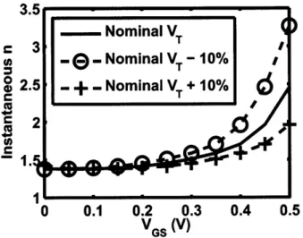
3-5 Current sensitivity to variation in VT, L . . . . . . . . ..... 64
3-6 INL plot for a single ADC . ... ... .. ... . . . 67
3-7 Spatial distributions of n and VT for a single die . . ... .. . . 69
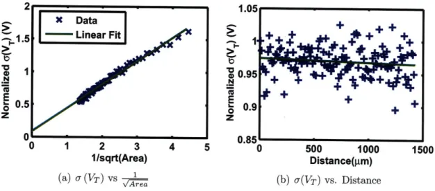
3-8 Pelgrom fits of a (VT) ... ... 70
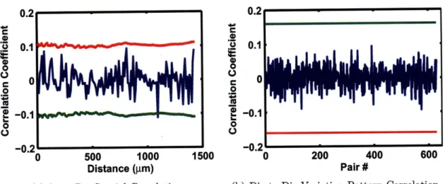
3-9 Intra-die correlation vs. distance and die-to-die pattern correlation .. 71
3-10 VT distribution and normal probability plot for a single die ... . . 72
3-11 Decomposition of within-die spatial variation, including VT variation. 73 3-12 Circuit performance correlation as a function of VDD . . . . . . . 75
4-1 Arrayed Kogge-Stone adders instrumented for internal delay measure-ment... . . . . .... . 81
4-2 Oscillating 64-bit Kogge-Stone adder . . . ... 82
4-3 32-bit asynchronous frequency counter comprised of toggle flip-flops.. 84
4-4 Graphical depiction of random sampling . ... 86
4-5 PFD and associated timing diagram . . . . ... ... . . 88
4-6 Random clock generation using a LFSR and variable drive-strength ring-oscillator ... . ... ... ... 88
4-7 Distribution of clock periods of random sampling clock . . . . 89
4-8 Variation as a function of VDD . . . . . .. ... ... ... 91
4-9 Adder spatial correlation as a function of VDD . . . ... ... 92
4-10 Systematic within-die variation ... . ... . . . 93
4-11 Adder spatial correlation as a function of VDD with systematic compo-nents removed ... .. ... 94
4-12 Decomposition of within-die spatial variation, including digital circuit performance variation. ... . .. . . . . ... ... . . 95
4-13 Inverter spatial correlation plots showing different decreases in die-to-die correlation with decreasing voltage based on number of stages. .. 95 4-14 Scatter matrices of each pair-wise combination of circuit types showing
no cross-circuit correlation at VDD = 1V. All circuit pairings are within the same "adder-block." ... 97 4-15 Bit delay measurements relative to Sum(0) . ... . . .98 4-16 Within-adder bit-slice cross-correlations revealing the logarithmic
struc-ture of the adder . ... ... ... . ... .. .. .. . ... . .. ... 99 4-17 Correlation between bit-slice delays and frequencies of the adder they
are a part of. Anti-correlation is due to comparing delays versus fre-quencies - an inverse relationship ... . . . 100 4-18 Spatial correlation between bit-slices 19 and 49 (blue dots) and
associ-ated confidence intervals (triangles). Strong correlation is only noticed for bit-slices within the same adder. . ... . 101 4-19 KS adder frequency deviation from nominal (no body-bias) versus
body-bias magnitude ... ... ... .. 104
4-20 Simulations of adder leakage current deviation from nominal (no body-bias) versus body-bias magnitude . ... . . . . 104
4-21 Adder performance as a function of power-supply voltage, VDD .... 105
4-22 Relative change in leakage as a function of relative change in frequency when body-biasing or VDD scaling are used for variation mitigation. . 106
5-1 Block diagram of a CMP with each core able to select from N volt-ages and example core voltvolt-ages, with normalized energies, to meet a
performance constraint ... ... 112
5-2 Example Vmin distribution and discretization for 1K-core RAW
proces-sor based CM P ... ... 116
5-3 Single optimum for both N = 2 and N > 2 . ... 118 5-4 Actual algorithm performance (stars = simulation data points, dashed
5-5 Analytic computation of Eoverhead and reduction of Eoverhead when using additional voltages selected by the MEVS algorithm. . ... 122 5-6 Simulation methodology to efficiently evaluate MEVS algorithm and
resultant energy savings . . . ... ... 123 5-7 1K-point Monte-Carlo voltage sweeps for a single critical path . . . . 125 5-8 Vector distance and energy difference between MEVS-selected and
globally optimal vectors. ... ... 126
5-9 Energy reduction ... ... 127
5-10 Joint performance/energy metric versus yield ... 129 5-11 Analytic computation of Eoverhead and reduction of Eoverhead versus core
yield constraint ... .... .. ... . 130
5-12 Variation in core leakage currents reduces to << 1% with even
mod-erate core size. ... .. ... ... 131
5-13 Leakage current as a function of VDD and temperature (normalized to
VDD - 1.V and T = 250C) ... 133
5-14 Core voltage assignment patterns. Dark squares indicate core is using V2 while white squares indicate V. . ... . 136 5-15 Pattern of cores changing between V and V2 as voltage/frequency
set-tings are changed ... . . . .. . ... 137
5-16 Energy using multiple system voltages relative to ideal energy when voltage regulator efficiencies are taken into account. . ... 139
List of Tables
2.1 Process modules affecting various transistor parameters. . ... 31 2.2 Variability in delay and power based on circuit-style [13]. ... . 37 2.3 Contributions of variation from individual parameters over various
cir-cuits and circuit styles, summarized from data in [13]. . ... 37 2.4 Characterization methodologies for each level of the design hierarchy. 45 2.5 Mitigation strategies for each level of the design hierarchy. ... 49
3.1 Extracted VT variation vs. subjected variation . ... 65 3.2 Simulated current differences due to inclusion and variation within
access transistors (IVGsl = 0.35V and |VDs| = 0.3V). . ... 66
5.1 Energy penalty of adjusting V to match nominal core-voltage
Chapter 1
Introduction
The continued integration and compression of the modern electronics we often take for granted has been the result of continuous transistor scaling. A device like the iPhone, that combines communication, entertainment, navigation and personal infor-mation management, is simply impossible to construct in its given form factor without integrating hundreds of millions, if not billions, of transistors, each with dimensions of 90nm or smaller. Modern microprocessors are comprised of transistors with elec-trical properties that can be described by numbers of atoms present or thicknesses counted by the number of atomic layers stacked. Perhaps more astonishing is that this steadfast increase in transistor density, known as Moore's Law [14], has provided faster and more powerful electronics with constant or even decreasing cost.
In 1965, Gordon Moore observed that the density of transistors on a die increased by a factor of two every 18 months -an observation that was quickly dubbed "Moore's Law" [14]. The decreased cost and increased performance associated with increased density makes an electronics consumer believe that a particular device purchased today will either be cheaper or have more features for the same cost in the future (i.e., the consumer implicitly takes Moore's Law to be a law rather than an observa-tion). Upon closer inspection however, there have been and continue to be many a technological hurdle to overcome in advancing Moore's observation. One of the most worrisome challenges in the current decananometer era of semiconductors is varia-tion: two nominally identical transistors, when fabricated, will vary in many respects
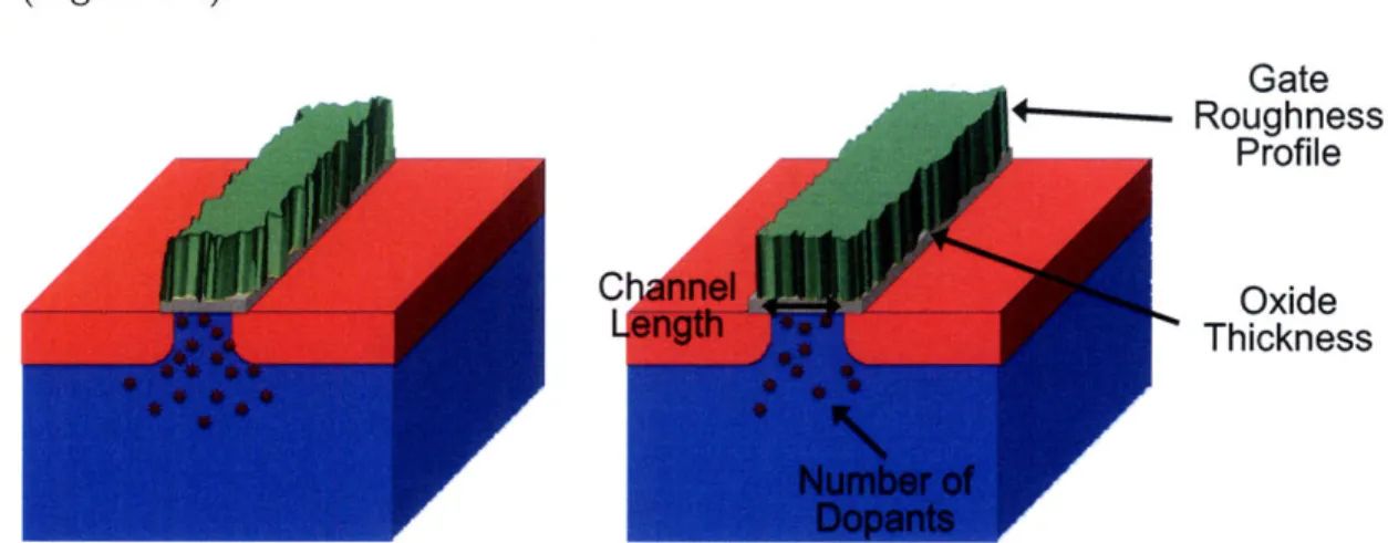
(Figure 1-1). Gate --- Roughness Profile
C
Oxide ThicknessFigure 1-1: Two "nominally" identical transistors that are physically different due to
a variety of causes.
This process variation is not new to manufacturing lines: typically known as process tolerance1, it is an established concept in a wide range of manufacturing processes, from biological to mechanical and agricultural to electrical, and including semiconductor manufacturing. However, in most cases the magnitude of the varia-tion is small relative to the nominal design parameters - with appropriate process control, these variations do not significantly impact the design nor the operation of the manufactured product. Until recently, this was the case in semiconductors as well: product-impacting variations were primarily due to and dominated by yield-loss defects and were mitigated or eliminated predominately with improved process control. Lately, however, this situation has deteriorated rapidly due to increasingly limited controllability of individual process modules operating at the limits, and in some cases beyond the originally intended limits.
To illustrate the impact of variation on actual products, Figure 1-2 plots the nor-malized distributions of frequency and standby leakage of Intel microprocessors on a single wafer. Parameter variations result in greater than 30% frequency spread and 20X variation in chip leakage. The large frequency spread necessitates expensive fre-quency binning in which each chip is tested to determine its maximum frefre-quency and power before it can be sold - an often expensive, time-consuming process. Moreover,
IProcess tolerance is the allowable variation in the parameters of a manufactured item that does not adversely affect the stated performance of that item.
as the standby leakage component of power increases as a fraction of the total power, 20X variation in leakage currents can mean that even if leakage is nominally only 1% of the total power, with variation it can be as much as 20%. In reality, variation in leakage power can result in variation of total power by as much as 50% [15].
1.4. Cr 151 Q 0 ZL01I (U
ff
.2 .1 .0-n O 0P
400
Oo
Bo
Oc
0 ~0o 0 0 020X
I I I I I I I I i S I I I I I I I I5
Normalize Leakage (isb)
Figure 1-2: Frequency and wafer [1]
leakage variations of Intel microprocessors on a single
As a result, yield is affected by parameter variations: chips that operate too slowly with high standby leakage power, or those that have high performance but are above the power envelope, must be discarded. Though microprocessors often represent extreme examples of semiconductor engineering, the problem is more generally valid: performance and power are significantly impacted by unmitigated parameter variation resulting in parametric yield loss. This poses a challenge that requires careful analysis and a paradigm shift as device engineers, circuit designers and system architects all must now consider process variation during the course of technology and product design and development.
0 0 V .~p~ I I I n
1.1
Thesis Organization
Effective mitigation of process variation requires both understanding and characteri-zation of its effects at all levels of design. As will be seen in Section 2.5, considerable work has been carried out in many areas of the variation spectrum. Work in one im-portant area, the characterization of spatial variation and its implications on digital circuits and systems, has been trailing, with only piecemeal contributions in very spe-cific contexts. This thesis provides a comprehensive, bottom-up analysis of within-die spatial process variation in the context of digital circuits and systems.
We begin in Chapter 2 by putting variation in context. A summary of variation sources in key process steps provides the basis for evaluating the impact of variation on individual transistor parameters. To better characterize and model variation, we explain how to decompose variation, particularly at the within-die level, drawing a distinction between systematic and spatially (un)correlated components. This allows evaluation of the impact this decomposition has to the modeling and design of digital circuits and systems. Background and related work are also provided to conclude the chapter.
Characterization and analysis of variation at the device level is undertaken in Chapter 3, by specifically focusing on the intrinsic threshold voltage, VTo, of a tran-sistor. Circuit designers are most often concerned about variation in channel length and VT. With comprehensive spatial analysis of channel length variation provided by Friedberg et al. in [16], similar analysis of VT variation became crucial. A test-chip capable of characterizing spatial variation of VTo by measuring the sub-threshold cur-rents of thousands of transistors is implemented and measured. Analysis of the data is performed to characterize both within-die spatial variation as well as any systematic spatial patterns repeatable from die-to-die. In combination with knowledge of spatial variation in channel length, Monte Carlo simulations are performed to understand the implications at the circuit level.
Chapter 4 focuses on abstracting away device parameter variation and under-standing spatial variation of common digital circuits. Here we detail a test-chip
architecture consisting of replicated blocks of digital circuits and high-precision mea-surement circuitry, implemented in a 90nm CMOS technology, that facilitates such understanding. The measured data from the test-chips are analyzed and compared to the Monte Carlo simulation results in Chapter 3. The results of Adaptive Body Biasing (ABB) as a potential mitigation scheme are also discussed and show that in advanced technologies Adaptive Voltage Scaling (AVS) is more effective.
Using the results and insights from the test-chips in Chapters 3 and 4, mitigation techniques at the architecture level are explored in Chapter 5. Specifically, we focus on future multi-core processors where the potential impact of within-die variation on both performance and power is significant. An analytic, mathematical approach is taken to choosing optimal power-supply voltage values in order to reduce energy. Using such an approach enables substantial energy savings, compared to a "worst-case" approach of using a single high-valued voltage, while meeting both yield and performance constraints, including core performance homogeneity, that are crucial to system designers and operating system architects.
Finally, Chapter 6 concludes with a high-level summary of this thesis, as well as suggestions for future research as informed by the findings outlined in the previous chapters.
1.2
Thesis Contributions
The major findings and contributions of this thesis are:
* Proposal of a measurement technique utilizing sub-threshold currents to effec-tively isolate and extract variation in the intrinsic threshold voltage of MOSFET transistors.
* Design and implementation of a test-chip using the proposed measurement tech-nique to characterize variation in an array of - 140K transistors.
* Design and implementation of an architecture to quantify spatial variation in digital circuits, including a high-speed, arbitrarily fine-resolution delay
mea-surement technique based on random-sampling and using only common digital components.
* Measurement analysis and decomposition of within-die variation for both MOS-FET threshold voltage and digital circuit performance into systematic (position-dependent), spatially correlated (distance-dependent) and spatially uncorre-lated components. In both cases, within-die variation is primarily random and spatially un-correlated (i.e., no spatially correlated component). In the case of digital circuit performance, a systematic component is identifiable but is small in magnitude relative to other components.
* Analysis (both through simulation and measured data) showing that variation sensing techniques included in mitigation schemes are highly dependent on the performance mode of a circuit, posing unique challenges for systems that scale between high-performance and low-power operating modes.
* Proposal, implementation and analysis of an analytic framework and algorithm for robust optimization and minimization of "variation-induced energy over-head" in massively parallel multi-core processors.
* A custom simulation methodology enabling the above framework and algorithm to be employed on a real core. These simulations demonstrated that a single ad-ditional power-supply voltage can reduce total energy consumption considerably in the face of variation.
Chapter 2
Process Variation In Context
Process variation is increasingly becoming a limiting factor in both IC design and manufacturing [17], as nearly every step in the IC manufacturing process introduces variation in the end device. This chapter explores the sources of semiconductor pro-cess variation, their impact, and related work in the field. We begin in Section 2.1 by enumerating the most significant of these variation sources, and discuss their impact on individual transistor parameters in Section 2.2. This is followed in Section 2.3 by a discussion of their spatial dependencies, and by analysis of impact to modeling and design of circuits and systems in Section 2.4. Finally, Section 2.5 summarizes previous research on variation in semiconductor manufacturing.
2.1
Sources of Variation
Surc Oxide ) Gate n
Lburce rain
O L P
SBody
Figure 2-1 depicts the lateral cross-section of a MOSFET in its most simple, ideal form and Figure 2-2 shows a cross-sectional view of an entire integrated circuit and the major steps involved in the fabrication of such a circuit. In Deep-Sub-Micron (DSM) CMOS, each of these requires one or more unit process steps. For example, formation of one of the two twin-well implants involves depositing or thermally growing an oxide layer, spinning on photoresist, lithographically patterning the photoresist to define the well area, developing away the exposed photoresist over the defined well areas, implanting the appropriate dopant species and then removing the resist and oxide layer. This entire procedure is then repeated for the other well. Variations of this procedure are used for each of the first thirteen steps listed in Figure 2-2. When forming the Shallow Trench Isolation (STI) and interconnect layers, additional polishing steps are required to ensure a smooth, uniform surface on which subsequent layers can be fabricated. Modern product designs require 100+ individual process steps to fully fabricate the entire CMOS stack.
1. Twin-well Implants
2. Shallow Trench Isolation Passivation layermetal
3. Gate Structure
4. Lightly Doped Drain Implants ILD-5
5. Sidewall Spacer ILD-4
6. Source/Drain Implants
7. Contact Formation
8. Local Interconnect ILD-2
9. Interlayer Dielectric to Via-i 10. First Metal Layer
11. Second ILD to Via-2
12. Second Metal Layer to Via-3 4 6
7 n-well p-well
13. Metal-3 to Pad Etch
p- Epitaxial layer
14. Parametric Testing
p+ Silicon substrate
Figure 2-2: Cross-sectional view of a CMOS integrated circuit with major steps needed for fabrication [2].
A number of these process steps can be highlighted as major sources of varia-tion [18]: 1) sub-wavelength lithography, 2) plasma etch, 3) ion implantavaria-tion and annealing, and 4) chemical-mechanical polishing (CMP). Depending on the feature being fabricated, each process step affects subsequent transistor and interconnect pa-rameters in differing manners: variations in lithography, etch and CMP affect the physical dimensions of transistors and the wires and vias that constitute the inter-connect between transistors. However, ion implantation and annealing directly affect the molecular make-up of transistors. Furthermore, the significance and impact of variation in a particular process step is highly dependent on not only the feature being fabricated, but also the application in which the fabricated transistor is used. For example, variation in the size of the source/drain area of a transistor may impact the overall performance far greater when that transistor is used in an analog versus digital application.
As critical dimensions continue to decrease, process variations become increasingly worrisome due to decreasing depth-of-focus of sub-wavelength lithography, line-edge roughness, random discrete dopant fluctuation, stress effects, and oxide thickness (to) fluctuation. In the following sub-sections, we identify some of the more significant sources of variation in each of the four process steps outlined above.
2.1.1
Lithography
Lithography is the process of exposing a light-sensitive material (photoresist, or just "resist") to define the critical physical dimensions of a semiconductor structure. Un-til the 180nm node, the wavelength of light used to pattern these critical dimen-sions scaled with the smallest of the dimendimen-sions to be patterned. In this regime lithography-induced variations were a result of lens imperfections, mask errors, illu-mination non-uniformity, and contributions arising from resist non-uniformities [19]. At the 180nm node, scaling of the wavelength of light used for patterning ceased at 193nm due to increased cost of lithography technology, materials, and equipment de-velopment and deployment. The resulting lithographic defocus causes both systematic and random line-width variations [20], mitigated to some degree by so-called
Resolu-tion Enhancement Techniques (RETs) such as Optimal Proximity CorrecResolu-tion (OPC), Sub-Resolution Assist Features (SRAF) and phase-shifted mask lithography [21].
Perhaps more alarming are random variations in line edges, known as Line-Edge Roughness (LER) and depicted in Figure 2-3, resulting in local variations in line-width [22]. The sources of this variation are still under discussion, but conjectures include shot noise of the energy of the light illuminating the resist, solubility and size of resist polymer particles, and local variations in the chemistries that make up chemically amplified resists [23].
(a) Nominal transis- (b) Transistor with (c) High-resolution (d) LER affecting
in-tor LER and RDF microscopy of LER terconnect
Figure 2-3: Line-edge Roughness (LER) [3]
Immersion lithography, extreme ultra-violet (EUV).lithography and improved re-sist materials may aid in improved control of physical gate and line dimensions. However, to date, only immersion lithography is commercially viable despite years of research related to EUV and improved resists.
2.1.2
Plasma Etch
After lithographic patterning, plasma etching is used to etch away unneeded areas of polysilicon, in the case of transistor gates, or an insulator, such as silicon dioxide or a low-k dielectric, in the case of interconnect. Variations in process conditions such as chamber temperature and pressure, RF power, electrode spacing, and gas flows often result in variations if not properly controlled using statistical process control [24]. Product layout, local chemistry non-uniformities and process conditions,
and lithography-induced variations also result in etch non-uniformities, giving rise to variation in side-wall profiles (varying slope of side-walls), line-widths, and thicknesses
(due to variation in etch depth). More detailed characterization and analysis of variations due to plasma etch can be found in the work of Abrokwah [25].
2.1.3
Ion Implantation & Annealing
Creation of transistors involves doping them with ions to define the type of transistor (PMOS or NMOS). The substrate, as well as other components of the transistor such as the highly-doped source/drain regions, are doped with different ion species (e.g. B, As, P). These ions are accelerated at high energy into the wafer during the ion implantation step and are then "activated" by heating the wafer (annealing) in order to ensure the implanted ions are properly substituted within the existing crystal structure of the underlying silicon substrate.
Once again, local and global process conditions such as implant energy and dose, tilt angle and temperature profiles all result in variations of the implanted ions. Lay-out features and proximity effects, such as distance to well edge, can also affect uniformity of ion implantation [18]. In the most advanced process technologies (e.g. 45/65nm technology nodes), device volumes are so small that only several tens to low hundreds of dopant atoms are needed within the channel area, directly underneath the gate, for the required doping concentrations. Due to the small numbers, variation in the dopant counts and even the placement of the atoms within the transistor body is of significant concern, as regions of a single transistor will experience different local doping concentrations. This variation mechanism is known as Random Dopant Fluc-tuation (RDF) and was brought to light as early as 1975 by Keyes [26]. The right of Figure 2-4 depicts RDF where the black dots in the channel are countable dopant atoms [4]. It is easy to see that by changing the number or even the placement of the atoms the electrical performance of the transistor can be greatly impacted. As transistor volumes continue to shrink, without individual placement of dopant atoms, RDF is unavoidable due to the decreasing absolute number of dopants required.
an-Figure 2-4: Intel simulation of Random Dopant Fluctuation (RDF) [4].
nealing become increasingly significant in modern processes, many have suggested moving to significantly different transistor structures, such as fully depleted devices (e.g., ultra-thin body or FinFET devices) [10]. However, acceptance of and transition to radically different device structures is both technologically and economically dif-ficult given the dominance and proven abilities of lateral MOSFETs. Consequently, the most common approach to mitigating this type of variation is to increase device size which reduces relative variation as the number of dopant atoms necessarily in-creases with device size. Such a solution is fundamentally incompatible with further transistor scaling, making it unsustainable in the long term and requiring solutions either at the process or design levels (i.e., improved process modules for the doping step, new device structures not requiring doping and/or circuit design that is robust to device variation).
2.1.4
Chemical-Mechanical Polishing (CMP)
CMP is used to achieve smooth and planar surfaces from which subsequent layers are able to be fabricated. Decreasing depth-of-focus in modern lithography systems underscores the need for exquisite planarity and without such planarity, features to be patterned may be out of focus due to surface height fluctuations (nanotopogra-phy) [27]. This results in subsequent lithographic variations as described in Sec-tion 2.1.1. However, CMP is not a variaSec-tion-free process itself: it is a significant
source of systematic variation resulting from both process conditions, including vari-ations in down force, rotational speed, pad conditioning, and temperature as well as designed feature sizes and pattern dependencies [28]. The primary effects of CMP variation are shown in Figure 2-5, where copper lines can be "dished" and inter-layer dielectrics eroded, causing variation in copper line thicknesses.
Dishing Erosion
Figure 2-5: Dishing of copper and erosion of inter-layer dielectrics in CMP.
Mitigation strategies for variation resulting from the CMP process module began with improved process control by using feedback from the process itself to guide when the polishing should end [29]. More recently, mitigation strategies have focused on improved modeling and design modification: since variations arising from the CMP process tend to be limited to pattern dependencies and features sizes, appropriate modeling of the process and product design can reveal areas of particular susceptibility to the types of variation depicted in Figure 2-5. With this information, automated mitigation strategies have been devised to enforce or adjust pattern densities (e.g., by using design rule constraints or automated "dummy fill" insertion) to dramatically reduce a design's susceptibility to CMP-caused variation [30].
2.1.5
Other Variation Sources
The four process modules described above contribute significantly to overall process variation, but variation is by no means limited to these four modules. Other process steps that are sources of variation include gate oxidation, polysilicon and nitride deposition, and metallization, all of which can result in variation in film thicknesses,
with varying degrees of impact to the fabricated transistor. Film thickness variation in polysilicon and interconnect metal are typically mitigated using CMP. However, as the previous section described, this can be a source of variation as well.
Variations in the gate oxidation step are primarily wafer-to-wafer due to differences in chamber temperature and length of time in the chamber. Within-wafer variations, due to temperature-induced stresses, lamp configuration and convective cooling, are corrected with better tool design as well as improved process control [31]. As a result, gate oxide and nitride layers are generally well controlled at the process module level but as dimensions continue to reduce, even small variations are amplified.
While we have described effective solutions for many of the variation sources described above, solutions for improved control of random discrete dopant fluctuation or oxide thickness at the manufacturing level do not exist, meaning these are issues circuit designers and system architects must increasingly be aware of and learn to deal with. Dealing with variation requires understanding how such fluctuations affect device properties, circuit performance and their architectural implications.
2.2
Impact on Transistor Parameters
Each of the variation sources highlighted above (and others) impacts the electrical properties of transistors and interconnect in unique and often subtle ways. These effects are best understood in the context of transistor performance. In a typical digital integrated circuit, a transistor either charges or discharges a capacitive load, and the time required to do so determines the performance of the transistor. This time is a function of the capacitance being driven, the voltage to which it must be driven and the current used to drive it, as shown in Eq. 2.1. For simplicity, we use the ideal I-V equation for a MOSFET in the saturation regime as shown in Eq. 2.2, where p is the mobility of a charge carrier through the device, Cox is the gate oxide capacitance, W and L are respectively the width and length of the transistor, VT is the device threshold voltage and VGS is the bias between gate and source. Though this equation is idealized and neglects important details in modern transistors, it is
sufficient to illustrate the impacts that the variation sources mentioned above have on a transistor. CloadVDD td = (2.1) 1 W ID uCoX (VGS - VT)' (2.2) 2 L CloadVDD td = Pc (VGS - VT)(2.3)
Table 2.1 shows the MOSFET parameters and relevant process modules that di-rectly affect each of those parameters. It is clear that a single process module can affect multiple transistor parameters, and thus decoupling the effects of one variation source from another are difficult. Nevertheless, we now explore variation from the perspective of the device, in particular each of the parameters listed in the table.
MOSFET Parameter Relevant Process Module(s)
p Ion implantation, annealing, diffusion, nitride deposition
Cox Gate oxidation
W, L Lithography, etch
VT Ion implantation, annealing, gate oxidation, (lithography, etch) Table 2.1: Process modules affecting various transistor parameters.
2.2.1
Mobility (
p)
Mobility refers to the ease which charge carriers (electrons or holes) can travel through the channel of a MOSFET in response to an applied electric field. It is mathematically defined as in Eq. 2.4, where q is the electronic charge, T is the mean free time between carrier collisions, and m,,p is the effective mass of either an electron (n) or hole (p). However, in practice, mobility is given as a function of the doping concentration as shown in Figure 2-6, since the doping concentration determines the mean free time between collisions, and to a lesser degree, the effective mass. In modern processes, stress engineering in the form of nitride liners and silicon germanium source/drains, also affects mobility by either stretching or compressing the silicon lattice to decrease
the effective mass of a particular charge carrier [32].
np - q (2.4)
n 2mn,p
Any process step which affects doping concentration or stress will necessarily affect transistor mobility. Therefore, ion implantation and annealing directly affect mobility as these process steps primarily determine doping concentrations. However, as seen in Figure 2-6, since doping concentration is on a log scale and typically does not vary by orders of magnitude from one transistor to another, the impact that ion implantation, annealing and other process modules that determine doping concentration have on mobility is relatively small.
1600 1400 1200 1000 800 600 400 200 'I
1E+14 1E+15 1E+16 1E+17 1E+18 1E+19 1E+20 1E+21
Doping (cm)
Figure 2-6: Mobility as function of doping in Si [5].
Intentional and unintentional stresses, whether by stress engineering or proximity to STI, can have large impacts on transistor mobility. Mobility improvements greater than 10% over unstrained silicon have been reported as strain engineering has ma-tured [33]. Even unintentional stresses due to STI proximity can cause within-die mobility variations on the order of a few percent depending on transistor distance to the STI edge [34]. Recent characterization of mobility in advanced processes indicates relatively large variation, 21% Z, and may be due to fluctuations in the intentional
stresses introduced in these processes [35].
electrons
holes n-Sin-Si
p-Si
p-Si n-Si
2.2.2
Oxide Capacitance (Cox)
Gate oxide capacitance is the capacitance between the gate stack (polysilicon and silicon dioxide) and the inverted channel of the MOSFET. Eq. 2.5 shows that the oxide capacitance is a function only of the oxide thickness (t,,) and the dielectric constant of silicon dioxide or other gate insulator.
Cox = (2.5)
tox
As mentioned in Section 2.1.5, gate oxidation (thermal growth of silicon dioxide or silicon nitride) is a relatively well controlled process step. However, with gate oxide thicknesses on the order of five atomic layers ( Inm), even small variations of one atomic layer have the potential to greatly impact not only oxide capacitance, but also threshold voltage and mobility [13]. With SiO2 gate oxide, variations of a
single monolayer (approximately 0.2nm) are typical and result in 20% shifts in oxide thickness. Furthermore, though not shown in Eq. 2.2, oxide thickness exponentially impacts gate currents due to Fowler-Nordheim tunneling [36]. As a result, variation in oxide thickness can have significant and pernicious effects on idle leakage power in modern devices. To improve this situation, Intel has recently begun using a "high-K" gate dielectric, hafnium dioxide (H
f02),
to allow for thicker gate oxides while maintaining oxide capacitance and gate control over the channel, but reducing gate leakage by three orders of magnitude [37, 38]. Moving to a new gate oxide material not only reduces gate leakage currents but reduces the impact of variability on Cox due to the much larger physical oxide thickness. Nevertheless, variations in the interfacial oxide of "high-K" stacks do still occur and can affect performance [39].2.2.3
Transistor Dimensions (W, L)
The previous section highlighted the importance of one of the smallest dimensions of a transistor, the gate oxide thickness. Eq. 2.2 shows that the width (W) and length
(L) of a transistor are critical in determining the current through that transistor.' W must be increased or L decreased to increase current and thus performance. Since decreasing L also reduces load capacitances and increases transistor density, scaling has continually reduced L in the pursuit of increased performance, making it the most critical dimension in a transistor today.
Lithographic patterning and etching define both of these dimensions. However, since W is always larger than L, only variation in channel length is typically of concern (with the exception of the smallest width devices). Eq. 2.3 shows that the delay of a transistor is directly proportional to the channel length, so any variation in channel length will be directly reflected in transistor delay. As transistor lengths have decreased well below the wavelength of light patterning them, relative variation in channel length has increased. This is evident in International Technology Roadmap for Semiconductors (ITRS) projections shown in Figure 2-7, where the 2001 and 2003 projections were 10% into the forseeable future, but in 2005 and 2007 the 3 projections increased to 12% which, without mitigation, portends a corresponding increase in performance variability. It would not be surprising to see another increase in the 2009 edition of the roadmap. Although not mentioned above, variation in
12 v .... V 10 f@ -- .J -8 86 -.- ITRS 2001 -J < 4 -- ITRS 2003 - ITRS 2005 ,2 ITRS 2007 2000 2005 2010 2015 2020 2025 Year
Figure 2-7: ITRS projections for channel length variation [6, 7, 8, 9].
1
Not shown by Eq. 2.2 are second-order dependencies on channel length that affect threshold voltage (VT) and device leakage currents but which will be discussed to some degree in Section 2.2.4
channel length also results in threshold voltage variations due to the Drain-Induced Barrier Lowering (DIBL) phenomenon, which has been known for over 25 years but has had a more dramatic effect as channel lengths scaled below 100nm [40]. Modern processes typically show measured channel length variation of 3-4% %, consistent with the ITRS projections [35, 1].
2.2.4
Threshold Voltage (VT)
The threshold voltage of a MOSFET is the gate-to-source bias (VGs) that results in a channel forming just under the gate, allowing current conduction from source to drain of the transistor. In an ideal long-channel MOSFET, the threshold voltage is determined by only the doping concentration (Nh) and the oxide capacitance (Co) as shown in Eq. 2.6, where VFB, the flatband voltage, and OF,, the Fermi Potential of the substrate, are dependent only on the doping concentration, and 7 is dependent on both the doping concentration and oxide capacitance. In short-channel devices, effects such as DIBL result in VT being additionally dependent on the channel length (L), source/drain junction depths (xj), and stresses [5], meaning that a large fraction of process steps can potentially affect the value of VT.
VT = VFB + 2 2F + 7\ 2 F + VSB (2.6)
Owing to this "susceptibility" and the intrinsic random variability of RDF, VT is one of the least controlled transistor parameters, with 3a variations on the order of 30% or more of mean [13]. However, it is also one of the most studied. Pelgrom et al. showed that variation in VT is a function of the area of the device as in Eq. 2.7 [41]. As scaling has led to smaller and smaller device dimensions, control of VT has gotten progressively worse, as evidenced in Figure 2-8. Since the mean value of VT has been reduced over those technology generations, relative variation ( ) increases even more rapidly. For a minimum size device in a high-performance 45nm process where the
VT = 0.25V, we find a large Z of approximately 20%.
A2
aT = TLe + S2TD2 (2.7)
More recently, Asenov et al. refined Pelgrom's model and formulated the empirical
50 40 30 E Minimum Device Nominal Device 0 130nm 90nm 65nm 45nm Technology Generation
Figure 2-8: uVT has increased with continued technology scaling [10].
expression shown in Eq. 2.8 which describes the standard deviation of VT in relation to the fundamental parameters of doping concentration, oxide thickness and transistor dimensions [42].
av, = 3.19 x 10- 8 toXN (2.8)
VLe fWe ff
Looking at Eq. 2.3, the impact that variation in VT has on performance can be substantial due to the quadratic dependence on VT. In many cases the gate-overdrive,
VGS - VT, is large enough that VT variation can be mitigated, but in low-power designs where VDD, and thus VGs, are not much greater than VT, the impact is large. Moreover, as will be shown in Chapter 3, device leakage currents are exponentially dependent on VT, so VT variation has considerable impact on idle power.
2.2.5
Device Impact Summary
The impact of variation in each of the above transistor parameters differs depending on a variety of factors, including circuit implementation, logic style and region of
operation. Furthermore, the impact "signature" of variation in a particular param-eter is different for different metrics. For the reader's ease, tables summarizing the impact of variation in the above transistor parameters are provided based on data found in [13] from Monte Carlo simulations of common digital blocks, such as adders, implemented in a 90nm process. Table 2.2 shows the variability in delay and power as a function of different circuit styles, while Table 2.3 breaks down the overall vari-ation into contributions from individual parameters. Varivari-ation in VT and channel length contribute most heavily to overall variation; this will be a recurring message throughout this thesis, especially in Chapters 3 and 4. However, it should also be noted that temporal sources of variation, especially VDD fluctuations, which are not included in this summary also significantly contribute to the overall variation.
Circuit style Delay Variability (
)(%)
Power Variability()(%)
Static CMOS 6.1% 4.1%
Pulsed-Static CMOS 6.5% 5%
Domino 6.6% 4.3%
Table 2.2: Variability in delay and power based on circuit-style [13].
Parameter Delay ) (%) Power ) (%)
tox 1-2% 1-2%
W < 1% 0.5-1%
L ~ 3% < 2%
VT 2.5-6% 1.75-4.75%
Table 2.3: Contributions of variation from individual parameters over various circuits and circuit styles, summarized from data in [13].
2.3
Decomposing Variation
The physics of each variation source results in both temporal and spatial dependen-cies of the resulting variation: the statistics of the variation are dependent on time of fabrication (e.g., fabs continuously tweak process parameters to improve yield) as well as distance and length scales (within-die variation versus die-to-die or wafer-to-wafer). Temporal dependencies can also include environmental variation sources such
Lot
to
/
+
Wafer
Lot / to ... ..
Wafer
Within-Die
SWithin-Wafer
(Die-to-Die)
Figure 2-9: Decomposition of process variation into different length scales.
as power-supply variations and noise, or longer-term degradation/reliability mecha-nisms like Negative-Bias Temperature Instability (NBTI) which causes device thresh-old voltages to shift over the lifetime of a product [43]. However, this thesis will intentionally omit discussion of temporal decomposition of variation and instead fo-cus on spatial decomposition.
Spatial decomposition of variation is natural in the context of products smaller than the wafers they are fabricated on; process engineers and circuit designers often want to know how variation statistics change at different length scales. For example, process engineers are often concerned with wafer and die yields (number of sellable die on good wafers) and may thus be interested in wafer-to-wafer variations or even within-wafer trends. On the other hand, circuit designers may be more concerned with how two transistors (or circuits) close to each other on a die vary with respect to each other (within-die variation), versus how two transistors (or circuits) vary from one die to another (die-to-die variation). Given the varying interests and concerns, spatial decomposition is necessary for and critical to a complete understanding of variation.
wafer-to-wafer (W2W), die-to-die (D2D), within-die (WID), and random (RND) compo-nents as depicted in Figure 2-9. Mathematically, this can be stated as in Eq. 2.9 where the final value of P is the sum of the components above. Px,Y represents any variation that results from a circuit being placed at a particular location on the die, typically referred to as within-die systematic components of variation, while E repre-sents the residue, or "left-over" variation, that is unexplainable by any of the other components. Assuming independence between each component, the variance of the value of P can be decomposed according to Eq. 2.10.
P = PILOT + PWAFER + PDIE + X,Y + E (2.9)
a2(P) = 22L(P) + 2WP ) + 2D(P) + D() + a (P) (2.10)
Technically, the left side of Figure 2-9 can be extended to include fab-to-fab (in the case of multiple fabs manufacturing the same product) and tool-to-tool components as well. However, without loss of generality, these components can be lumped into the lot-to-lot component. For the purposes of this thesis, we will distinguish primarily between die-to-die, within-die and random variation for the following reasons:
1. The chips fabricated in this work all belong to the same wafer (or two wafers at most) so there is no statistical significance in wafer-to-wafer or lot-to-lot decomposition.
2. Circuit designers and architects are mainly concerned with ensuring that the power and performance of sellable products, typically single die, fall within defined constraints. In this context, other variation components can be included as additional mean shifts in the die-to-die component.
To include the effects of the other variation components, when we refer to die-to-die variation, we will, unless otherwise stated, also include the lot-to-lot and wafer-to-wafer components, if they exist and can be extracted.
As the significance of process variation increases, growing effort has been made to decompose spatial variation at smaller and smaller length scales. Indeed, at the
extreme, LER and RDF provide examples of within-transistor variation length scales. The die component of variation includes both systematic (repeatable within-die variation pattern from one within-die to another) and random components (e.g., gx,y and E), with the random component being further decomposed into spatially correlated (where the distance between two devices or circuits determines how correlated those devices or circuits are, as shown in Figure 2-10(a) and Eq. 2.11) and uncorrelated components. This manner of distinction and classification is critical for the following reasons. Firstly, understanding whether systematic, repeatable variation patterns exist allows designers to tailor solutions that are specific to the existing variation pattern (perhaps easier and requiring less overhead), or must instead be broad enough in scope to allow for any possible pattern. Secondly, knowledge of spatial distance-dependent correlation directly impacts the cumulative amount of variation expected in large circuits. To mathematically illustrate this, consider the variance of the sum of identical, normally distributed random variables: when uncorrelated, the variance
of the sum is 2TOT However, when perfectly correlated (p = 1), the variance
is orT ojND2 for large n, which is a potentially large difference as n increases.
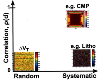
In this context, we can formulate a two-axis system to decompose within-die varia-tion as shown in Figure 2-10(b). As examples, the axes are pre-populated with two of the process steps discussed in Section 2.1, CMP and Lithography. Variation in CMP is largely a result of feature sizes, neighboring features, and pattern-dependencies [27], leading to both highly repeatable (systematic) within-die variation patterns from one die to another, as well as high spatial correlation between devices on a single die. Lithography variation is similar in that it is highly systematic due to mask errors, lens aberrations and other such effects that influence each die in the same manner, but different from CMP variation as the spatial influence of sub-wavelength lithographic systems with OPC is on the order of 1 - 2pm [44].
P,Cov(xx(d) = d) (2.11)
1-.
e.g.
CMP
X3
X2
O4
7E
e.g. Litho
x,
U
I-I0
Random
Systematic
(a) Spatial (distance-dependent) correlation (b) Spatial variation decomposition axes Figure 2-10: Decomposition of within-die spatial variation
measured data from fabricated test-chips.
2.4
Impact to Modeling and Design of Circuits
and Systems
Given the increasing challenge that variation poses to further CMOS scaling, there has been a greater drive to characterize, analyze and better understand the sources of variation as well as their circuit implications.
Complete understanding of the physical processes resulting in certain types of variation is theoretically possible. For example, CMP of interconnect metals is close to a point where it can be modeled accurately enough to substantially reduce layout-induced variations resulting from this unit process [45, 28]. Optical Proximity Correc-tion (OPC) and Sub-ResoluCorrec-tion Assists Features (SRAF) are used in the lithographic
portions of the manufacturing process to reduce uncertainty in the patterned silicon
features. These tools are a result of fairly well understood and modeled optical phe-nomena that occur when patterning features smaller than the wavelength of light used in the lithographic system. However, the decreasing physical dimensions necessary to satiate the industry's desire to further Moore's Law continue to outpace even these

![Figure 2-4: Intel simulation of Random Dopant Fluctuation (RDF) [4].](https://thumb-eu.123doks.com/thumbv2/123doknet/14233867.485915/28.918.228.697.130.336/figure-intel-simulation-random-dopant-fluctuation-rdf.webp)

![Figure 2-13: RazorII latch capable of detecting timing errors and restarting the pipeline [12].](https://thumb-eu.123doks.com/thumbv2/123doknet/14233867.485915/52.918.159.785.136.342/figure-razorii-capable-detecting-timing-errors-restarting-pipeline.webp)