Building an Electronic Drafting Table for Sketch
Recognition
by
Oskar Ernst Bruening
Submitted to the Department of Electrical Engineering and Computer Science
in partial fulfillment of the requirements for the degree of
Master of Engineering in Electrical Engineering and Computer Science at the
MASSACHUSETTS INSTITUTE OF TECHNOLOGY June 2004
@
Oskar Ernst Bruening, MMIV. All rights reserved. The author hereby grants to MIT permission to reproduce and distribute publicly paper and electronic copies of this thesis documentin whole or in part.
A uthor ...
D
tment
... ... . . . . of Electrical Engineering and Computer Science
May 20, 2004
Certified by
Randall Davis
Professor
Thesis Supervisor
Accepted by... 0 MASSACHUSETTS INSgrW OF TECHNOLOGYJUL 2
0
2004
Arthur C. Smith
-airman, Department Committee on Graduate Theses
B
LLding an Electroni PDrafting Table for Sketch Recognition
by
Oskar Ernst Bruening
Submitted to the Department of Electrical Engineering and Computer Science on May 20, 2004, in partial fulfillment of the
requirements for the degree of
Master of Engineering in Electrical Engineering and Computer Science
Abstract
Sketch recognition as developed by the CSAIL Design Rationale Group allows a de-signer to sketch out and test design ideas without the need for complicated CAD programs. An electronic drafting table is required to capture large designs. The design of the electronic drafting table in this thesis uses linear image sensors located in the corners and triangulation to locate the exact position of the pen. The design of the sensors in the corner and the required electronics are explored in detail. We developed, built and tested electronics, proving the feasibility of the design.
Thesis Supervisor: Randall Davis Title: Professor
Contents
1 Introduction
1.1 M otivation . . . . 1.2 The Electronic Drafting Table . . . . . . . . 1.3 Design and Implementation . . . .
2 Designing the Table
2.1 Design Goals . . . .
2.2 Initial Design Approaches . . . .
2.2.1 Indium Titanium Oxide 2.2.2 2-D Camera Tracking . 2.3 Linear Image Sensor Tracking
2.3.1 Motivation . . . .
2.3.2 General Approach ...
2.3.3 The Camera . . . . 2.3.4 The Computing Station 2.3.5 The Display Device . .
3 The Camera Implementation 3.1 The Linear Image Sensor . . . . .
3.1.1 Sensor Requirements . . . 3.1.2 Picking the Image Sensor .
3.2 The Lens System . . . .
3.2.1 Fundamental Optics . . . 18 . . . . 18 . .. . . . 21 .. . . . 21 . . . . 24 . . . . 26 . . . . 26 . . . . 27 . . . . 30 . . . . 33 . . . . 34 36 . . . . 36 . . . . 36 . . . . 37 . . . . 38 . . . . 39 13 13 14 15
3.2.2 Blurring .
3.2.3 Ray Tracing . . . . 3.2.4 Lens Simulation . . . .
3.2.5 Lens Selection . . . .
3.3 The Analyzer Board . . . .
3.3.1 M otivation . . . .
3.3.2 The Intel 80C196NU . . . .
3.3.3 Abstract Block Design . . . . 3.3.4 Detailed Implementation . . . .
3.3.5 The Complete Analyzer Circuit . . . .
3.3.6 Analyzer Design Flaws . . . .
3.3.7 Why the 80C196NU Turned out to be Insufficient
3.4 The Image Sensor Board . . . . 3.4.1 Abstract Block Design . . . . 3.4.2 Breadboard Implementation . . . . 3.4.3 Power Supply . . . . 3.4.4 Changes in the Printed Circuit Board . . . . 3.4.5 Circuit Board Implementation . . . . 3.4.6 Design Flaws . . . .
3.5 External Memory Extension Board . . . .
3.5.1 Motivation . . . .
3.5.2 Board Design . . . .
3.5.3 Programming an External Flash Memory . . . . .
3.6 Softw are . . . .
3.6.1 The Tasks . . . .
3.6.2 The BIOS . . . .
3.6.3 Matlab Data Evaluation . . . . 3.6.4 Java Test GUI. . . . .
. . . . . .. 4 0 . . . 45 . . . 48 . . . 49 . . . 54 . . . 54 . . . 57 . . . 58 . . . 60 . . . 80 . . . 84 . . . 87 . . . 91 . . . 91 . . . 95 . . . 102 . . . 104 . . . 109 . . . 110 . . . 113 . . . 114 . . . 114 . . . 114 . . . 115 . . . 115 . . . 116 . . . 125 . . . 128
4 et-'ELing the CamlerLa 4.1 M otivation . . . . 4.2 Setup . . . . 4.2.1 Camera Arrangement 4.2.2 Camera Placement . 4.2.3 Pen Placement . . . . 4.2.4 Experiment Procedure . . 4.3 Results . . . . 4.4 Conclusion . . . . 4.4.1 Future Considerations 5 Conclusion A Technical Specifications A.1 Analyzer . . . . A.1.1 Memory Configurations. .
A.1.2 Initialization . . . . A.1.3 General Purpose Functions
A.1.4 Points of Improvement . .
A.1.5 Settings . . . . A.1.6 Circuit Schematics . . . .
A.1.7 Bill of Material . . . . A.2 Image Sensor . . . . A.2.1 Settings . . . .
A.2.2 Points of Improvement . .
A.2.3 Circuit Schematics . . . . A.2.4 Bill of Material . . . .
A.3 Memory Extension Card . . . . . A.3.1 Circuit Schematics . . . .
A.3.2 Bill of Material . . . .
A.4 Power Supply . . . .
137 137 138 138 139 140 141 142 146 146 150 152 152 . . . . 1 5 2 . . . . 1 5 3 . . . . 1 5 4 . . . . 1 5 5 . . . . 1 5 6 . . . . 1 5 6 . . . . 1 5 7 . . . . 1 5 7 . . . . 1 5 7 . . . . 1 6 1 . . . . 1 6 1 . . . . 1 6 7 . . . . 1 6 7 . . . . 1 6 7 . . . . 1 6 7 . . . . 1 6 7
A.4.1 The Connector.... ... . . . . . . . . . . . 167
B Tools 173 B.1 Software Design Tools . . . . 173
B.1.1 Assembler "mca96" . . . . 173
B.1.2 Linker "mclink" . . . . 173
B.1.3 Script "asmall" . . . .. 174
B.1.4 Script "intelhexshift.pl" . . . .. 174
B.1.5 Program mkrom.c . . . . 178
B.2 Hardware Design Tools . . . . 178
B.2.1 Protel DXP . . . . 178 B.2.2 ExpressPCB . . . . 180 C Getting Started 181 C.1 Resources . . . . 181 C.1.1 Equipment . . . . 181 C.1.2 Books . . . . 183 C.1.3 Companies . . . . 183
C.2 W riting Assembly Code . . . . 184
C.3 Programming the Image Sensor Board . . . . 185
C.4 Lessons Learned . . . . 186
C.4.1 Electrical Concerns . . . . 186
C.4.2 Circuit Schematics . . . . 187
C.4.3 Circuit Layout . . . . 188
List of Figures
1-1 The final design of the drafting table . . . . 2-1 The complex ITO network . . . . 2-2 Testing IT O . . . .
2-3 Two sheets of coated with ITO, separated by spacer dots .
2-4 The 2-D camera tracking the movement of the pen . . . . 2-5 Two sensors locate the pen using triangulation . . . . 2-6 A cylindrical lens focusing the light of the pen on the image 2-7 Logic diagram of the camera components . . . . 2-8 2-9 3-1 3-2 3-3 3-4 3-5 3-6 3-7 3-8 3-9 3-10 3-11
Logic diagram of the computational station. Two possible placements for the projector
How the lens focuses the light . . . . The focal length of a lens . . . . The two causes of blurring . . . .
Different focal points moving along the center ray Geometric diagram of the blur problem . . . . Raytracing - The basic variables . . . . Raytracing Simulations . . . .
Regular lens vs. cylindrical Lens . . . . Different Lens Simulations . . . . The microcontroller building blocks . . . . Using a demultiplexer to save Chip Select lines . .
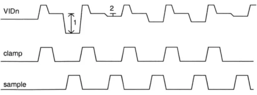
. . . . 23 . . . . 25 . . . . 26 sensor . 32 . . . . 33 . . . . 34 . . . . 34 . . . . 39 . . . . 39 . . . . 41 . . . . 42 . . . . 43 . . . . 47 . . . . 49 . . . . 50 . . . . 53 . . . . 59 . . . . 69 3-12 Timing diagram for sampling the output for the linear image sensor
. 16
. 22 . 22
Tetingu111 thl TIS1U8L2oLL using a square Vave as input . . .
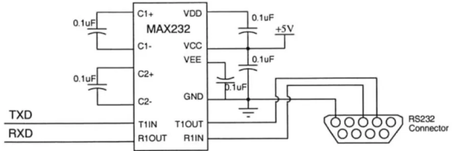
Connect TXD and RXD to the serial port with MAX232
3-15 Example of the BIOS serial communication 3-16 3-17 3-18 3-19 3-20 3-21 3-22 3-23 3-24 3-25 3-26 3-27 3-28 3-29
3-30 The pen's range as located by the 3-31 Screenshot of the GUI . . . .
Experiment setup . . . . . Pen positions . . . .
Measurements for line A Measurements for line B Measurements for line C
Visualization of the results
Analyzer jumper locations Analyzer board schematics Analyzer board schematics
(1/2) (2/2)
three algoril
- Analyzer . .
- Input buffers
A-4 Image sensor board setting
The 40 pin connector of the extension port . . Logic analyzer snapshot of the addr./data-bus Correct implementation of an I/O port circuit Complete circuit diagram of the analyzer . . .
The different section of the analyzer circuit . . Simple digital control logic . . . . Control signal timing diagrams . . . . The final schematics of the input buffers . . .
Complete output buffer circuit . . . . Three power supply circuit . . . . The final digital board . . . . The final analog board . . . . Image sensor output stabilizer circuit . . . . . Visualizing the image sensor output . . . .
139 140 143 144 145 147 156 158 159 160 ') 19) 3-14 3-14 71 75_-75 . 4-1 4-2 4-3 4-4 4-5 4-6 A-1 A-2 A-3 . . . . 76 . . . . 77 . . . . 77 . . . . 80 . . . . 8 1 . . . . 8 2 . . . . 93 . . . . 98 . . . . 100 . . . . 102 . . . . 103 . . . .111 . . . .111 . . . . 113 . . . . 129 thm's . . . . 131 . . . . 136
A-5) ImageL1: s nsor scheatics,, (1/5) Coneto . . . . . . . . . . . . . . . . Z12
A-6 Image sensor schematics (2/5) - Control logic . . . . 163
A-7 Image sensor schematics (3/5) - Input buffer . . . . 164
A-8 Image sensor schematics (4/5) - Output buffers . . . . 165
A-9 Image sensor schematics (5/5) - Voltage regulator . . . . 166
A-10 Memory extension card schematics . . . . 170
A-11 The 4-pin power connector . . . . 171
List of Tables
2.1 Summary of the different implementation possibilities. . 30
3.1 Lens properties and simulated results . . . . 52
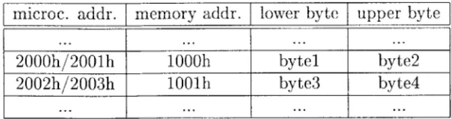
3.2 Example of 16-bit instruction memory . . . . 62
3.3 Using address shifting to use the full 16-bit memory . . . . 63
3.4 Section labels for Figure 3-20 . . . . 83
3.5 Fixed voltage requirements for image sensor inputs . . . . 101
3.6 BIOS software download error codes . . . . 119
3.7 BIOS commands . . . . 121
3.8 Examples of the different BIOS library functions . . . . 126
4.1 Distances of the measurements points to the camera . . . . 141
4.2 Settings and results of the experiment . . . . 147
A.1 A.2 A.3 A.4 A.5 A.6 A.7 A.8 Microcontroller memory partitions on the analyzer board Instruction memory segmentation . . . . Bill of material for analyzer board . . . . Bill of material for image sensor board (1/2) . . . . Bill of material for image sensor board (2/2) . . . . Bill of material for memory extension card . . . . Color code for power supply connector . . . . Bill of material of power supply connector . . . . 152 153 160 168 169 169 171 172 B.1 Example assembler configuration file . . . . B.2 Example linker configuration file . . . . . . . . 175
C. I Equipment shopping list from Jameco . . . . 182
C.2 Equipment shopping list from Digikey . . . . 182
C.3 Equipment shopping list from Newark . . . . 182
List of Algorithms
1 Sending a byte stored in the AL register . . . . 74
2 Receiving a byte and saving it in the AL register . . . . 74
3 Finding the pen - first approach . . . . 129
4 Finding the pen - second approach . . . . 130
5 Finding the pen - third approach . . . . 132
Chapter 1
Introduction
1.1
Motivation
In today's world, as designs become more and more complicated, it is increasingly more difficult to capture the design rationale, even with advanced design tools. This means that, in the end, the design of a product is known, but not what design decisions have been made on the way and why. This information is the design rationale. In software engineering, as in any other engineering field, it is vital that the design be carefully documented in order to be able to make changes to it. For the designer, this is time-consuming overhead and it is not the original designer, but succeeding ones, who benefit from good documentation in order to make changes. Therefore, documenting the rationale is often more trouble than it is worth for the original designer.
This is the motivation behind the Design Rationale Group. The main idea is to create new low overhead ways for designers to capture their rationale while in the design process. The capture process should be less trouble than it is worth. Engin-eers and designers, in general, are very enthusiastic about describing their designs, especially to a fellow designer. It is the tedious process of writing everything down that kills the excitement. If it were possible for a machine to capture the natural human way of describing a rationale, the problem would be solved as the designer would have more time to devote to explaining the design.
The g.al "f +h- TheDCesig Patirrnlet (rnip is t bhiiill n system in which the designer
can sketch, talk and gesture with the computer as if he were talking to another designer. The designer works in a design environment with embedded intelligence, allowing designers to work in familiar ways in familiar media (e.g., white boards), yet give those media new and powerful capabilities (e.g., the ability to understand a sketch, ask intelligent questions about a design, etc.). This offers the possibility of making rationale capturing an almost effortless and incidental byproduct of design.
1.2
The Electronic Drafting Table
The Design Rationale Group currently uses Acer tablet PCs and Mimio whiteboards for sketch recognition. Unfortunately, these devices are insufficient. The tablet PCs, meant as an alternative to conventional paper notebooks, allow the user to draw with a pen-like stylus directly on the screen. But compared to the drafting tables used
by professional designers (the target group of the DRG's project), the tablet PC is
simply too small.
Mimio white boards are one alternative. The Mimio white-board system consists of a base station and a marker equipped with ultrasound and infrared (IR) electronics. When the user starts to draw a stroke, the pen sends an IR signal to the base station. The pen then emits an ultrasound signal which is picked up by two sensors on the base station. By measuring both, the time difference between the IR signal and the ultrasound signal and the delay of the ultrasound signal reaching each of the sensors, the base station can triangulate the position of the pen. Using this technology, Mimio whiteboards overcome the problem of size. However, the Mimio is also insufficient as it does not offer high resolution. It is an electronic replacement for marker pens used on typical, large white-boards. What we were looking for, however, is the electronic equivalent of a pencil and a large sheet of paper.
1.3
Design and Implementation
My project was to first design and then build an alternative to the tablet PC and
the Mimio white-board, combining the best of both worlds: the high resolution of the tablet PC and the large size of a drafting table.
After considering and testing different designs, it became apparent that this task was much more difficult and complex than I had anticipated. The initial design used a material called Indium Titanium Oxide (ITO), which is often used for touch screens (e.g. the Palm Pilot). The disadvantages of ITO are the low resolution, limited size and slow response, while the main advantage is the relatively simple implementation.
My initial design was based on the assumption that I would be using ITO, but
initial testing showed it to be insufficient for the task: the noise levels were much too high, causing inaccuracies if it were used as an interface. The pointer would jump around, independent of stylus movements.
The next idea was to place a digital camera underneath the table. The pen would glow and all the camera had to do was to track the light as it moved. This idea, too, proved unsuitable. The main problem here was that a camera fitting the requirements (high speed and high resolution) does not yet exist. Even if it did exist, the signal processing of camera output would require extremely fast processors, which are unavailable. So either way, this approach proved infeasible.
The final design approach involved using four cameras, one in each of the four corners of the screen (Figure 1-1). The advantage here is that each camera needs to scan only one dimension. While we require four cameras, each one has to process only a fraction of what the camera underneath the table would have had to process. But reducing the amount of data to be processed also adds to the complexity. New problems, such as blurring, appeared: placing the camera in the corner meant that the pen could be very close or very far away.
With the goal of completing the whole table, I tried to address these issues and outline solutions as I began the implementation. Unfortunately it was not possible to complete a working prototype in the time available in part because of
signific-Pen with bright glowing tip
Projector
Figure 1-1: The final design of the drafting table
ant errors in the data sheets of chips in the camera design. The final result of my implementation is a working model of the corner camera and its electronics, which are capable of tracking the pen moving left and right. I used this camera to test a fundamental question: is this approach, as I had envisioned it, feasible? The answer is yes. This thesis covers the design approach, design decisions, implementation of the first camera, and discusses problems encountered.
On a personal note, the whole process has been an incredible learning experience for me. I started off thinking I knew more than enough about hardware since I had taken MIT's digital laboratory class and microcontroller laboratory class and done very well in them. I was wrong. My initial implementations were poor. One time, it took me one and a half months to find a single bug. The design mistake was very subtle and I will never make this mistake again. Many more problems revealed themselves, each of which were very frustrating. Finally (sometimes after weeks), I would find the source and fix it. And then the next problem would occur. Overall, however, the project was a great learning experience. I had to tackle problems from a broad range of engineering fields, such as optics (for the corner camera), mechanics (for the physical table itself), analog and digital hardware (for the camera circuit
Chapter 2
Designing the Table
This chapter covers the design of the drafting table, explaining the design goals, industrial alternatives, the initial design attempts and the final approach.
2.1
Design Goals
"Just like pencil and paper on a real drafting table." That was the motto of the project. The drafting table was supposed to convey the feeling of real paper, while really drawing on a computer. The pen should allow the user to draw very thin lines, just like a pencil. The designers are supposed to use the drafting table as a real tool to express their ideas. If possible, the pen should also be pressure sensitive, giving the user the capability to draw thin or thick lines. The table - once it is designed, built and working - should also be relatively cheap to reproduce.
To reach this goal we had to satisfy a number of criteria.
Size. The designer should not be limited to a notepad size surface. We would like
to give designers a real-world drafting table similar to those they would encounter at their own office, which means the table would be about the same size as the non-electric version. We set the target size of surface of the table to 1.0 x 0.75m. This is large enough for designers to work on and it reflects the 4:3 ratio between width and height. This ratio is also found on computer screens and would allow us to use generic computer displays, such as a projector or large LCD screen.
PrrjeUtur IUUation. BeU~dse wU Use a U1t11eUrA1 Cs an interf-1act, VVw neu tU
project the computer screen onto the drafting table, so the designer feels like he is drawing directly on the table. As we try to imitate a real drafting table as much as possible, we have to take into account that any line drawn has to be visible at all times. If we were to place the projector somewhere on the ceiling for example, the shadow of the user's arm would hide parts of the drawing. Therefore, the display device had to be placed underneath the table.
Line width. When drawing with a pencil the line can be very thin. The drafting
table should reflect this, so we need high resolution. The initial target resolution was about 2,000 x 1,500 pixels. Using the size of the table of 1.0 x 0.75m the size of one pixel would then be 0.5mm. This is equivalent to saying that the thinnest line possible will be 0.5mm wide, which is very close to pencil resolution. This would be the ideal goal. It might turn out, however, that for technical reasons it is not possible to reach this resolution. In this case the minimal resolution acceptable would be the resolution of the projector - typically 1024 x 786. If our tracking resolution was smaller than this, the size of the pen point would cover several pixels on the screen, which is unacceptable. Once again we would have a marker, not a pencil. At a minimum resolution of 1024 x 786 pixels moving one pixel on the surface would correspond directly to moving one pixel on the computer screen. In this case, on a 1.0 x 0.75m drafting table surface, one pixel will correspond to the size of about 1mm. This is relatively large, but it would still be acceptable.
Small, cordless pen. A wire running from the pen is not very desirable, as it
limits the way the designer can draw. Similarly, a pen packed with electronics of the size of a cell phone would also be limiting.
Transparent surface. If the display is to be underneath the surface, the surface
must be transparent. This significantly limits the technologies that can be used to locate the pen. In the past four decades many technologies for pointer interfaces have been developed, but most of them are separate from the computer screen. In a graphic tablet, for example, the user draws on one surface, and sees the motions of the pen on a separate computer screen. In our case we want to track the pen's motion
on tile screen itself anu only receVntly hiave uchoLge U'U11 dV p to) sIU" 1Uort this idea (e.g. tablet PC, Mimio). As the current technologies seem to be inadequate
for our task, we had to come up with some technology of our own. Thus the main question of this project turned out to be "how do you track the pen?"
One option is a touch sensitive surface, as for example used in graphic tablets. However, the particular touch sensitive surfaces used in these graphic tablets are not transparent and therefore not suited for the project.
PDAs and ATM machines offer examples of transparent touch sensitive surfaces, using indium titanium oxide (ITO) technology to detect the touch on the screen. However, ITO turned out to be too noisy and usable only with small surfaces.
The alternative is some kind of wireless communication. There are a range of different options here. The Mimio whiteboards use ultrasound to locate the position of their pen, with receiver stations located at different corners measuring the time it takes for the signal to reach the sensor. Tablet PCs work in a similar fashion. Tiny antennas send out an RF signal and the stylus has a spring inside, which is compressed when the stylus touches the drawing surface. Depending on the compression of the spring the signal is distorted differently. Sensor pick up that distorted signal and can figure out where the pen is located and how hard it is being pressed on the surface.
Finally, very simple, low resolution touch screens have light emitting diodes (LED) placed along one side of the screen and photo sensors on the opposite side. Touching the screen interrupts the beam of light. The position of the contact can be determined on one axis, by looking at which photo sensor has lost contact with its partnering
LED. The exact position of the touch can be located, by placing the same setup of
LEDs and photo sensors along the other two edges of the screen.
Each of these solutions comes with limitations. The goal of the project was to use one or more of these technologies or develop a novel approach to track the pen. This turned out to be the most difficult part.
2.2
Initial Design Approaches
This section covers initial attempts to solve the problem of pen tracking and shows a few dead ends I encountered before coming up with my final design. The dead ends show how I came to the final design approach.
2.2.1
Indium Titanium Oxide
Previous work on this project had focused on using indium titanium oxide (ITO), making it a natural starting point.
Indium titanium oxide is a clear substance, which can be coated on a plastic sheet and provide constant resistivity over the area. If you place a voltage source along one side of the sheet and a ground on the other, current will flow uniformly from one side to the other. It is the only clear substance to have that property, leading us to try using it for tracking the pen.
One scenario is easy to envision: if the pen emitted 5V constantly and you place voltage sensors along the sides of the sheet you should be able to detect the pen's position. The voltages measured on each side would correspond to the distance of the pen to the sensor. This sounded very straightforward.
However, some simple testing indicated that ITO had several fundamental flaws that were not apparent initially.
" ITO is coated onto plastic: ITO sheets are plastic with only a thin layer of
ITO coated onto it. This turned out to be problematic, because moving a pen across the sheet scratched the thin ITO layer, changing the electric properties of the ITO dramatically. Current would flow unpredictably across the sheet.
*
ITO is a complicated network: The original plan was to use the pen as a 5V source and then measure the voltages at the corners. This, too, provedmore complicated than expected. Current would not flow equally from the pen's point to the corners as expected. The explanation is clear when visualizing ITO as a complex network of resistors. The current flow is very hard to predict in
5V
...* , ... ... sesr
sensors s- sensors
Figure 2-1: The complex ITO network
flow of current
Iteter
a. The setup b. Ideal voltages c. Measured voltages
Figure 2-2: Testing ITO
this complicated network, especially since we know very little about the current flow inside the material. Scratches and material flaws complicate this even
more. Figure 2-1 illustrates this problem.
ITO is noisy: To avoid the complex network problem, I applied a high voltage
on one side of the sheet and a ground at the opposite side. Current, in this case, should flow equally across the sheet. All the pen would have to do is to measure the voltage at any given point. The distance from the side with the applied voltage should be linearly related to the voltage measured at the pen's position. A series of tests produced very inconsistent results. The measured voltages differed from the predicted voltage by up to 0.3V (Figure 2-2) . This would translate to an error of 30 pixels, or almost 3 cm on the drafting table, and was unacceptable.
In addition, a wire would have to be run from the pen to the drafting table, limiting 22
theu usability Uf the table.
Despite all these problems, ITO is still successfully used for touch screen applica-tions in industrial environments. The most commonly used touch screen technology using ITO are so called resistive touch screens. I did some research on the topic to figure out how the industry overcomes these problems.
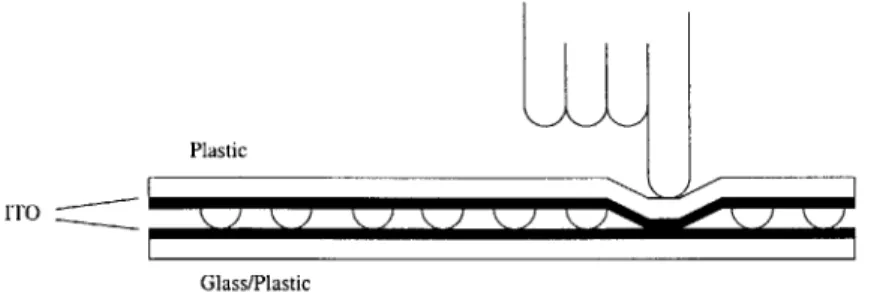
" ITO is coated onto plastic: Industrial uses of ITO involve two sheets of
plastic with ITO on the inside, separated by spacer dots (Figure 2-3), which are tiny plastic dots covering the whole sheet. When a user touches the screen, the dots get compressed at that point, the two sheets connect and current flows. From the flow of the current the position of the pen can be determined.
" ITO is a complicated network: The commercial solution to this problem is
the same I used: instead of placing a single point voltage source on the ITO sheet, the whole side of one sheet is connected to power, while the other is
connected to ground. This way current flows uniformly across the sheet.
" ITO is noisy: There is no real solution to this problem. Using complicated
signal processing, the noise is cancelled out as much as possible. However, the use of ITO remains limited. Currently the maximum screen size of industrial touchscreen is 19" diagonally with a maximum resolution of 1000x1000 pixels.
Considering the fact that companies have spent a lot of resources to reach this size and resolution, it appears that current size of ITO touch screens (up to 19") is the physical limit. Moreover both the size and the resolution are insufficient for the drafting table.
Plastic
ITO
Glass/Plastic
There are two mr pp h 1 for tcTih screens, also iing ITO, which are
worth mentioning: capacitive touch screens and surface acoustic wave touch screens.
However, it should be noted that neither improves on the resolution or size of the resistive touch screen.
* Capacitive touch screens: In this case, glass is fused with an ITO coating
and the coating is connected to four electrodes in the corners. These electrodes produce an oscillating wave signal. When touching the screen, the person's body changes the impedance of the system. This change in impedance can be measured and the location of the touch determined. The maximum resolution achieved using this approach is 1000x1000 pixels.
e Surface Acoustic Wave touch screens (SAW): In this case acoustic wave
signals are transmitted across the surface of the sheet and reflected at the op-posite side. When the user touches the screen some of the energy of the wave is absorbed and the position of the pen can be located by measuring the delay of the wave. The approach is limited, however, to a resolution of 900x900 pixels.
2.2.2
2-D Camera Triacking
After the idea of using ITO failed a new design had to be developed. One idea was to have the pen emit some signal to a base station. When the pen moves, the signal would shift and the change could be measured and turned into coordinates. This approach, however, had been implemented by the Mimio white-board system and provided insufficient resolution. Because my experience in the field of signal processing was limited, I did not try to improve on the Mimio design and instead looked for a simpler alternative.
The next design used a camera placed underneath the table. This required a camera with high resolution (2,000 x 2,000 pixels) and a frame rate of at least 133Hz (the sampling speed of an ordinary computer mouse). The color depth was not as
1A good summary of the different touch screen technologies can be found at [11] (http: //www. norteng. com/tchselgd .html)
screen
camera
Figure 2-4: The 2-D camera tracking the movement of the pen
important, because all we needed to do was find a bright spot (the pen) moving across the surface (Figure 2-4). Four bits or fewer would be sufficient for the task.
I spent several weeks trying to find this kind of high resolution, high speed, low
depth camera, but I did not find one. Basic mathematics indicated why - the data rate was too high!
(2000 x 2000pixels) x 200Hz = 800,000, 000 pixel
second
Assuming that such a camera existed and if my digital signal processor (DSP) required only a single instruction to analyze a pixel, the processor would have to run at 800MHz - a speed that the fastest DSPs barely reach. In reality, evaluating each pixel would cost more than one instruction, even in the simplest case, as reading the pixel's value is one instruction by itself. You would also have to find an analog-to-digital converter that can sample at 800MHz. Currently the fastest analog-to-analog-to-digital converters can sample at 70MHz. Finally, on most DSPs the time to execute an instruction varies with the type of instruction. Many instructions take several clock cycles. And even if we were to reduce requirements by setting the resolution to 1024x786 pixels and the sampling rate the 133Hz, we would still have to sample at around 110MHz.
The bottom line is that this was simply not possible with today's technology. A different solution had to be found.
Figure 2-5: Two sensors locate the pen using triangulation
2.3
Linear Image Sensor Tracking
2.3.1
Motivation
Inspired by the idea of using a camera for tracking the pen, I decided to keep working in that direction. The goal was to reduce the amount of data that had to be processed. Placing a 1-D camera in each of the four corners of the screen was the solution. A 1-D camera is simply a row of photosensitive pixels. These so called linear image sensors are commonly used in scanners and fax machines. Image sensors would be placed in the corners, scanning just above the surface of the table, detecting a pen that would glow brightly. The image sensor can then locate the angle between the pen and the image sensor. By taking two sensor's angles we could triangulate to locate the pen's position (Figure 2-5).
The advantage is that instead of having to process 2, 000 x 2, 000 = 4, 000, 000 pixels, we would have to process only one row of data, e.g. 2, 000 pixels. Since this is three orders of magnitude less, we can even increase the resolution to 10,000 pixels without coming anywhere near the technical limitations we found when using the 2-D camera. This approach is, from the technical point of view, feasible using today's technology.
Using two cameras (linear image sensors) and triangulation to find the position, however, also adds another layer of complexity. When using the 2-D camera we could read the location of the pen right from the position of the bright spot on the camera. When doing triangulation we need to compute the findings of two image sensors to find the pen's location. We need to be able to do these computations relatively fast
- at least 200 times per second.
frUIIm lte dIltea. VVIti pCLA11g a 2-1L' c-amer'laa udrneat11 UC JAh UL1- h pn.ld
always be at almost the same distance from the camera. This is important, because ideally, for maximum performance, we should have the pen in focus. To do this, using the linear image sensor, the lenses would have to adjust depending on how far the pen is away - identical to the auto-focus function in a regular camera. As it turns out, auto-focus is not an option as it is too slow.
After careful consideration and looking at similar industrial solutions based on the same idea, we determined this approach to be the most promising one.
2.3.2
General Approach
The problem can be broken down into several functional blocks.
" Image Capture: The first component is the camera. Here the 1-D image is
captured and the raw data transmitted to the next component. The camera itself consists of the lenses, the linear image sensor, the electronics controlling the image sensor and an interface section allowing us to transmit the raw data to the next stage.
* Image Data Conversion: The output of the linear image sensor is an analog
signal corresponding to the brightness of the current pixel. A low voltage means a lot of light, while the high voltage corresponds to darkness. In order to process this data it needs to be digitized. This is the function of the image data converter does.
" Image Data Analysis: Once the signal has been digitized the image can be
analyzed. In practice, this means we have to find the angle of the pen to the image sensor.
" Triangulation: The angle of two cameras is combined to find the pen's absolute
location on the table.
into tht rltiuve locationl Wf ut Pun U1n theu scremi. t this"! puint the mous
pointer should be located right underneath the pen.
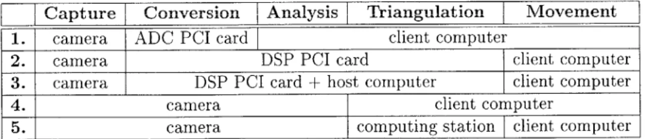
Based on these functional blocks we have different possibilities for implementation. There are only two constants. First, the image capturing has to be done on the draft-ing table itself, since this is where the sensors need to be located. Second, the mouse movement needs to be done with a driver on the client computer, since the computer is connected to the display device and only the computer can do the transformation between absolute surface position and relative screen position. Otherwise there is a lot of flexibility in how to implement the remaining blocks. The following list gives an overview over the most feasible possibilities.
1. Place an analog-to-digital converter (ADC) card into a PCI slot of the client
computer. This card will do the data conversion for all four corner cameras, then the client computer will do the image data analysis and the triangulation.
Advantage: Besides the camera, there is no need for additional customized
hardware. The ADC card can be purchased off-the-shelf.
Disadvantage: Assuming 10,000 pixels per image sensor, the PC has to analyze
40,000 pixel per sample (40, 000 x 200 = 8, 000, 000pixels
/
second) and do the triangulation while running the operating system and client software. This is a lot of overhead just to move the mouse.2. Instead of placing a simple ADC card, we could place an ADC card with built-in high speed digital signal processors (DSP) in the client computer.
Advantage: The DSP can do the conversion and analysis of the data, maybe
even compute the absolute location of the pen. The overhead would therefore be removed from the client's CPU to the DSP card. Also, the DSP card would be off the shelf, which would reduce the amount of effort spent on designing hardware.
Disadvantage: By using a special card located in the client computer, only that
computer can be used for sketch recognition. Ideally, however, anyone should be able to bring in their computer, install a driver and connect to the table over
TTOT-) V-- A I-- 1:-I4. -- - T-NOTD A - -- 4 f--
*-U3D, fr tXamplit. Ls ig, 11, speu IJkI cads ad 1te sulvvtal LU pIUgamld
them are expensive (at least $5,000-$6,000 each).
3. Place a high speed DSP card in a dedicated host computer. This computer
and the DSP card would do everything up to the computation of the absolute surface position. The client computer can then connect to the host computer over e.g. USB to use the table.
Advantage: A separate client computer can be used. Only little customized
hardware is required (camera).
Disadvantage: Extra computer required in addition to the expensive DSP
board.
4. The camera also does the analog-to-digital conversion and the image analysis and the result is sent to the client computer over USB, which then does the triangulation and moves the mouse.
Advantage: All the high speed data processing is happening at one place (the
camera). The client only needs to do triangulation 200 times
/
second.Disadvantage: Camera electronics are more complex, since the task is more
complicated. Furthermore, the client computer needs to be connected to all four cameras separately. This would require four free USB connections to drive the mouse. Even with a USB hub, the software would still have to deal with four separate ports. Finally, calibration of the camera sensors would have to be done on every single client computer, which might be complicated and aggravating.
5. The camera does the analog-to-digital conversion and the image analysis and
the result is sent to a computing station, which collects the input from all four cameras and computes the absolute surface location of the pen. This information is then transmitted over USB or serial connection to the client computer.
Advantage: The computing station can do the calibration and triangulation.
The client computer could therefore just plug in and work. In addition this would cause minimal overhead on the client's side to move the mouse.
Capture Conversion Analysis Triangulation Movement
1. camera ADC PCI card client computer
2. camera DSP PCI card client computer
3. camera DSP PCI card + host computer client computer
4. camera client computer
5. camera computing station client computer
Table 2.1: Summary of the different implementation possibilities.
Disadvantage: In addition to the complex electronics of the camera a second
piece of customized hardware (computing station) would have to be designed.
An overview of the different possibilities is summarized in Table 2.1. After considering all the options, I decided to go for the last option. Choosing this option would allow us to test the general design approach of placing cameras in the corners without having to spend $12,000 (e.g. DSP card and software) on equipment. Secondly, having all the complex electronics for the camera at one place, at the camera, minimizes the number of components while keeping the high speed components together. This also eliminates problems that high speed communication might cause. Finally, the drafting table would be one complete piece of equipment that could be connected to any PC over the USB or serial port.
2.3.3
The Camera
As mentioned before, the camera takes over several functions. Not only does it capture
the picture itself, but it also analyzes it and tries to find the pen's angle. All this needs to happen at a very high speed, since each picture consists of 10,000 or more pixels and 200 pictures have to be taken per second. Keeping this in mind, the camera consists of the following subcomponents:
* Lens system: The goal of the lens system is to keep a relatively sharp image of
the pen, at all distances. The lens system has to be fixed focal length, since any
auto-focus mechanics would be too slow (the auto-focus would have to adjust the lenses within I 200 of a second).
" Linear
image S
s Th. s is the actual chip that takes the picture. Thechip receives a set of control signals and sends out the pixel values of the image one after the other.
" Control Electronics: The component receives a "start" signal and sends out
the control signals through the input buffer to the image sensor to take one complete picture.
" Input Buffer: The output of the control electronics is buffered and passed on
to the linear image sensor.
" Output Buffer: This section takes the raw, analog pixel values as they come
from the linear image sensor and sets them up for the analog-to-digital conver-sion.
" Output Converter: The buffered analog value of the current pixel is converted to a digital value.
" Analyzer: The analyzer takes in the digital value of the pixel and tries to
figure out what the angle to the pen is.
" I/O Port: The I/O port communicates between the computing station, the
analyzer and the control electronics.
The lens system is separate from the other parts, as it is the only non-electronic component. The lens is used to focus the light emitted by the pen at one location on the image sensor. Since we read in only one dimension, we should use a cylindrical lens. The focused light of the pen is then, ideally, only a bright, fine line on the image sensor. Figure 2-6 illustrates this idea. The location of that bright spot on the image sensor then corresponds to the angle at which the pen is located. As we move the pen, the line moves along the image sensor.
The mapping of pixel number to angle is not linear, because the image sensor is flat. The pixel-to-angle mapping needs to be created at run time using some kind of
Figure 2-6: A cylindrical lens focusing the light of the pen on the image sensor
calibration tool. The analyzer can then use the stored conversion map to analyze the picture.
In operation the drafting table would have to take the following steps roughly 200 times per second (Figure 2-7):
1. The computing station sends a "start" signal to each of the four cameras. This
signal tells the camera to take a picture now.
2. The "start" signal goes through the I/O port on the camera to the analyzer.
3. After checking whether the previous picture run has been completed, the
ana-lyzer sends the "start" signal to the control electronics.
4. The control electronics start sending signals through the input buffer to the linear image sensors and the output converter.
5. The linear image sensor takes the pictures and sends the value pixel by pixel to
the output buffer.
6. The output buffer passes the pixel values on to the output converter.
7. The pixel value is converted to a digital format by the output converter and
passed back to the analyzer.
8. The analyzer collects the incoming pixels and tries to find the pen in the image. 9. The location of the pen is sent back to the computing station.
32
image sensor
0 lens
computing station
1/0 port camera
control elcrnic input buffer
analyzer image sensor|
output converter (_. output buffer
Figure 2-7: Logic diagram of the camera components
2.3.4
The Computing Station
The computing station is relatively simple in design. All it has to do is to collect the angle at which the pen was located on each of the cameras, triangulate and send the information on to the client PC. Since the position of the pen is updated at 200Hz, the triangulation needs to be done only at 200Hz, which is relatively slow.
Triangulation requires the computing station to take the tangent of the angles. Taking the tangent, however, is a complicated mathematical function and not easily implemented. It is therefore easier to pre-compute these values and store them as a lookup table in the memory of the computing station. Pre-computing these values also reduces a significant amount of overhead and increases significantly the speed at which triangulation can be done. Overall, the processing unit on the computing station can be run at relatively low speed to fulfill its purpose.
Taking this into account, the computing station then consists of the following subcomponents (Figure 2-8) :
* I/O Ports: The computing station needs four I/O ports to communicate with
each of the four cameras.
" Computational Unit: Here the returned values from the cameras are
evalu-ated and the absolute surface location of the pen calculevalu-ated.
" Mathematical Look-up Memory: Complicated mathematical functions are
precomputed and stored in this memory.
" USB/Serial Port: Once the location of the pen has been determined, it is
/ p B computational unit USB/Serial port
1/0 port C
mathematical
1/0 port D lokupmmry
Figure 2-8: Logic diagram of the computational station
2.3.5
The Display Device
Since high quality display devices, such as LCD screens and projectors, are readily available in many different size with different features, it is much more economical and feasible to buy one than to build one. The display device should be located conveniently underneath the screen. The initial design uses projectors, since these
are relatively cheap and can be connected quickly to any client computer.
The main problem with using projectors is that they require, of course, space between the projector itself and the surface they display upon. This projecting dis-tance depends on the projector and the lenses it uses. However, it is rare to find a projector where this projecting distance is less than 1.5m. In this case this would mean that the drafting table is at least 1.5 m high, which is unacceptable. The simple solution is to place a mirror underneath the table and place the projector behind the table. If a projector can be found where the projecting distance is small enough, the projector could be placed underneath the table, otherwise a mirror would reflect the image from the projector behind the table. Figure 2-9 illustrates these two options. An LCD screen, of course, would not require this set up. However, these screens, especially in the given size, are currently very expensive.
Option 1 Option 2
surface surface
-.. .
prjet fioor level
mirror
projector floor level
No matter which d0 1is A ie is st will simply connet tn the video output of the client computer. The client therefore sends its screen image to be displayed on the drafting table and the drafting table is then simply an extension of the client. This allows for maximum flexibility, as any user can bring in their own
Chapter 3
The Camera Implementation
Once the design of the drafting table had been established, I started implementing the camera to test the feasibility of the approach. This chapter covers the implementation of the camera and the related test results.
3.1
The Linear Image Sensor
The first step was to select a linear image sensor, as all other requirements depend on the selection of this sensor. The optics relied on the physical size of the sensor and its capabilities; the control electronics had to be designed to send the right control signals to the image sensor; the buffers, converters and analyzer had to match the speed of the image sensor.
3.1.1
Sensor Requirements
There are two main requirements for the image sensor: speed and resolution. Speed is important because we would like to sample at 200Hz. This means if the sensor has
1,000 pixels it needs to be able to run at 200 x 1, 000 = 200KHz minimum data rate. Resolution is important since we want to track the pen with pencil accuracy and even slight movements of the pen make a difference. The image sensor should be able to detect these differences. I decided that 2,000 pixels would be the absolute minimum
and ",uuu pixels an' above would be desirab'e.
Color would also be useful, as it would allow us to assign different functions of the pen (drawing vs. erasing) to different colors. But this is a feature that can be ignored if the image sensor satisfying the first two requirements is a gray-scale image sensors.
3.1.2
Picking the Image Sensor
There are two types of image sensor technologies: CMOS and CCD. CCD (charge-coupled devices) image sensors were the first to be developed and are slightly older. Later, CMOS (complementary metal oxide semiconductors) technology, such as used in integrated circuits, was applied to the field of image sensors. The advantages of
CMOS over CCD are mainly the reduced power consumption and lower production
costs. Currently, only expensive linear image sensors based on CCD technology are available ($700-1,000 per sensor). However, in the future, it might be possible to switch to cheaper CMOS sensors.
The main companies involved in linear image sensor development are NEC, Kodak and Atmel. Research on each of the chips and discussions with company represent-atives provided the following conclusions:
" NEC: At the time, it was hard to find information about the NEC's chips.
They seemed expensive (> $1,000) and had a low resolution (< 5,000 pixels). This may have changed as I now find1 sensor chips with a resolution of up to
7,000 pixels in gray-scale and up to 10,000 pixels for color.
" Atmel: The main chip that looked like an option was the TH7834C, a
gray-scale linear image sensor with 12,000 pixels (2.4MHz minimum data rate). The
chip has four outputs pins. This means the values of four pixels are passed out at the same time. The analyzer would have to grab all four pixels at the same time. This is possible, but not the most desirable option, as reading sequentially is easier. Getting a quote on the chips for small quantities (4-5 chips) turned
out to be very difficult. The final price, after talking to several different people
at Atmel, was $890 for each chip.
o Kodak: Kodak seemed to have a wide variety on color linear image sensors2
The KLI series (Kodak Linear Image) ranges from 2,000 pixels to 14,000 pixels (2.8MHz data rate). Interestingly enough all the chips had the same price, $780,
independent of speed or resolution.
The final choice was the Kodak KLI-14403. It has the highest resolution, the required
speed, comes in RGB colors (red-green-blue) and costs less than NEC and Atmel's alternatives.
As the project continued it turned out that, although the chip itself was working perfectly and suitable for the project, the documentation was insufficient and full of errors. Several times I came across both obvious and subtle mistakes in the chip's data sheet and emailed the Kodak representative with questions regarding these errors. I received an email a few hours later telling me that I indeed had found an error and that I would be contacted soon about corrections. A few days later I would get an email answering my question in detail and a little while later an updated version of the data-sheet would appear on Kodak's website. I am very glad that I double and
triple checked everything, because if I had blindly followed the data-sheet, I would
have burned the $800 image sensor chip on more than one occasion.
3.2
The Lens System
Having selected a linear image sensor, I started designing the lens system. Being the
only non-electronic component of the camera, the design of the lens system required
some knowledge of optics, which I did not have. I acquired the necessary basics and developed MATLAB scripts to test my ideas. I came to the conclusion that a single
lens is sufficient and used the scripts to pick a lens that would fit the requirements.
2
Image sensor Image sensor
LED Lens LED
a. Without lens b. With lens
Figure 3-1: How the lens focuses the light
3.2.1
Fundamental Optics
Why do we need a lens at all? A lamp or LED emits light in every direction. This
means if we were to place a light source in front of the image sensor, the whole sensor would be covered almost equally with the same amount of light. If we moved the light source, the light would still cover the whole sensor. We therefore need some way to focus the light back on to the sensor. Figure 3-1 illustrates this point.
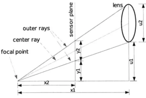
Focal Length
When picking a lens the most important factor is the focal length. When rays of light hit a convex lens, they are focused at some point behind the lens. The distance of the focal point to the lens is directly related to the distance of the light source to the lens and the lens properties. The further away the light source, the closer the focal point to the lens. The closest a focal point can be to the lens is when the light source is infinitely far away and the incoming rays are therefore parallel. The distance of this closest possible focal point is the focal length (Figure 3-2).
The focal length depends on the properties of the lens, such as radius of curvature
focal length
on each side (f the lens and the ind oU 111a'ctinJ11. Te iiimula rlaltig 16 wO
is the lens maker's formula:
11 1
I- =(n - 1
f (R1 R2
where
f
is the focal length, n the index of refraction and R1 and R2 are the radiiof curvature of the two sides of the lens. The focal length therefore combines all the properties of the lens into one variable. This is very convenient and makes picking the right lens easier.
Once the focal length has been determined all other focal points can be calculated.
If a light source is at a distance x, from the lens, then the focal point (xi) of this
source can be found at
1 1 1
Xi
f
X8This is the Gaussian lens formula. If several light sources are placed in front of a lens, at the same distance with different angles, all the focal points of each of the light sources will be at the same distance.
3.2.2
Blurring
The focal length by itself, however, is not information enough to pick a lens. Unfor-tunately our light source (the pen) is moving and therefore the corresponding focal point is moving. An auto-focus function as used in regular cameras could adjust for this. The auto-focus first measures the distance of the object (in this case the light source) and mechanically moves the lens, so that the film is at the focal point distance from lens. For an auto-focus to be useful in our case, the mechanics would have to adjust the lens very fast, at the rate of 1 of a second. An auto-focus this fast does not yet exist. Therefore, we have to use a fixed focal length, meaning the lens does not change distance to the virtual image plane where our sensor is located.
When moving the pen, the focal point will move back and forth through the plane of the image sensor. This means the image of the pen will be blurred when the focal