HAL Id: tel-00002751
https://tel.archives-ouvertes.fr/tel-00002751
Submitted on 18 Apr 2003HAL is a multi-disciplinary open access L’archive ouverte pluridisciplinaire HAL, est
To cite this version:
Susana Trasobares. Synthesis and Characterization of New Carbon Nitrogen Structures, Thin Films and Nanotubes. Physique [physics]. Université Paris Sud - Paris XI, 2001. Français. �tel-00002751�
UNIVERSITE PARIS-SUD
CENTRE D’ORSAY
THESE Presentée pour obtenir
Le GRADE de DOCTEUR en SCIENCES De l’Université PARIS XI ORSAY
par
Susana TRASOBARES LLORENTE
SYNTHESIS AND CHARACTERISATION OF NEW CARBON NITROGEN STRUCTURES: THIN FILMS AND NANOTUBES
Soutenue le 27 septembre 2001 devant la Commission d’examen
P. Berthet Président S. Csillag Rapporteur A. Loiseau Rapporteur C. Colliex B. Jouffrey O.Stéphan D.R.M. Walton Invité
« Aunque estemos separados por miles de kilometros nuestros corazones estaran siempre cerca »
It is extremely difficult to thank in only few lines all the people that have been involved in this thesis. Before starting the acknowledgements, I would like to apologise if I forget any name but I will try to do my best and do not leave any of “you” outsidefrom this list. Also trying to make personalised acknowledgements and after a so European thesis, some changes of language are unavoidable
First, I would like to thank Prof. Christian Colliex for permitting me to be part of the group STEM at Laboratoire de Physiques des Solides (LPS) where the scientific environment is exceptional. The high number of collaborations that this group lead by C. Colliex has, has permitted me to work with people from different countries, to attend a huge number of conference and to meet different cultures which I did not have the chance to know. Also I would like to thank him for the fruitful discussions and for giving me the opportunity of learning something completely new for me: the Transmission Electron Microscopy technique and more particularity the Electron Energy Loss Spectroscopy.
I thank G. Hug for welcoming me to ONERA, Chatillon. I started to work on CNx films and CNx molecules with him. His theoretical knowledge about EELS spectra simulation has constituted a great support in order to interpret our experimental results.
O. Stéphan, apart from being an exceptional person in the professional and friendship aspect., has been one of the mainstays of this thesis. The success of this thesis could be difficulty achieved without her help. She has been patient enough to explain me, one after other, any conceptual aspect, which I did not have before arriving to this microscopy field due to my completely different background. Also many thanks for her availability, the fruitful discussions and her good advice.
I would like to thank Prof. P. Berthet for accepting to be the president of the jury, A. Loiseau for accepting to be one of the examiners and for all her useful comments, which have been essential for improving the manuscript thesis. I would like to thank S. Csillag for accepting to be examiner of my thesis and for spending part of the summer going through the manuscript. I also acknowledge Prof B. Jouffrey for being part of the thesis jury.
British Council-CSIC fellowship. Prof H.W. Kroto and Dr. D.M.R. Walton are thanked for accepting me in their group and for giving me such fruitful time in Sussex. Special thanks are given to Dr. David Walton who has accepted to be member of the thesis jury and has travelled to Paris to attend my thesis. Thanks are given to Dr Kuang W. Hsu for his help with the experiments, the fruitful discussions and his friendship. From Sussex, I also would like to thanks Dr. Malcolm I. Heggie for his continuous support during all these years (muchas gracias Malc de tu siempre amiga). Also many thanks are giving to a person who I met in Sussex and has been really special since the first day, Kostas: thanks for your friendship and our long telephone conversations which helped me a lot in many moments.
I would like to thank A. Kolitsch and S. Malhouitre from Institute Rossendorf, Dresden, G. Safran and G. Radnosky from Hungarian Academy of Science for providing the CNx films samples and for the successful discussions. Thanks are given to Prof. L. Pettersson and C. Kolczewski from FISIKUM at Stockholm University for their important contribution with their theoretical calculations. Prof. J. Zhu and S. P. Gao from the University of Tsingua, Beijing for their successful collaboration in the CNx nanocrystals.
It has been an honour for me to be part of the TMR Network “Synthesis, structure and properties of new carbon based hard materials” co-ordinated by S. Csillag. This network provides an indispensable financial support. Further more it provides a good working and social environment. Working in this network has provided fruitful collaborations and given me the opportunity of knowing excellent people from different places (Stockholm, Linköping, Dresden, Toulouse, Bordeaux, Paris, Newcastle, and Budapest). Thus I would like to thank everybody belonging to this TMR Network. Special thanks to Riitta Raty, who spent one year as a post-doc at LPS. Apart from teaching me the basis about the characterisation techniques, she has made easier my stay in Paris. Thanks Riita for the nice time we have passed together working, sharing the office, discovering France, learning the French culture (French). Also I would like to thank Niclas Borglund (this time it is not in a train station), for his friendship and all nice time we have shared during this three years in the TMR meetings, in Barcelona, in the bars.
advice during acquisition experiments. I would like to thank Mathieu for his continuous support and help on the Akashi experiments. Also thanks for the nice time spent together either in the lab or in any of our travels for conference. I would like to thank Dom who has been my office-mate during the last two years of this thesis and had to stand all my questions, music and so on. I also would like to thank Dario for the Italian coffee breaks during the hard working days. Claudie, Daniele, Lolwa, Nathalie, Abdel (and Therese) and Marc are thanked for their friendship and support.
A pesar de estar lejos de Zaragoza (a unos 1200Km) todos vosotros habeis estado muy cerca de mi y sobre todo me habeis ayudado mucho con vuestro incondicional apoyo. En esta ultima parte de los agradecimientos (pero no la menos importante) me gustaria agradecer a mi familia y amigos.
2 CARBON BASED MATERIALS ...13
2.1 CARBON CRYSTALS ... 15
2 .1.1 DI A MON D ... 15
2 .1.2 GRA PHI T E... 16
2 .1.3 FULLEREN E CRYS T A LS ... 17
2 .1.4 N A N OT UBES ... 18
2.2 BONDING AND ELECTRONIC CONFIGURATION IN THE CARBON CRYSTALS...20
2.3 DOPING C CRYSTALS ...23
2 .3 .1 N -DOPED DI A MON D...2 4 2 .3 .2 N -DOPED GRA PHI T E ...2 5 2 .3 .3 A Z A FULLEREN ES ... 2 6 2.4 CNXCOVALENT SOLIDS...27
2 .4 .1 C3N4 COVA LEN T S OLI DS ...2 8 2 .4 .2 CNx COVA LEN T S OLI DS (x 1) ...3 2 2 .4 .3 CNx N A N OT UBES ... 3 5 2 .4 .4 C-N BON DS ...3 6 2.5 PERSPECTIVES AND PRESENT WORK ...38
3 SYNTHESIS METHODS... 39
3 .2 .1 CHEMI CA L VA POUR DEPOS I T I ON (CVD)... 4 7
3 .2 .2 PYROLI S I S OF ORGA N I C PRECURS ORS ;
S ynt he s is of CNx N anot ub e s ... 4 8 3.2.2.1 PYROLYSIS SET-UP ... 49 3.2.2.2 ORGANIC PRECURSORS... 50 3.2.2.2.1 Melamine (1,3,5 triamino-triazine) ... 52 3.2.2.2.2 Camphor ... 53 3.2.2.3 CATALYST ... 54
3.2.2.3.1 Laser etched films ... 56
3.2.2.3.2 Catalyst as powder ... 60
3.2.2.4 GAS FLOW...61
3.3 SUMMARY AND INTRODUCTION TO NEXT CHAPTER... 62
4 CHARACTERISATION TECHNIQUES...63
4.1 (SCANNING)-TRANSMISSION ELECTRON MICROSCOPE, (S)TEM... 65
4.2 SAMPLE PREPARATION ... 68
4 .2 .1 PLA N E-VI EW S A MPLE ... 6 9 4 .2 .2 CROS S -S ECT I ON S A MPLE ... 7 0 4.3 HRTEM (TEM) AND ADF (STEM) IMAGING ... 70
4 .3 .1 HRT EM I MA GES ... 7 1 4 .3 .2 I MA GI N G W I T H A S T EM ... 7 3 4.4 ELECTRON ENERGY LOSS SPECTROSCOPY ... 79
4 .4 .2 I N FORMA T I ON T O BE EX T RA CT ED FROM
A N EELS S PECT RUM ...8 5
4.4.2.1. LOW ENERGY LOSS REGION ...86
4.4.2.2. CORE LOSS REGION...88
4.4.2.2.1 Identification and Quantification...88
4.4.2.2.2 Near Edge Fine Structures ... 91
4.4.2.2.3 Multivariate Statistical Analysis and Non Linear Square Fiitting (NNLS) analysis...95
5 RESULTS-SUMMARY OF THE PAPERS ... 101
5.1 PAPER I "MODULATED CNXFILMS PREPARED BY ION BEAM ASSISTED DEPOSITION" ...103
5.2 PAPER II, "COMPARTMENTALISED CNXNANOTUBES; CHEMISTRY, MORPHOLOGY AND GROWTH PROCESS" ...105
5.3 PAPER III, "ISOLATING AND IDENTIFYING THE ELNES SIGNAL OF CN NANOCRYSTALS " ...107
5.4 PAPER IV, "A ROUTE TO STUDY THE CARBON-NITROGEN BOND: CHRONO-SPECTROSCOPY IN MELAMINE"... 107
5.5 PAPER V,
6 CONCLUSIONS AND PERSPECTIVES... 111 7 REFERENCES ... 119 PAPER I ... 131 PAPER II ... 153 PAPER III ... 165 PAPER IV ... 183 PAPER V ... 209 PAPER VI ... 217 8. ACRONYMS ... 255
PRESENTATION OF THE SUBJECT
Without materials, there would be no social progress. Materials are daily transformed and used for benefit of mankind. The importance of the materials in our life can be deduced by just looking at how many different materials pass through our hands along one day, polymers, semiconductors, composites in the form of clothes, computers, automobiles etc…
Hard materials are valuable in industry for use in cutting tools, abrasives and wear-resistant protective coatings. Diamond has long been considered as the hardest material in the nature. However a provocative and potentially useful prediction of a new material, carbon nitride, which would rival or exceed the hardness of diamond, came out in 1989. Using a pseudoempirical calculation Liu and Cohen suggested that a compound made of carbon and nitrogen covalently bonded, β-C3N4 which presents similar
structure to that of β-Si3N4, could behave as an ultra-hard material
presenting high thermal conductivity and useful electrical and optical properties [1,2]. If this material exists it could serve as an inexpensive substitute for diamond, or it could be used to carve diamonds into intricate shapes for uses as semiconductors in electronic devices. Moreover super-hard materials could be used to cut steel and thin layers of metal, which can not be done with diamond. Mechanical components such as gear and bearing coating made of super-hard compounds, would last much longer than normal pieces, and could be used in machines where liquid lubricants are unsuitable.
This prediction about the stability of β-C3N4 or other carbon
nitride crystalline structures has motivated researchers to develop different synthesis methods for producing such stimulating compounds.
Only a few experimental studies on CN films show crystallites embedded in amorphous CN films [3-7]. Moreover, the N content observed in the samples is usually lower than that expected for C3N4. Experimentally it has
been shown that films with low N content like CN0.2 films with
fullerene-like microstructure (three-dimensional network of covalent C-N bonds) possess a hardness and an elastic modulus (60, 900 GPa) close to those of
diamond (100, 1050 GPa) [8]. The experimental evidence of hard CNx
materials has motivated further theoretical studies on new CN structures. Miyamoto et al have proposed the existence of CN tubules, which should be metallic independently on their diameter and chirality [9]. Recently, different chemical and physical synthesis routes (as for example chemical vapour deposition (CVD), magnetron sputtering, and electron cyclotron resonance) have achieved the production of CNx nanotubes. The highest
N/C ratio (~0.7) has been found in “amorphous nanotubes” prepared by electron cyclotron resonance [10].
Despite many efforts to produce such exciting materials, characterisation of the sample by diverse techniques has shown that a crystalline material is rarely obtained and when it is present it appears in the form of small crystals embedded in an amorphous matrix. Because of the small size of the crystals and the presence of amorphous matrix, the structure of the produced crystalline carbon nitride is still not completely defined, a mixing of β, α (derived from α-Si3N4), and other phases has been
reported [5,6] and other new structures have been theoretically predicted. Therefore, in order to fully characterise the material, information about the bonding configuration is essential. Using X-ray photoelectron spectroscopy XPS analysis, the first experimental evidence of C-N covalent materials was reported by Niu et al [11]. This technique has also been used
results are still controversial due to the uncertainty in the absolute position of the peaks and the choice of number of peaks used to fit the spectrum. The small size of the crystal structures, the presence of amorphous material and the inhomogeneity of the material make the characterisation of the CNx materials highly difficult. A technique at the
nanometer scale, which will also provide information about the chemical and bonding configuration of the elements, is needed. As it will be further described (chapter 4), Electron Energy Loss Spectroscopy (EELS) in a transmission microscope permits to correlate a spectroscopic information to morphological and structural features of the specimen, allowing an accurate characterisation of materials at the nanometer scale [13,14]. Moreover, the last developments performed in the dedicated Scanning Transmission Electron Microscope (STEM) available in Orsay, have reduced the required acquisition times for achieving a satisfactory signal-to noise ratio on any spectrum up to the order of 1-5 milliseconds for the plasmon region and of 50 milliseconds to 1 second for the core loss region. This short time permits us to investigate the transformation of the materials under the beam (Time Resolved EELS) and increases the area of analysis by performing 1D and 2D scans on the sample (Spatially Resolved EELS).
Nowadays, the observed N/C ratio and the crystallinity in CNx
materials are still far from that of the predicted C3N4. Further work on
production and characterisation of CNx material is needed in order to
understand the N incorporation process in the C network. In this context, the Training Mobility Research (TMR) network “Synthesis, structure and properties of new carbon based hard materials” was created in 1997. Groups belonging to different countries in Europe (France, Sweden, England, and Germany) have collaborated to produce and characterise materials both hard and flexible. As part of this network, this thesis deals with the synthesis and characterisation of CNx materials. Particularly,
Transmission Electron Microscopy (TEM) and Spatial and Time Resolved EELS have been used in order to extract information about the atomic structure and bonding configuration of CNx films and nanotubes as well as
to monitor the CN transformation under the beam.
The CNx films were prepared by our collaborators at Institute
Rossendorf and sent to our laboratory for characterisation. The CNx
nanotubes samples were synthesised in collaboration with Dr W. K. Hsu during my stay at Sussex University, Brighton (1998, and short period of time in 1999).
PLAN OF THE THESIS
In the following chapter, chapter 2, an introduction to carbon based materials and the effect of incorporating nitrogen on the properties of such materials (structural, electronic, optical…) is reported. In chapter 3, the synthesis methods utilised for the preparation of CNx materials are
described. Particularly, the pyrolysis system as well as the effect of the different synthesis parameters in the production of CNx nanotubes are
written up.
In chapter 4, the characterisation techniques (TEM and EELS) are described. Spatially and Time Resolved EELS (acquired methods) and the different processes used for extracting the information from the acquired data (Multivariate statistical analysis, MSA, and Non Negative Least Square fitting (NNLS)) are explained.
Finally, in chapter 5, a summary of the papers presented in this dissertation is given. The first paper "Modulat ed CNx f ilms pr e par e d b y I on
CNx films prepared at Rossendorf Institute, the TEM analysis was carried
out by the group in Budapest and the EELS analysis was performed at the Laboratoire de Physiques des Solides in Orsay. In Paper II, "Compar t me nt alis e d CNx nanot ub e s ; Che mis t r y, Mor phology and Gr owt h
pr oce s s ", the effect of the different synthesis parameters in the incorporation of N into carbon nanotubes produced by catalytic pyrolysis is reported. As a result, a growth mechanism for such structures is proposed and a comparison of the results with those previously reported is also carried out. Paper III shows the identification of the CNx nanocrysrtals
embedded in an amorphous CNx matrix. Papers IV, "A rout e t o st udy t he
Car b on-N it r oge n b ond: Chr ono-s pe ct r os copy in me lamine ", and V "Elect ron Be am Punct ur ing of Car b on N anot ub e Cont aine r s f or Re le as e of S t or e d N2
Gas ", are the results of in-situ EELS experiments. The former describes the decomposition process of melamine under beam radiation as well as the identification of the different decomposition stages by EELS. In the latter a new nanotube morphology, nanotubes containing nanocapsules, is reported. Moreover, using time-resolved analysis, the transformations produced in the carbon nanotubes when a high-energy electron beam is focused on it, are monitored and simultaneously analysed. Finally, paper VI is a review concerning EELS on carbonaceous materials of the different studies performed at the Laboratoire de Physiques des Solides, thus part of the results obtained in CNx materials are included.
2.1 CARBON CRYSTALS
Carbon is present in the nature in various crystalline and amorphous phases. The two best-known allotropic forms of carbon are diamond and graphite. However, a new crystalline form, which is based on a molecule
with 60 C atoms called buckminsterfullerene (C60, fullerene), was
discovered in 1985 by H.W. Kroto et al. [15]. This fascinating result did open up the research field on new carbon nano-structures, leading in 1991 by S. Iijima, to the discovery of another crystalline nano-structure [16], called nanotubes.
2.1.1 DIAMOND
The ideal structure of diamond has the characteristic that every C atom is surrounded by four other C atoms at the corners of a regular tetrahedron with a cube edge length of ao= 3.567Å. This carbon is bonded
to these neighbours by strong covalent bonds (bond length 1.544 Å), Figure2-1A. The close-knit bonded crystal structure yields diamond special properties, which are different from those of graphite or other C forms. Apart from being one of the most expensive gemstones, it has a higher sound velocity than any solid, it is also the best conductor of heat and the hardest naturally occurring substance known. All these special properties provide it with huge number of applications. It is used to produce hard coatings for industrial equipment such as grinding wheels, machine tools and mining drills. Diamond films, grown on various materials by subjecting carbon containing gas to extreme heat, can also be used in windows for
optical devices, or substrates for semiconductors. In addition, industrial diamond, which presents many imperfections and is directly extracted from a mine or synthesised, is used as abrasive.
Figure 2-1.- Structure of diamond A) and graphite B).
2.1.2 GRAPHITE
Graphite, also called plumbago or black lead, has a layered structure that consists of rings of six carbon atoms arranged in widely spaced horizontal sheets. The carbon atoms are arranged in an open honeycomb network, so that the A and B atoms of consecutive layers are on top of one another, but the A' atoms in one plane are over the unoccupied centres of the adjacent layers, Figure 2-1B. This gives rise to an ABAB planar stacking arranged with an plane nearest neighbour distance C-C of 1.421 Å, an in-plane lattice constant ao of 2.462Å and an interplanar distance co/2 of
3.359 Å. Contrary to diamond (isotropic, cubic and insulating crystal),
A)
B)
ao
a1 a
graphite is highly anisotropic, exhibiting metallic behaviour in the basal plane and poor electrical conductivity along the c axis. In terms of mechanical properties it is a soft slippery solid and along with diamond it exhibits the highest thermal conductivity. It is used in lubricants, pencils, foundry facing and because it conducts electricity but does not melt, graphite is also used for electrodes in electric furnace and dry cells as well as for making crucibles in which metals are melted.
2.1.3 FULLERENE CRYSTALS
It is the third form of crystalline carbon known to exist, after the solid network solid of graphite and diamond. By definition, a fullerene molecule is any of a class of closed, hollow, aromatic carbon compounds that are made up of 12 pentagonal and different hexagonal faces. [17]. It consists of an even number of carbon atoms, in a range of from 32 to 600 atoms. The first discovered fullerene was the buckminsterfullerene (C60),
which is made of 60 C atoms located at the vertices of a truncated icosahedron where all carbons sites are equivalent, Figure 2-2A. The C60
molecules, also called bucky-balls due to their spherical molecular shape, are quite strong and almost incompressible. In the solid state, the C60
crystallise into a face centred cubic (fcc) lattice structure, with a one nanometer spacing between the centres of two adjacent balls, which are weakly bonded by Van der Waals interactions. The physical and chemical properties of fullerene crystals are still investigated, however it is known that a C6O solid can resist very high temperatures and pressures without
losing its structure. The outer surface of the molecule is highly reactive and the cavity can be used to encapsulate different atoms. Recently, the
identification of Gd atoms inside fullerenes (Gd@C60) enclosed in a single
nanotube, Figure 2-2B, has been reported [13]. The unique structure and properties of buckminsterfullerenes suggest potential utilities for fullerenes as superconductors, lubricants, industrial catalysis and drug-delivery systems (e.g. target cancer therapy).
Figure 2-2.- A) Fullerene structure B) HRTEM of a single nanotube
containing fullerenes which have Gd atoms encapsulated as indicated in the scheme, the scale bar corresponds to 3nm, (courtesy of K.Suenaga)[13].
2.1.4 NANOTUBES
The structure of carbon nanotubes has been efficiently studied by Transmission Electron Microscopy (TEM) [16] yielding a direct confirmation that nanotubes are cylindrical structures based on the hexagonal lattice of carbon atoms that forms crystalline graphite, Figure 2-3A. Depending on the number of walls present in the nanotube, they can be classified as single wall nanotube (SWNT, only one wall, Figure 2-3B) or multiwall nanotubes, Figure 2-3C, when the nanotube is made of coaxial cylindrical
layers. A single wall nanotube can be understood by a simple construction of rolling a perfect graphite sheet. Thus, three kinds of nanotubes are possible depending on how the graphite sheet is rolled up: "Armchair", if the nanotube axis is perpendicular to one C-C bond, "zigzag" when the nanotube axis is parallel to one C-C bond and "chiral" nanotube in any other intermediate structure. The electronic properties of nanotubes depend on their chirallity and diameter. Consequently controlling their structure
Figure 2-3.- A) Nanotube scheme, HRTEM images of a SWNT B) and C)
MWNT. D) Full colour flat display made of carbon nanotubes.
means also handling their properties. Nanometre-scale devices could therefore be based on coaxial nanotubes or junctions between nanotubes; for example a metallic inner tube surrounded by a large semiconductor (or insulating nanotube) would form a shielded cable at the nanometre-scale
A)
[18]. Because of their very small diameter (from 1 to a few nanometers) and relatively long length (up to several microns), carbon nanotubes are perfect test nanostructures for studying one-dimensional physics, both theoretically and experimentally. For example the Luttinger like liquid behaviour of the electron gas was evidenced by tunneling transport experiments [19,20]. The investigations on transport properties have lead to the discovery of proximity induced superconductivity in SWNT's [21] and intrinsic superconductivity [22]. Moreover, Treacy et al have reported that thanks to their high crystallinity and high aspect ratio nanotubes have an exceptionally high elastic Young's modulus (five times the value for steel) [23] and they could be used in lightweight-bullet proof vest and earthquake resistant buildings. However further progress is still needed in order to optimise the properties of the nanotubes, to create materials by incorporating the nanotubes in a matrix. As first applications, tips for scanning probe microscopes and full colour flat displays made of carbon nanotubes are already available on the market [24].
2.2 BONDING AND ELECTRONIC CONFIGURATION IN THE CARBON CRYSTALS
We have already seen that although the above crystalline phases are made up with the same atomic element, carbon, they present different structures and properties. Carbon is a good metal in the form of graphite, a wide gap semiconductor as diamond or fullerene and superconductor when intercalated with appropriate guest species. Furthermore, carbon-based electronic materials provide examples of materials showing the entire range of dimensionalities from fullerenes which are 0D quantum dots to
carbon nanotubes which are 1D quantum wires, to graphite a 2D layered anisotropic material, and finally to diamond a 3D isotropic solid. The diversity in the properties of the C based materials finds its origin in the differences in bonding configuration.
The valence-shell electron configuration of an isolated carbon atom is 2s2 2px1 2py1 which suggests that it can form only two bonds, in which case
carbon would have a valence of 2. However the normal valence of carbon in its high variety of compounds is 4. When considering bonding with neighbouring atoms, apart from s and p orbitals, hybridised wave functions are formed as a result of a linear combination of the well-oriented orbitals. Thus three kinds of hybridisation are possible in C atoms;
* When one 2s and three 2p orbitals of a carbon atom are hybridised, they give rise to four lobe-like sp3 hybrid orbitals, that are equivalent to one another apart from their orientations, which are towards the four corners of a regular tetrahedron, Figure 2-4A. Each hybrid orbital contains an unpaired electron and can form four σ bonds, bonds in which the electron density has a circular symmetry when viewed along the bond axis.
* The sp2 hybrid orbitals, Figure 2-4B, have lobe-like boundary
surfaces that point to the corners of an equilateral triangle. They are the result of a coupling between one 2s and two 2px-y orbitals
which leave an unhybridised 2pz orbital now side-by-side which can
overlap to form a π bond (presence of delocalised π electrons and double bonds).
* sp hybridisation, Figure 2-4C, is present when one 2s and one 2p orbitals are mixed leaving two 2p unhybridised orbitals ready for forming π bonds (triple bonds). This hybridisation is mainly observed in molecules as acetylene.
Figure 2-4.- A) sp3 B) sp2 and C) sp hybrid orbitals.
The cohesion in compounds or crystals is insured by the formation of
bonds between atoms. Thus diamond is made of pure sp3 carbon atoms
which are strongly covalently bonded, the absence of π electrons makes diamond an insulating solid. In graphite the carbon atoms are truly sp2 bonded with a planar configuration in contrast to the case of fullerenes
where the sp2 bonding between adjacent carbons occurs on a curved
surface. This curvature of the trigonal bonds in C60 leads to some
admixture of sp3 bonding, characteristic of tetrahedrally bonded diamond but absent in graphite. In sp2 bonded networks like graphite and nanotubes, the π electrons are delocalized, and a resonance structure is formed. There is not single or double bonds, instead each carbon-carbon bond can be treated as having a bond with a length in between that of double and single bond. The presence of delocalized electrons makes graphite and nanotubes (for given diameter and chiralities) a good electrical conductor.
2.3 DOPING C CRYSTALS
The electronic properties of the materials can be drastically changed by the presence of impurities. When an impurity is added to a system, a slight modification is observed in the energy bands. From the electronic point of view, two types of impurities can be present, donor and acceptor impurity. In the former one, also called n-type doping, the impurity provides an extra electron, which can only be accommodated in the conduction band (for example N in carbon materials). In the latter, denominated p-type doping, the impurity provides one less electron to the system and therefore leaves one state unoccupied in the valence band (B in C systems). From the chemistry point of view, the impurity, atomic or molecular species, can be incorporated in the crystal structure by substituting a C atom (doped C, typically observed in diamond) or by being intercalated between the C layers (intercalated C in graphite). In the case of diamond, which presents strong sp3 bonding and high isotropic character, the intercalation is not possible. On the other hand, in the case of cages or tubes, because they are closed, the guest-species can also be encapsulated in their cavity.
Since a carbon atom is very small and the average nearest neighbour C-C distance in only 1.41 Å in graphite, it is believed that the only likely substitution dopant in graphite is boron. However few works have already been reported about N-doped graphite, as it will be shown below. Because diamond has a larger neighbour distance C-C=1.54 Å, both boron and nitrogen can enter in the diamond lattice substitutionally. In the case of fullerenes the C-C distance is slightly larger than that in graphite and the
surface. Consequently it may also be possible to dope the C60 shell with N
atoms.
2.3.1 N-DOPED DIAMOND
In the case of diamond, impurities play a very important role because they induce changes in the electrical and optical properties. The best nature diamond contains impurities with concentration in the range of 1 part in 105. However only few species can enter in the diamond structure (B, N) and when doping is possible, the concentration is very low. It has been observed that the strong infrared absorption of Ia diamond (specific kind of diamond [25]) is due to the fairly amount of N (up to 0.1%) inhomogeneously distributed in the crystal and mainly concentrated in small agglomerates. Besides, because of their negative electron affinity, diamond surfaces terminated with hydrogen are expected to emit electrons spontaneously and therefore they could be used in microelectronics and flat-panel displays. However in order to use diamond in battery-driven cold cathodes a low-threshold emission is needed. Okano et al [26] have measured the electron emission of diamond surface doped with nitrogen Figure 2-5. Comparing the results with those obtained in samples doped with boron and phospohorous, they observed that the difference in the emission properties are fundamentally due to the different impurities induced in diamond and the lowest threshold field is present in the N-doped diamond. Nevertheless it is still not clear which is the real effect of N in the diamond system. Recently, Show et al [27], studying the electron emission from nitrogen doped diamond films (N/C from 0 to 10), reported that the N atoms are located at a substitutional site, providing paramagnetic defects in the diamond film and increasing the current density of the electron emission.
Figure 2-5- A) Schematic structure of the electron emission measurement circuit, inset morphology of the diamond surface doped with nitrogen. B) Comparison of emission properties of N, B and P doped crystalline diamond films (courtesy of K. Okano) [26].
2.3.2 N-DOPED GRAPHITE
Because of the weak van der Waals forces between the graphite planes, two kind of modifications of graphite can occur. Apart from reactions occurring at defect sites or domain boundaries, graphite can be intercalated both by donor and acceptor species. Up to now there is not much done on N-doped graphite. Few attempts to incorporate nitrogen in graphite by thermal decomposition of hetereoaromatic compounds [28] have shown that disorder graphite domains with a N enrichment in their periphery are formed. Moreover N is easily eliminated when the sample is
exposed at temperature. Using a non-equilibrium doping exposure of the graphitic domains to hot N atoms, N-doped graphite has been produced and its structural and electronic properties have been determined [29]. When graphite is doped with N (N incorporated =2.3%), the graphitic lattice is expanded, the gap is narrowed and the conductivity increases. Dos Santos et al, using semiempirical pseudopotential techniques, have found a transition from planar to corrugated structures upon nitrogen incorporation for concentrations above 20%. Buckling of the structure leads to localisation of electrons in the lone-pair orbitals [30].
2.3.3 AZAFULLERENES
Each carbon atom in a C60 is in an identical environment. Since all the
intramolecular bonding requirements of the carbon atoms are satisfied, it is expected that C60 is a van der Waals insulator (semiconductor) with an
energy gap between the occupied and unoccupied states in agreement with optical measurements [31]. To make C60 conducting, doping is necessary to
provide the charge transfer and to move the Fermi Level into the conduction bands. Because of their structure, fullerenes can be doped in several different ways. Endohedral doping, where the dopant is located in the hollow core of the fullerene, exohedral doping where the dopant is outside or between fullerenes and finally substitutional doping (also called "on-ball") where the dopant substitutes one or more of the carbon. The chemistry of heterofullerenes only opened in 1995 when C59N and its dimer
(C59N)2 were isolated for the first time [32]. However earlier studies had
shown the strong interaction between nitrogen and C60 in CnNm molecules
hetereofullerene is almost identical to the parent neutral material, which could be of essential importance in separation of liquid fractions of hetereofullerenes [34]. From quantum chemical calculations, optical absorption spectroscopy and electron energy loss spectroscopy it was found that (C59N)2 is non-metallic and has an optical gap of 1.4ev, 0.4 eV
smaller than that of solid C60 [35]. Recently Stäfström et al, using ab initio
quantum chemistry type of calculations, have studied the stability of a series of azafullerenes C60-2nN2n. [36].
2.4 CNx COVALENT SOLIDS
Apart from modifying the electronic properties, the presence of hetero-atoms in C based compounds, could influence the mechanical properties. Hardness is a quality related to the extent to which solids resist both elastic and plastic deformations. On the microscopic level (for ideal systems) hardness is determined by the bulk modulus (B), which can be defined in tetrahedral solids using the Philip van Vechtem scheme [1] as following:
B = 19.71−2.20 d3.5 (1)
where B is the Bulk modulus in megabars, d is the bond length in angstrom and λ is an empirical term which takes into account the ionic contribution to the bond. Using the above model, Liu and Cohen predicted the stability of the β-C3N4. Moreover, Sjöström et al have experimentally observed that
CN0.2 films with fullerene-like microstructure (three-dimensional network
of covalent C-N bonds), have hardness and elastic modulus (60, 900 GPa) close to those of diamond (100, 1050 GPa) [8]. Therefore it is expected that incorporation of N in C based materials provides a new class of materials with exciting electrical and mechanical properties.
2.4.1 C3N4 COVALENT SOLIDS
The crystalline β-C3N4, which structure is based on the known
β-Si3N4 where C substitutes to Si, has been predicted to be an ultra-hard
material. The structure is shown to consist of buckled layers. The unit cell is hexagonal and contains two formula units (14 atoms) per unit cell with local order such that C atoms occupy slightly distorted tetrahedral sites, while N atoms sit in nearly planar triply co-ordinated sites. This atomic coordination suggests sp3 hybrids on the C atoms and sp2 hybrids on the N atoms. The average C-N distance is 1.47Å intermediate between the C tetrahedrally bonded (sp3) with the sp2 N and C-N sp3 tetrahedral bonded. In 1993 Niu et al claimed the production of a covalent C-N solid by pulsed laser ablation of graphite targets within an intense atomic nitrogen source [37]. Photoelectron spectroscopy showed that the cohesion of the produced solid results from an unpolarised covalent bonding and qualitative tests also indicated that the material is thermally robust and hard. Later on, using different techniques (rf diode sputtering and arc-plasma) Yu et al and Yen et al have reported the production of small crystalline grains (<1µm) [7,38]. From Transmission Electron Diffraction (TED) and Raman characterisation, they claimed that the small grains could correspond to the predicted β-C3N4. , However the obtained N content in the above
Figure 2-6.- Structure of β-C3N4 –blue C and grey N) (Courtesy of M.
Matessini [39]).
Because only microscopic amounts of β-C3N4 are claimed to be
obtained, the study of the mechanical properties can not be performed experimentally. Theoretical calculations have predicted a direct and indirect band gap (6.4 and 6.75 eV respectively) larger than the minimum gap in diamond. Therefore it is suggested that β-C3N4 may find many uses
as a transparent hard material [2]. In addition the velocity of sound in β-C3N4 is estimated to be over 20% larger than that of β-Si3N4. This high
sound velocity could lead to useful thermal properties in β-C3N4, such as
high thermal conductivity [40]. Experimentally further work is needed for confirming the existence of the predicted ultra-hard carbon nitride covalent solid.
In 1995, research activity on CNx materials explode after Sjöström
et al synthesised super-hard and elastic CN0.2 films [8] by reactive dc
magnetron sputtering. From their theoretical and experimental results based on XPS and TEM studies of the CN0.2 sample, they proposed a new
carbon nitride phase, a fullerene-like microstructure. The structure can be
described as graphite-like with interplanar distance of 0.347, 0.209 and 0.120 nm, where the basal planes are curved into a three-dimensional structure due to the presence of pentagons in the hexagonal network. The incorporation of N atoms induces buckling of the basal planes and thereby facilitates cross-linking between the planes by sp3-hybridised carbon, Figure 2-7.
Figure 2-7.- A) Model of fullerene-like microstructure and B) HRTEM
image of a super-hard CN0.2 sample produced by magnetron
sputtering, (Courtesy N. Hellgren)[67].
The above modelling and experimental results have opened up the research in new CN materials with low ionicity and short bond length. In 1996 Teter et al proposed the -C3N4 and graphitic C3N4 structures as new carbon nitride phases, which are energetically preferred over -C3N4 [41]. The α-C3N4 has hexagonal symmetry and contains 28 atoms per unit cell. It can be
described as an ABAB… stacking sequence of layers of β-C3N4 (A) and its
mirror image (B), Figure 2-8B. The graphitic form (g-C3N4) is represented
also been proposed [42] Figure 2-8A. Two different graphitic structures (hexagonal and orthorhombic) have been proposed. In both of them, each carbon atom is three-fold co-ordinated as is one of the four N atoms per cell while the other N are two-fold. A difference in the vacancy ordering is observed between the structures, the N atom between the rings participates in to the π delocalization in the C3N3 heterocycle [43] and
offers the possibility of providing a delocalized electron along the graphitic layer. Mattesini et al have shown that these two graphitic structures have approximately similar energy, however a higher metallic behaviour is expected in the orthorhombic g-C3N4 [39]. Recently, the production of
graphitic C3N4 by thermal decomposition of melamine in the presence of a
nitriding solvent (NH2NH2) has been reported [44]. Cubic and pseudocubic
structures were also proposed by Teter [45]. The pseudocubic-C3N4, Figure 2-8D, can be classified as a defect-zincblended structure type [46]. Each C atom has four N neighbours and each N atom has three neighbours as in the β-C3N4 structure. However the C-N-C angle is close to the sp3
angle (109.47°) rather than to the sp2 value of 120°C. The cubic structure, Figure 2-8C, is based on the high-pressure willemite II structure of Zn2SiO4 where C substitutes Zn and Si, and N substitutes oxygen. The
same year, Wang et al claimed the preparation of a solid, which consists of irregular-oriented prismatic crystals, made of a mixed phase of α, β and tetragonal C3N4, proposing a new tetragonal structure [47].
Despite many efforts to synthesise the C3N4 crystalline structures, only
the production of small crystals in amorphous matrix has been obtained. Moreover the nitrogen content found in the samples is lower than the expected one in the predicted C3N4. Therefore the inhomogeneity of the
sample, the small size of the crystals and the lower N content make impossible the characterisation of the mechanical properties. Consequently, theoreticians have been motivated to search new CNx (x< 1) structures,
which will have closer composition to that founded by the experimentalists, and to prognosticate the mechanical and electrical properties of such new CNx structures.
2.4.2 CNx COVALENT SOLIDS (x 1)
The experimental observation of hard and elastic carbon nitride materials with lower N content than the expected one for C3N4 [8] and the
observation of a transition between graphitic and fullerene like structure [48] has motivated theoreticians to explore crystalline structures with low nitrogen content like C11N4 and CN. A graphitic C11N4 structure with
arranged layers in the stacking sequence AA... has been proposed by Snis et al [49]. In such structure, the nitrogen atoms are two and three-fold coordinated and C atoms are linked to different N. Recently, the stability of this structure has been compared with that found in a three-dimensional structure (α-C11N4) and C3N4, Figure 2-9, showing that C11N4 is more stable
than C3N4. Moreover, the theoretical thermodynamic stability
investigations suggest that the proposed C11N4 phases can be
experimentally produced but they should be probably mixed due to the small energy separation between both structures (0.03eV) [50].
Guo et al have claimed the production of crystalline CN films composed of three mixed phases, two known-phases (α and β) and one unknown phase, which they described as a monoclinic phase[51]. Recently this phase has been theoretically identified as the tetragonal rocksalt phase and a new series of carbon nitride phases having CN stoichiometry, have been predicted by Kim et al [52].
Figure 2-8.- A) Hexagonal structure and stacking order of graphitic C3N4
(gr-C3N4) B) Structure of α-C3N4, cubic (C) and pseudocubic C3N4
D). g-C3N4 -C3N4 c-C3N4 pseudocubic-C3N4 B) C) D)
Using ab initio calculations, the stability of C3N phases has been
reported. It has been shown that different structures, dimerised, polymerised and N substituted graphite, present similar stabilisation energies. Consequently, entropy effects may become important and a wide variety of local structures could be encountered. Furthermore, the calculation of energy barriers between them leads to relatively small values. Consequently at room temperature, C3N compounds may transform dynamically from one structure to another over a limited period of time ( <~ 1 s) [53].
Figure 2-9.- Free-energy (eV/atom) versus atomic volume (Å3/atom) for
various C3N4 and C11N4 (Courtesy of M. Matessini [50])
Atomic volume 3 4 5 6 7 8 9 10 -6 -7 -8 -9 -10 Free Energy g-C11N4 g-C3N4 b-C11N4 psc-C11N4 a-C11N4
2.4.3 CNx NANOTUBES
The exciting properties of nanotubes, the prediction of ultra-hard materials made of carbon and nitrogen and the experimental evidence of B-doping of nanotubes [54] have motivated Miyamoto et al to study the
stability of CNx nanotubes [9]. Using pseudopotential total-energy
calculations, they proposed that C3N4 and CN tubules should be metallic
independently on the tubule diameter and chirality. Following these theoretical calculations, experimentalists have investigated and
successfully achieved different synthesis routes for producing CNx
nanotubes. Sen et al [55] prepared CNx nanotubes (x=0.03-0.09) by
pyrolysis of pyridine using Co as a catalyst. From the current Intensity versus applied Voltage (I-V) curves obtained by scanning tunnelling microscopy (STM) they have observed that the conductance of the C-N MWNT’s (1.2 nA/V) is generally higher than that of multi-wall C nanotubes (0.5nA/V). The production of aligned CNx nanotubes (x ≤ 0.02) by pyrolysis
of triazine over laser-patterned catalytic has been reported by Terrones et al. [56]. The same research group [57] has shown that higher N content (x ≤ 0.07) is observed in the nanotubes when a nitrogen rich organic precursor is pyrolysed. CNx nanotubulites with a homogeneous N content
(x=0.3-0.4) have been produced by magnetron sputtering [58]. However, chemical vapour deposition of Ni-phthalocyanine [59] has provided CNx
nanotubes with inhomogeneous N content (x ≤0.05 in the graphitic region and approximately 0.15 in the amorphous region). Up to now the higher N content has been observed in the amorphous carbon nitride nanotubes produced by electron cyclotron resonance (N/C≈0.72) [60]. However such N content is far away from the C3N4 composition and crystallinity
also shown the difficulty of incorporating a high amount of N in the nanotube.
2.4.4 C-N BONDS
Despite many different structures have been proposed for CNx
material, a well-defined structure is highly difficult to be experimentally obtained. A review about the different chemical structures of N in CNx
seems unavoidable to well-understand such kind of materials.
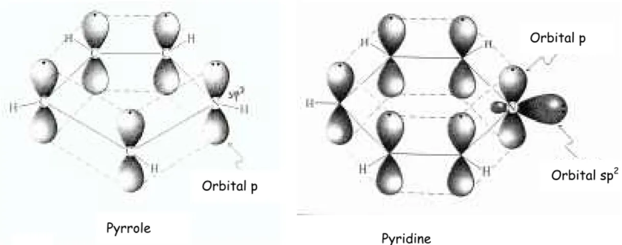
In the case of well-known CNx aromatic systems as pyrrole and
pyridine, the N atoms present sp2 hibridisation but they contribute differently to the molecular orbital structure. The fifth valence electron of the N atom can form a lone pair either with the remaining unhybridized 2pz orbital, or with one of the sp2 orbitals. The first case leads to a
localized 2pz lone pair and the three sp2 hybrid orbitals bond to other
atoms. This case is observed in the pyrrole molecule, fig 2-10A. If the fifth electron instead forms a lone pair with one of the sp2 hybrid orbitals, the atom is left with two sp2 hybrid orbitals and one unfilled 2pz, and can
therefore form one π and two σ bonds as observed in the pyridine molecule, fig 2-10B.
In the case of CNx alloys, the situation is more complex. Using
theoretical models and ab initio Hartree-Fock wave function Casanovas et al [61] investigated the N 1s core level binding energies of N containing carbonaceous materials. They reported the existence of three different C-N bonds, which are associated at different energy binding values.
* Pyridine-like (398eV) refers to N atoms, which contribute to the π system with one p-electron, as in the case of pyridine, fig.
2-* Pyrrolic (399eV) corresponds to N atoms with two p-electrons on the π system, although not necessary in a five-member ring as in pyrrole, fig 2-10B.
* Graphitic like (401-403eV) where N substitutes C in the graphene layers
Shimoyama et al [62], using x-ray absorption fine structure, have confirmed the experimental existence of three different C-N bonds. The existence of pyridine like and graphite like are clearly observed; however the existence of pyrrolic like is not considered, instead the existence of triple C-N bonds is proposed.
Figure 2-10.- Molecular orbitals scheme of two well-known aromatic
systems as pyrrole A) and pyridine B). Orbital p
Orbital p
Orbital sp2
Pyrrole
2.5 PERSPECTIVES AND PRESENT WORK
As it has been above reported, nitrogen plays an important role in the formation of exciting materials like CNx. Its incorporation into graphite
increases the conductivity of the solid carbon, the optical and emitting properties of diamond is improved by adding the optimum amount of nitrogen in the system and CNx nanotubes have been found to have higher
conductance than that found in C MWNT’s. Moreover super-hard elastic
CN0.2 films have been experimentally manufactured by magnetron
sputtering. However there is still much work to do in order to understand the N incorporation process as well as the different possible structures. Different synthesis methods can be used to prepare CNx materials (film
and nanotubes), as it is reported in the next chapter. We will see that most of them lead to the production of amorphous materials.
The first synthesis of CN materials dates from the 70's when Cuono et al prepared paracyanogen-like films by sputtering a carbon target in N2
[63]. Later on in 1982 Jones and Stewart incorporated nitrogen into α-C:H
films by plasma decomposition of methane and N2 [64] . However the
research on CN did not take off before 1989, when Cohen et al proposed that CN covalent solids could behave as ultra hard materials. Such prediction on C3N4 joined to the feasibility of modifying the properties of
C based materials (graphite, diamond, nanotubes) by doping them with N, has increased the number of synthesis routes to attempt the production of such exciting materials. More than ten different synthesis methods have been tested during the last ten years as it is fully reported by S. Muhl and J.M. Mendéz [65]. In this chapter, a summary review of the different synthesis processes used in the production of CNx as well as a detailed
presentation of the synthesis methods used during this thesis (Ion beam assisted deposition and pyrolysis of organic precursors), will be described.
3.1 PHYSICAL METHODS
3.1.1 MAGNETRON SPUTTERING
This technique has been successfully used for the preparation of CNx
and carbon films due to its capabilities of evaporating high melting point materials like carbon, with relatively high flux. A magnetron (Figure 3-1A) consists of a plate of the material of which the film is to be made (carbon target), with magnets arranged behind it to create a magnetic trap for charged particles, such as N ions, in front of the target. When the special magnetron driven power supplier is turned on, the target is subjected to a
voltage, which attracts the ionised gas particles to the target surface at high speed. When the ionised gas particles hit the surface two important effects are produced. i) Atoms are knocked out of the target surface by ions (sputtering). These sputtered atoms are not charged either positively or negatively, so they go straight out of the magnetic trap and they are posteriorily deposited on the substrate to form the coating. ii) The surface also releases electrons, which are negatively. These are hold in the magnetic trap, and their energy is used to produce more ionised gas particles. Therefore the ions which are attracted to the surface are replenished all the time, so that the magnetron can operate continuously. Using this technique, different CNx morphologies have been reported as
CNx films, CNx nanotubulites and CNx nanocrystals in an amorphous matrix
[48,58,66].
Figure 3-1.- A) Magnetron sputtering system B) Diagram phase of the
The first experimental evidence of CN0.2 super-hard elastic films
with fullerene like microstructure was obtained using reactive direct current (dc) magnetron sputtering of a graphite target in pure nitrogen discharges [68]. Moreover a detailed study of the different parameters (ion flux, temperature substrate and nitrogen content) provided a well-defined diagram where the different possible morphologies are related to their concentration of nitrogen and a phase transition between graphitic and fullerene like structures is observed at approximately (5-10% N content), Figure 3-1B. The same group has also prepared carbon nitride nanotubulites (10-50nm in diameter and 20-50 nm in length), which grow perpendicular to the CNx film and are homogeneously made of carbon and
nitrogen [58].
CNx crystals in an amorphous matrix have been grown on
single-crystal Si(100) substrate by reactive sputtering in a radio frequency (rf) magnetron sputtering system. The Si substrate was first etched in 5% HF solution to eliminate the native oxide layer and then cleaned ultrasonically before introduction in the vacuum chamber. The target composed of a C disc, 50mm in diameter, was set 35 mm from the substrate holder. Before
deposition, the vacuum chamber was evacuated to 3x10⁻⁵ Pa and N2
introduced at a constant pressure of 10 Pa. The sputtering powder and the substrate temperature were 175W and 1073K respectively. This sample was prepared in Beijing [66] and sent to our lab where we have performed the characterisation analysis, which will be described later on in this work (paper III).
3.1.2 ION BEAM ASSISTED DEPOSITION (IBAD)
Ion Beam Assisted Deposition (IBAD) is a deposition technique, which combines physical vapour deposition (PVD) with an energetic ion
irradiation from an ion source. The use of an ion source (nitrogen) and of a vapour source (evaporated C on silicon wafers), allows a well controllable, reproducible and flexible IBAD process. Ion flux, atom flux, ion energy, ion incidence angle, arrival ratio of the ions to atoms and the substrate temperature vary independently from each other over a wide range. The deposition can be made by a carbon ion beam in a nitrogen atmosphere (single beam) or by fast-switched carbon and nitrogen sources (dual beam). Most of the as-deposited films are found to be amorphous [69], however Wang et al have recently reported the formation of cubic-nanoparticles
(10-60nm) embedded in the amorphous CNx matrix in a CNx/TiNx
multilayered sample [6] using IBAD.
The CNx films studied during this thesis were prepared by our
collaborators in Rossendorf Institute (Dresden) as following, Figure 3-2A. The Si substrates were mounted on a heater placed at an angle of 45° to the carbon source and normal to the ion beam provided by a 3 inch diameter Kaufman ion source. The substrate temperature could be adjusted between room temperature and 700°C by resistive heating. The base pressure of the chamber was 0.3 Pa and the working pressure was 20 Pa. Prior to deposition, the Si substrates were cleaned in situ by exposing them to an Ar+ ion beam of 1000 eV and a current density of 100 µA/cm2 for 2 min. Carbon was evaporated from a graphite ingot by means of an electron gun (AP&T, HVP4). The evaporation rate of carbon (1-3 Å/s) was measured by a quartz thickness monitor and regulated by an automatic deposition controller. The carbon deposition onto the Si substrate was assisted by a simultaneous nitrogen ion beam. The energy of the N2+ ions
could be varied from 200 eV to 1200 eV. The current density, measured with a Faraday cup positioned on the shutter in front of the substrate holder, could reach 200 µA/cm2. Modulated CN
with the following deposition parameters: ion current density of 40 µA/cm2
and ion energy of 200 eV and the carbon evaporation rate was adjusted to first 0.1nm/s (region A) then 0.2nm/s (region B) and finally again 0.1nm/s (region C). After production the samples were prepared for plane view and cross-section microscopy analysis as it is indicated in section 4.2 (sample preparation for microscopy analysis) chapter 4.
Figure 3-2.- A) Ion Beam assisted deposition system available in
Rossendorf institute for the production of CNx films. B) Bright
Field (BF) image of a modulated CNx cross section sample prepared
by IBAD. electron gun water cooled crucible Nitrogen, argon electron beam Substrate heater Si substrate ionbeam Kaufman Ion source shutter vapour thickness monitor ion beam monitor
C
pump
20 nm A)
3.2 CHEMICAL METHODS
Synthesis of carbon nitride compounds has been attempted by a variety of chemical reactions. A graphite-like hexagonal polymer [(C3N3)2
(NH)3]n has been prepared and found to be stable up to 500°C [70].
Interesting ferromagnetic crystalline material, C3N4O1.2H4.1 have been
obtained from the reaction of C3N3Cl3 and Li3N in N2 at 220°C [71]. Shock
wave compression, a method used in the production of hard materials like diamond and wurtzite boron nitride, has been attempted to produce carbon nitride. Notwithstanding that different carbon nitride organic precursors have been tried, no one has produced hard carbon nitride, however an extraordinarily well-ordered shock synthesis diamond was produced [72]. Nitrogen rich carbon nitride networks (C3N4 and C3N5) have recently been
produced by retarding the decomposition of the energetic molecular azide (C3N3)(N3)3. These compounds are robust and sublime to a significant
extent above 600°C. On the basis of experimental evidence, they can be described as disordered planar system somewhere between cross-linked polymers and graphitic sheets [73].
Other additional chemical processes for CNx production are vapour
growth processes such as chemical vapour deposition and pyrolysis of organic precursors. The former has successfully been used in the
preparation of CNx nanotubes and some groups have also claimed the
production of crystalline C3N4 using such process. The latter did produce
amorphous CNx films, however it has been efficiently used for the
3.2.1 CHEMICAL VAPOUR DEPOSITION (CVD).
CVD provides the formation of a film on a surface from a volatile precursor (vapour or gas), as a consequence of one or more chemical reactions, which change the state of the precursor. Many different films can be deposited with crystalline, polycrystalline, and amorphous structure. Most films can be deposited from several different precursor systems. Plasma discharges can be used to help things along, or the substrate and/or the gas can be heated or cooled.
This technique includes different process direct-current (DC) arc, hot-filament chemical vapour deposition (HFCVD) and plasma enhanced chemical vapour deposition (PECVD). Nevertheless, in every case, CVD processes must: i) provide a volatile precursor containing the constituents of the film, ii) transport that precursor to the deposition surface, iii) encourage or avoid reactions in the gas phase, iv) encourage surface reactions that form the film, v) and do it rapidly, reproducibly, and uniformly for industrial applications.
CVD is one of the most successful techniques for growing CNx films
containing C3N4 crystals. Small grains (~0.1µm) ad nanocrystallites have
been grown and claimed to be β-C3N4 embedded in CNx films [7]. Later on
Veprek et al [74] showed that compact uniform films with the composition C3N4 can be produced by plasma CVD in an intense nitrogen discharge, but
the film was absent of any crystal structure. Wang et al reported the production of pure crystalline C-N films on silicon and nickel substrates by HFCVD. The films were claimed to be constituted of α, β and other unknown phases [5,75].
Recently this technique has also been used for the production of CNx
along the axis and they grow perpendicular to the quartz substrate. EELS on such nanotubes reveal an inhomogeneous distribution of N in the nanotubes. They are nitrogen rich in a few external layers, amorphous in the core of the tube while a slight incorporation of nitrogen is found in the graphite layer. In this dissertation the results obtained by CVD are compared with our results from pyrolysis of organic precursors.
3.2.2 PYROLISIS OF ORGANIC PRECURSORS; Synthesis of CNx
Nanotubes
The pyrolysis of different organic precursors, melamine, triazole, tetracyanoethylene to name a few examples, has shown that the presence of hydrogen in the organic precursor reduces the amount of residual solid due to the thermodynamically stability of NH3, HCN, CH4, which are
released as soon as they are formed. The produced solids are amorphous with a short-range layered structure containing both trigonal carbon and nitrogen [76]. The production of C3N4 thin films by pyrolysis have been
reported by Koubetakis et al [77], the sample results amorphous and the presence of sp2 bonds for carbon and nitrogen is obtained from Infra Red (IR), EELS and Nuclear Magnetic Resonance (13CNMR). Therefore, up to
now the pyrolysis method has not successfully been used for the preparation of CNx crystalline films. However when a catalyst is present,
fruitful production of carbon nanotubes containing nitrogen is achieved. Since the discovering of carbon nanotubes, different synthesis routes have been developed for their production; Arc-discharge and laser evaporation have been found to be well-suited techniques for the formation of large quantities of single and multiwalled nanotubes. However a system
which could work in continuously is needed to scale up nanotube production. Catalytic pyrolysis of organic precursors (vapour growth process) has been found to be a versatile synthesis method because of the possibility of having a continuous process and a better control in the synthesis process than with arc discharge or laser ablation. Moreover, a variety of nanotubes can be produced by only changing the organic precursor and the physical form of the catalyst. The first experimental write up about CNx nanotubes
appeared in 1997 when Terrones et al [56] reported the preparation of aligned nanotubes by catalytic pyrolysis of triazine. The produced nanotubes are highly graphitic and some traces of N (<2-5%) are also detected. One year later, Sen et al [55] produced BCN, CN and BN nanotubes by pyrolysis of precursor molecules over Co catalyst. The quantification of the sample using XPS and EELS indicates a N content of approximately 4%. Although large efforts have been done to produce CNx
nanotubes, only a minor amount of N has been incorporated in the system. Moreover information about how N is incorporated in the system is still lacking. During this thesis, in order to study the dependence of the different pyrolysis parameters on the N incorporation into C nanotubes, series of nanotubes samples, varying the synthesis conditions, were produced.
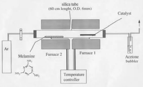
3.2.2.1 PYROLYSIS SET-UP
In the present work, CNx nanotubes and C nanotubes containing
nitrogen were produced by catalytic pyrolysis of an organic precursor. The pyrolysis was carried out in a two-stage furnace system fitted with an independent temperature controller Figure 3-3. The organic precursor 0.10-0.15 g was placed in one end quartz tube (0.6 cm ID, length 60 cm), and the catalyst in a quartz boat at the other end. The tube was located
inside the furnace and subject to a gas flow (20-60 cm3/min). The furnace containing the metal catalyst was heated to temperature of reaction (T) and maintained at this temperature throughout the experiment. Subsequently, the furnace 2, containing the organic precursor, was raised to 950 °C, when it reached the sublimation temperature of the organic precursor, a white smoke appeared inside the reaction tube until the carbon source had disappeared. The furnace 2 was switched off and the furnace 1 was held at the reaction temperature for an additional 15 minutes. After the experiment the obtained black powder was dispersed in acetone for posterior microscopy analysis.
In order to study the dependence of the synthesis parameter (organic precursor, catalyst, temperature and gas flow) on the N incorporation into the carbon nanotubes, a series of experiment, Table 3-1, were performed. First, an organic precursor rich in nitrogen was catalytically pyrolised in an inert atmosphere at different temperatures to control the high yield on CNx nanotubes. The experiments were repeated
using different catalysts to study their effect on the production of CNx
nanotubes. Secondly, N rich gases (N2 and NH3) were introduced in the
system to study the possible increase of N in the carbon nanotubes by increasing the nitrogen source. Finally an organic precursor free of nitrogen (camphor) was pyrolysed in the presence of N rich gases. The results of the above experiments will be described in chapter 5 and papers II and V.
3.2.2.2 ORGANIC PRECURSORS
Using hydrocarbons (benzene, acetylene), carbon nanotubes, graphitic cones and helix-shape graphite nanotubes have been produced
nanotubes with inhomogeneous composition and more recently, CN precursors (as pyridine and triazine) have been used to produce CN nanotubes with N content lower than 3%. During this thesis, melamine (a rich organic precursor) and camphor (a free nitrogen precursor) have been used to produce CN nanotubes and C nanotubes containing encapsulated-nitrogen gas.
Figure 3-3.- Pyrolysis set-up used during the present thesis for producing
Table 3-1.- Series of experiments performed for the dependence study of the N incorporation into the C nanotubes.
Organic precursor Catalyst Gas flow Temperature
Laser etched films Ar 950°C
Ar 950, 850, 750, 550°C N2 950°C N Rich (melamine) As powder (Ni or Fe) NH3 950°C N2 950°C NH3 950°C Free of N (camphor) Fe powder N2/NH3 950°C 3.2.2.2.1 Melamine (1,3,5 triamino-triazine)
Melamine (C3H9N6), Figure 3-6A, also called cyanuramide, or
triaminotriazine, is a crystalline substance belonging to the family of heterocyclic organic compounds. Melamine is manufactured by heating dicyandiamide under pressure. Its most important reaction is that with formaldehyde, it produces resinous compounds of high molecular weight. These resins form under the influence of heat but, once formed, are insoluble and infusible. Usually impregnated with fillers and pigments, they are molded into dishes, containers, utensils and handles or used as laminating agents or coating materials for wood, paper, and textiles. Formica and Melmac are well-known trade names for products based on melamine resins. Melamine has been also used in the production of flame retards [81]. The presence of mobile hydrogen atoms from the amino group, which can be shifted to the N atoms of the aromatic ring, enhances the decomposition process. Melamine, serving as spumific compound, has
ever-increasing importance in plastics industry as flame and heat retardant. Upon decomposition of the spumific compounds, large quantities of non-flammable gases (e.g. N2) are produced. The sublimation temperature of
this compound is approximately 340°C. In the present thesis, melamine (Aldrich 99.9% purity) has been used as C and N source in the formation of CNx nanotubes.
3.2.2.2.2 Camphor
Camphor, (C10H16O), which belongs to a group of organic compounds
defined as terpenoid ketones, has been used for many centuries as a component of incense and as a medicinal. Modern uses of camphor have been as a plasticier for cellulose nitrate and as an insect repellent, particularly for moths. The pure compound is a white, waxy solid that melts at about 178°–179°C.
A) B)
Figure 3-4.- Structure of the different organic precursor catalytic
pyrolised for the production of nanotubes A) melamine (N atoms in blue and C atoms in grey) and B) camphor.
Camphor is derived from Cinnamomum camphora, the camphor tree, of China, Taiwan, and Japan. It is obtained by steam distillation of wood chips. The wood of the camphor tree may contain up to 5 percent of the crude oil, and a single tree can yield up to three tons of the oil, which settles from the distillate and crystallises. Since the early 1930s camphor has been made by several processes from the compound α−pinene. The structure and the peculiar reactions were important problems of 19th-century organic chemistry. At least 30 structures were proposed before the definition of the correct one Figure 3-6B.
During the present thesis, camphor (Technical grade camphor, purity c.a. 98%, Camphor & Allied Products Ltd., India) has been pyrolysed in the presence of nitrogen rich gases and nanotubes containing nanocapsules have been produced, as it will be described in the following sections.
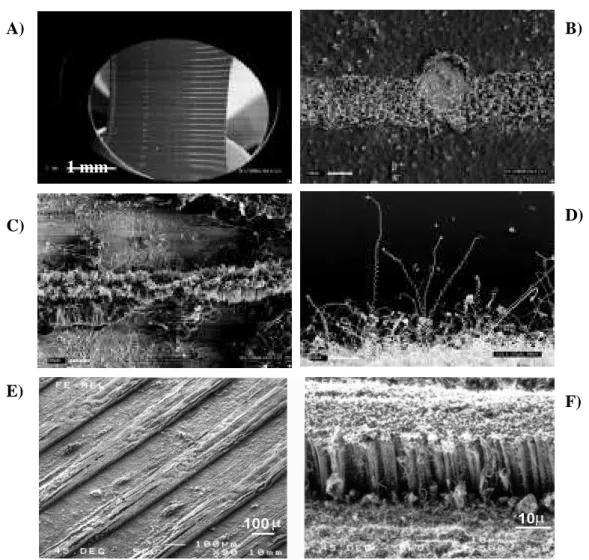
3.2.2.3 CATALYST
The catalyst plays an important role in the production of nanotubes as responsible for their growth. MWNT’s could be produced without any catalyst by arc discharge but their presence is indispensable for the formation of SWNT and when they (MWNT and SWNT) are synthesised by vapour growth techniques like pyrolysis. Despite the importance of catalyst in the growth mechanism, its role or the way that it influences on the nanotubes production is still not clear. Two main growth mechanisms have been proposed; the first one consists of surface diffusion of the carbon species over the catalytic particles ([82], Fig.3-5A). In the second one, the carbon dissolves in the metal and precipitates at the other side of the metal particles ([83], Figure. 3-5, B and C). The mechanisms can further be

![Figure 3-1.- A) Magnetron sputtering system B) Diagram phase of the different CN x morphologies observed by magnetron sputtering [67].](https://thumb-eu.123doks.com/thumbv2/123doknet/14603330.731456/53.892.132.767.629.896/magnetron-sputtering-diagram-different-morphologies-observed-magnetron-sputtering.webp)