HAL Id: tel-00376983
https://tel.archives-ouvertes.fr/tel-00376983
Submitted on 20 Apr 2009HAL is a multi-disciplinary open access archive for the deposit and dissemination of sci-entific research documents, whether they are pub-lished or not. The documents may come from teaching and research institutions in France or abroad, or from public or private research centers.
L’archive ouverte pluridisciplinaire HAL, est destinée au dépôt et à la diffusion de documents scientifiques de niveau recherche, publiés ou non, émanant des établissements d’enseignement et de recherche français ou étrangers, des laboratoires publics ou privés.
Zeming Yu. Fabrication of a new Cu-Ni bi metallic substrate and deposition of La2Zr2O7 (LZO) film on metallic substrate by chemical solution deposition process.. Material chemistry. Université Joseph-Fourier - Grenoble I, 2008. English. �tel-00376983�
Northeastern University, Shenyang, China Université Joseph Fourier — Grenoble 1, France
Ecole Doctorale Physique /Science des matériaux
Doctorat Physique des Matériaux
YU Zeming
Fabrication of a new Cu-Ni bi metallic substrate and deposition of La2Zr2O7 (LZO) film on metallic substrate by chemical solution deposition process.
Thèse dirigée par: Zhou Lian/Odier philippe Soutenue le 19 juin 2008
Jury:
Professor Liu Chunming rapporteur
Doctor Zhang Yudong rapporteur
Professor Wang Yandong examinateur
Professor Noudem Jacques examinateur
Professor Zhou Lian co-directeur de thèse
It is unimaginable for me to finish all the experiments without their support and help. And I am also grateful to their contribution to my professional and personal growth. They have shown me a way to get finial success, and told me how to enjoin it. To work with them has become the most important experience in my life.
All my experiments were finished in Superconducting materials researching center (SMRC) in Northwest Institute for Nonferrous Metal Research and Laboratoire de Cristallographie CNRS. During I worked at SMCR, Director Lu Yafeng, Director LI Chengshan and vice director Yan Guo offered the favourable experiment conditions, and discussion with them was very helpful to finish my thesis. I greatly appreciate them. My other colleagues, Mrs. Duan Ying, Mrs. Xiong Xiaomei, Mrs. Zheng Huiling, Mrs. Xu Xiaoyan, Mr. Jin Lihua, Mr. Hao Qingpin, Mr. Wang Qingyang, Mr. Liang Ming and Mr. Liu Guoqing, also gave me a hand. I wish to give my thanks to them. Besides the internal colleagues, I am fortunate enough to get the chance to conduct experiments with my French friends in Laboratoire de Cristallographie. Dr L. Ortega is acknowledged for many technical assistance and helpful discussions. Discussion with Dr. A. Girard and Dr. S. Morlens was very helpful to me. And I also express my special gratitude to Prof. A. Suplice, Dr. Ph. David, Dr. O. Fruchart for measuring my samples.
In aspect of my personal growth, I would like to appreciate Mr. Meng Decheng, the chief of human resource of Northwest Institute for Nonferrous Metal Research. Without his help, I can not focus all my energy on my experiments. And Mrs. Wang Jun also helped me a lot. I would like to express my gratitude to Prof. A. Suplice. I not only got a lot help from Prof. A.Suplice in my experiment, but also got many help from Prof. A. Suplice during I lived in France.
Finally, Special gratitude is owed to my wife, Li Qinghong. She never let me worry about my family, and make me focus all energy on my researching.
The author thanks for the financial support of the French embassy in Beijing, the International Laboratory for the Applications of Superconductor and Magnetic Materials (LAS2M-CNRS-NIN), the National High Technology Research and Development Program of China (863 Program) under contracts Nos. 2006AA03Z202 and 2006AA03Z204, and French ANR-Madisup project.
Abstract
In this dissertation, a new Cu-Ni bi-metallic substrate is developed by electro-depositing Ni layer on a cube-textured Cu tape, and other main discussion is about how to fabricate cube-textured La2Zr2O7(LZO) film on metallic substrate by chemical solution deposition (CSD) process.
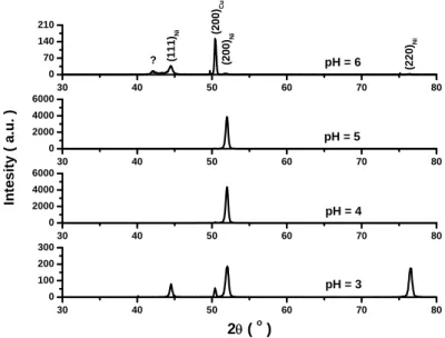
Rolling-recrystallization process to obtain a cube-textured Cu tape was studied. The results show there is a critical rolling deformation rate to obtain a cube textured Cu tape before the final recrystallizing annealing. Other rolling parameters do not influence whether the cube-textured Cu tape is obtained or not, but they would influence the sharpness of cube texture of Cu tape. Studying recrystallization annealing shows the volume fraction of cube texture of Cu tape increases with increasing the annealing temperature, and it also can be found the growth speed of cube texture in Cu tape is very rapid.
A cube-textured Ni layer can be deposited on a cube-textured Cu tape by electro-deposition only if the cathode potential is lower than -0.96V (SEC), and the pH value is the range from 4 to 5, and the temperature of electrolyte is room temperature. It has also been proved that it is impossible that a cube-textured Ni layer is deposited on a cube-textured Cu tape which is polished mechanically.
It is obvious that the magnetic loss induced by Cu-Ni bi-metallic substrate is lower than one induced by Ni-5at%W substrate.
In order to deposit a cube-textured LZO film on metallic substrate, preparation of precursor solution and heat-treatment of precursor film were studied. It is clear that propionic acid is a good solvent for preparing a good precursor solution. A simple sulfuration process was reported to control the orientation of initial LZO layer formed on the surface of metallic substrate. The residual carbon in LZO precursor film is main inhibiting factor to the growth of LZO grains, and increasing the gas speed flowing over the sample is the best way to improve the epitaxial growth of LZO film on metallic substrate.
Key words: coated conductors, Cu-Ni bi-metallic substrate, La2Zr2O7 buffer layer,
1.3.1 Substrate 7
1.3.1.1 Substrate Material 7
1.3.1.2 Fabrication Technologies of Substrates for Coated Conductors 8 1.3.1.3 Required Substrate’s Characteristics 10
1.3.1.4 Brief Summary 11
1.3.2 Buffer Layer 11
1.3.2.1 Buffer Layer Materials 11
1.3.2.2 Fabricating Technologies of Buffer Layer 13
1.3.2.2 Brief Summary 16
1.3.3 YBCO Layer 16
1.3.3.1 TFA-MOD process 16
1.3.3.2 Brief Summary 17
1.4 Summary 17
Chapter II Fabrication of Cube Textured Cu Substrate 18
2.1 Introduction 18
2.2 experiments 18
2.2.1 Preparation of samples 18 2.2.2 Data treatment 19
2.3 Results and Discussions 19 2.3.1 Rolling process 19
2.3.1.1 Influences of rolling deformation rate on the formation of cube texture 20 2.3.1.2 Effect of surface deformation of sample during rolling process 23
2.3.1.3 Influence of thickness reduction per pass on the sharpness of cube texture 25 2.3.1.4 Influence of the rolling direction on the sharpness of cube texture 27
2.3.3 Recrystallization head treatment 28
2.3.2.1 Influence of middle annealing before the final rolling on the texture of Cu substrate 28
2.3.2.2 Influence of annealing temperature on the formation of and sharpness of cube texture 29
2.3.2.3 Influence of annealing time on the formation of and sharpness of cube texture 30
2.3.3 Macroscopic inhomogeneity of cube texture 31 2.3.4 Polishing technology of Cu substrate 32 2.4 Summary 33
Chapter III Deposition of Cube-textured Ni Layer on Cu Substrate by Electro-deposition 34
3.2 Experiments 34
3.3 Results and Discussions 35
3.3.1 Formation of the cube textured electro-deposited Ni layer during the electro-depositing process 35
3.3.1.1 Influence of cathodic potential on texture of Ni layer 35
3.3.1.2 Influence of pH value of electrolyte on the texture of Ni layer 40 3.3.1.3 Influence of electrolyte’s temperature on the texture of Ni layer 41
3.3.1.4 Influence of surface characteristics of Cu substrate on the texture of Ni layer 42 3.3.2 Texture thermal stability of and magnetic property of Cu-Ni bi-metallic substrate 43
3.3.2.1 Thermal stability of texture of Cu-Ni bi-metallic substrate 43 3.3.2.2 Magnetic property of Cu-Ni bi-metallic substrate 44
3.3.3 Characteristics of La2Zr2O7 film deposited on the Cu-Ni bi-metallic substrate 45
3.4 Summary 47
Chapter IV Deposition of La2Zr2O7 Film on Metallic Substrate by Chemical Solution Deposition Process 48
4.1 Introduction 48
4.2 Experiments 48
4.3 Results and Discussions 49
4.3.1 Preparation of Precursor Soluiton 49 4.3.1.1 Choice of solvent 49
4.3.1.2 Pyrolysis characteristics of precursor solution 50
4.3.1.3 Fabrication of LZO phase by the precursor solution 52
4.3.2 Deposition of LZO film on constantan substrate by chemical solution process 55 4.3.2.1 Influences of annealing temperature 55
4.3.2.2 Influences of concentration of precursor solution 56 4.3.2.3 Influences of annealing time 57
4.3.2.4 Influences of heating rate 60 4.4 Summary 63
Chapter V Modification of Surface Characteristics of Metallic Substrate by Sulfuration Process 64
5.1 Introduction 64
5.2 Base of experiment design 64
5.3 Experiments 65
5.4 Results and Discussions 66 5.4.1 Sulfuration Process I 66
5.4.1.1 Sulfuration of Constantan Substrate 66 5.4.1.2 Sulfuration of Ni-5at%W substrate 69 5.4.2 Sulfuration process II 70
5.4.2.1 Sulfuration of Constantan Substrate 70 5.4.2.2 Sulfuration of Ni-5at%W substrate 71
5.4.3 Influence of c(2×2)-S superstructure on the texture of LZO film deposited by chemical solution deposition process 75
5.5 Summary 77
Chapter VI Improvement of Epitaxial Growth of La2Zr2O7 Film on Metallic Substrate 78
6.3.4 Characteristics of LZO film 91 6.3.4.1 Crystal structure of LZO film 91
6.3.4.2 Texture sharpness and surface characteristics of LZO film 92
6.3.5 Deposition of CeO2 layer on LZO film by chemical solution deposition process 95
6.4 Summary 97
Chapter VII Conclusions and Future Works 98 References 101
Introduction
Background
Due to a strong anisotropy of superconducting property of YBa2Cu3Oy (YBCO), large grains
boundary angle results in the problem of “weak link” which means that the intergrain critical current density is lower than the intragrain current density. So to be usable YBCO superconductor in practice all YBCO grains should be arranged along a special orientation. In the early stage of research, it was clear that the melt-textured process was a good method to fabricate the textured YBCO superconductors. But due to the high heat-treatment temperature used in melt-textured process, it can only fabricate bulk superconductors. However, flexible superconducting tapes are necessary in many application fields, for example, motor, cable, magnet, and so on. In order to extend the application field of YBCO superconductors, a method to fabricate YBCO tapes should be developed. In 1990’s, researchers in USA and in Japan found that it was possible to deposit a textured YBCO film on a textured metallic substrate to obtain YBCO tapes. This idea provides a new method to fabricate YBCO superconductors, and extends the application fields of YBCO superconductors.
Comparing with Bi-2223/Ag tapes, YBCO tapes own better superconducting property under a high applied magnetic field. At the same time, the cost of raw materials which are used for fabricating YBCO tapes is cheap because there is no Ag. So it is believed that YBCO tapes will replace the Bi-2223/Ag tapes in future. YBCO tapes are also called coated conductors.
The structure of coated conductors can be divided into four parts: metallic substrate, buffer layer, YBCO layer and protecting layer. The functions of the four parts are as follow: the metallic substrate is a mechanical carrier and origin of texture for coated conductors; the buffer layer prevents diffusion of metallic elements into YBCO layer, and transmits the texture from the metallic substrate to YBCO layer; YBCO layer is the major part which carries the supercurrent; the protecting layer prevents YBCO layer from corrosion and mechanical degradations, it also serves as an electrical shunt.
From the viewpoints of material, the metallic substrate is usually fabricated by Ni-W alloys but hastelloy or steel are also used. Because the Curie temperature of most of Ni-W alloys is higher than 77K, Cu and Cu-based alloys attract interest to many researchers. In a word, material researchers try to develop a cube-textured substrate with lower magnetic property and high mechanical strength. Because the buffer layer should take multi-functions, the architecture of buffer layers is usually composed of two or three oxide layers. In order to simplify the fabrication process of coated conductors and decrease its cost, it is a main challenge for material researchers to simplify the structure of buffer layer. ReBCO superconducting layers are studied, but the attention of researchers is mainly focused on YBCO. The protecting is usually made of Cu layer on top of a Ag layer.
From the viewpoints of fabrication process of each layers, Ion Beam Assisted Deposition (IBAD) process and Rolling Assisted Biaxially Textured Substrate (RABiTS) are the main two methods used to obtain textured substrates. The fabrication process of the buffer layer can be divided into two classes: physical vapor deposition (PVD) and chemical solution deposition (CSD). Because the architecture of the buffer layer is usually composed of two or three oxide layers, a successful architecture of buffer layer is usually fabricated by a combination of multi-technologies. However, with simplifying the structure of buffer layer, it could be foreseen that the use of a single method like CSD process will become possible. It
TFA-MOD process.
So the development of cube-textured metallic substrate with sharp texture and deposition of buffer layer on metallic substrate by CSD process have been studied in this dissertation.
In order to obtain cube-textured metallic substrate with sharp texture and low magnetic property, a new Cu-Ni bi-metallic substrate was developed. The characteristic of this new substrate is that Ni layer is deposited on a cube-textured Cu tape by electro-deposition. After Ni layer is deposited on the Cu tape, it can overcome the disadvantages of pure Cu substrate which has low thermal stability of texture and poor oxidization resistance. The advantages of this new substrate are a sharper cube texture and a low magnetization. After the heat-treatment required by the deposition process of buffer layer and YBCO layer, the interdiffusion of Cu with Ni layer would decrease the global magnetic moment wear by the substrate compared to that of the Ni layer.
We consider La2Zr2O7 (LZO) as a good material for the buffer layer. In order to obtain
cube-textured LZO film with good surface texture and crystallinity on metallic substrate, the nucleation stage and growth stage during deposition of LZO film was considered. Nucleation of an oxide film on a metal surface is not fully understood, it involves the complex formation of ionic/non-ionic interface. On the other hand, a slight irreproducibility in the buffer layer texture is not tolerated for a long YBCO tape. Recently, researchers in United States found that c(2x2)-S superstructure on Ni substrate was of benefit to obtaining a cube-textured oxide film on Ni substrate. But the efficiency of c(2x2)-S superstructure was only proved in PVD process, no body could tell if c(2x2)-S superstructure was useful or not in CSD process. So a simple way to obtain a c(2x2)-S superstructure on metallic substrate was developed firstly, and then its influence on the texture of LZO film was studied.
Due to a large crystallization driving force in CSD process, it is possible that the homogenous nucleation takes place in the bulk and top layer of LZO precursor film. It results in a poor texture on the top layer of final LZO film. This can not be tolerated. The sharp cube texture from bottom to top layer of LZO film, especially surface texture of final LZO film, is necessary. In this dissertation, the thermodynamic analysis about pyrolysis of LZO precursor film was done. Based on this analysis, the epitaxial growth of LZO film was optimized to obtain cube-textured LZO film with good surface texture and crystallinity.
Overview of this dissertation
In previous parts, researching background and research objectives were featured. According to the researching fields in this dissertation, this dissertation is organized in following manner.
Chapter II focuses on the fabrication of sharpe cube-textured Cu substrate.
Chapter III analyzes the process of depositing cube-textured Ni layer on Cu substrate by electro-deposition.
Chapter IV presents how to obtain a good precursor solution for depositing La2Zr2O7(LZO) film, and
reports some results about deposition of LZO film on constantan substrate.
Chapter V introduces a process of obtaining a c(2x2)-S superstructure on metallic substrate, and discuss the influence of c(2x2)-S superstructure on the texture of LZO films.
Chapter VI describes in detail improvement of epitaxial growth of LZO film with a good surface texture and crystallinity on metallic substrate.
superconductor, YBCO superconductor have stronger intrinsic flux pinning force, and good superconducting properties under high magnetic field at 77K. Except for temperature lower than 30K, the critical current density of Bi-2223 superconductor decreases rapidly with increasing the magnetic field. So under high magnetic field at 77K, YBCO superconductor is the best choice. Results in Fig.1.1[3]
compare the irreversibility field of different superconducting materials, it indicates that YBCO superconductor is better than other superconducting material at the boiling point of liquid nitrogen.
Due to the anisotropy of superconducting properties of YBCO and Bi-2223 superconducting material, the first thing that must be done is to control the orientation of grains in order to improve the superconducting properties. Comparing with YBCO material, Bi-2223 grains can be partially textured by cold working and heat-treatment process, and the temperature of processing of Bi-2223 is lower (<850°C)[4-8]. Due to these characteristics, the powder-in-tube process is the main process to fabricate the
Bi-2223 superconductors. This process is inapplicable to fabricate YBCO superconductor with high current density. In order to decrease the “weak-link” induced by large misorientation angle, the melt-textured processes were experimented by many research groups[9-11]. The melting process is a good
way to overcome the “weak-link”, but it needs high annealing temperature (>1015°C), and molten parts can degrade most kind of metals, except Ag and Pt. So the melt-textured process can be used only to fabricate rods of YBCO superconductors. It limits the practical applications of YBCO superconductor. Considering that the main application of superconductors is in the field of cables or magnets, the fabrication of the long tape is the key to the development of YBCO superconductor.
Y.Iijima[12] has fabricated successfully biaxially textured YBCO layer on a flexible metal substrate
by Ion Beam Assisted Deposition (IBAD) process opening a new way to fabricate YBCO superconductors. But IBAD technology has some disadvantages: a high cost and a low deposition speed. Then a new route was discovered by D. Norton [13] and A. Goyal [14] using a cube-textured Ni substrate produced by a rolling-heat treatment process as a template to grow the YBCO layer by epitaxial growth. They named this route of substrate processing “Rolling Assisted Biaxially Textured Substrates” or RABiTS. Due to the outcome of IBAD and RABiTS routes, the YBCO deposited layer on the biaxially textured flexible metal substrate induces the replacement of Bi-2223/Ag tapes, first generation tape. The YBCO tapes are also called coated conductors or G conductors.
Fig. 1.1 Irreversibility field of different superconductorsvs. temperature[3]
1.2 Structure of Coated Conductors and Functions of Substructure
of Coated Conductors
Because of the anisotropic superconducting properties of YBCO, misorientation angle between adjacent grains affects obviously the transport properties of YBCO superconductors (shown in figure 1.2)[15,16]. The orientation of YBCO grains is the first question which must be solved. A c-axial
orientation of YBCO grains is achieved in the melt-textured processes, but at high annealing temperature. But the only control of the orientation of c axes of YBCO grains is not sufficient for carrying high critical current. In order to transport large current, the orientation of YBCO grains must be biaxially textured, that is c axes and a axes of YBCO grains are parallel to each other respectively. In other words, not only c axises of YBCO grains are oriented, but also a or b axes of YBCO grains must be arranged with special orientations. These differences are shown in figure 1.3.
Iijima[12] and Norton[13] succeeded to grow YBCO film on bi-axially textured flexible metals. It not
only solves the orientation of YBCO grains, but also overcomes the disadvantages of melt-textured process. Analyzing their reports shows that a coated conductor can be divided into three main parts: a metal substrate (or flexible template), a buffer layer and a YBCO film. In practice, besides these three layers, a protecting layer is also necessary to prevent the YBCO film from being corroded by different atmospheres or mechanical erosion and also serves as a shunt layer. The figure 1.4 shows the architecture of coated conductor.
Fig. 1.2 Effect of misorientation angle on the Jc value[15]
Fig. 1.3 The texture difference between the melting process and biaxial texture a: Texture after melting process
b: Biaxial texture which is necessary for coated conductor
Fig. 1.4 Architecture of coated conductor
The metal substrate plays the role of a mechanical carrier, but it is also flexible. Another function of the metal substrate is to be used as a template to transmit the texture. The metal substrate is a biaxially textured tape (RABiTS process), or is polycrystalline (IBAD process). If the metal substrate is polycrystalline, the texture is given by the biaxial textured oxide film which is deposited on the polycrystalline metal substrate by IBAD process. Except Ag or Pt, most metallic elements degrade the superconducting properties of YBCO if they diffuse into it. So to prevent such diffusion is essential and the main function of buffer layers. At the same time, buffer layers also prevent oxidation of the metal substrate during the fabrication process of the YBCO layer. Besides the chemical resistance, transmitting the texture and decreasing the lattice mismatch between metal substrate and YBCO are essential functions
of the buffer layers. The YBCO layer is the core of the coated conductor which carries the super-current. The protecting layer prevents the degradation of the properties of YBCO that could be induced by any circumstance. Because the considered buffer layers are oxide, and dielectric, the protection in the case of overcurrents must be considered. So another function of the protecting layer is the electrical stabilization of the tape.
1.3 Choice of Material and Fabrication of Coated Conductors
Recently, most of the researchers focus their work on the three following aspects about coated conductors: fabrication technology of metallic substrates, deposition technologies of buffer layer and deposition technologies of the YBCO layer. The issues related to these three aspects will be discussed below.
1.3.1 Substrate
1.3.1.1 Substrate Material
Coated conductors are obtained by hetero-epitaxial growth of YBCO on the metal substrate with intermediate buffer layers. In order to obtain a bi-axially textured YBCO layer, the metal substrate must have be a single texture component, at the same time the mismatch of crystal lattice between YBCO and the metal substrate must be as small as possible. Ni is a face-centered cubic metal, it is easy to obtain a high volume fraction of cube texture by rolling-heat treatment process. Concerning the mismatch of crystal lattice between YBCO and the metal substrate, due to the parameter of crystal lattice of Ni (0.3524nm), the mismatch with YBCO is –8.57%. So based on the viewpoint of cube texture and mismatch of crystal lattice, Ni is the first candidate of metal substrate material [13, 14, 17, 18]. But pure Ni is
ferromagnetic and mechanically too soft. It is a strong disadvantage in practical application if pure Ni is to be used as substrate. Recently, several research groups focused on the Ni-based alloy, and wanted to increase the mechanical strength and decrease the Curie temperature of Ni-based substrate by alloying. About these Ni-based alloy, for example Ni-W[19-23], Ni-Cr[24,25] and Ni-Cu[26,27] and others, Ni-W alloy
has been highlighted. Considering the decrease the AC loss, a non-ferromagnetic substrate is the best. So
Cu, another face-centered cubic metal, has been considered[28-34]. Compared with Ni, Cu is
non-ferromagnetic, has a high thermal and electric conductivity, and a low cost, but the disadvantages of Cu are a poor thermal-stability of texture, and a poor oxidizing resistance. Depositing a protecting layer on the Cu is a good way to overcome these disadvantages[35-37]. Another candidate is Ag[38-44]. Compared
with Ni and Cu, Ag substrate does not need a buffer layer, YBCO layer can be deposited directly on Ag substrate [38-42] and oxygen can diffuse through sivel to oxidize YBCO at the right stoichiometry.
However its low stacking fault energy making dynamic recrystallization easy during the rolling-annealing process is a great disadvantage to obtain a pure cube texture. Due to this characteristic of Ag, the texture of (110)<110> or (110)<112> is usually formed[43,44]. The Table 1.1 concludes all the review.
Polycrystalline metal can also constitute a substrate for coated conductors using the the IBAD or ISD technology to deposit a first buffer layer able to be a template for the grow of epitaxial YBCO layer[12, 45-49]. This broadens the field of usable metals; for example, stainless steel or hastelloy, can be
chosen for substrate for coated conductors in IBAD or ISD routes. It is an advantage of IBAD and ISD routes that not only face-centered cubic metal or its alloy can be chosen for coated conductors[49].
Su bstrate material Mismatch (% ) te xt ure Th ermo stability of texture magn etic Oxi dization res istance ther mo extension coefficient ch emical co mpatib ility mecha nical propert y cost Ni -8.57 go od go od y es go od 13-1 7.4 w orst sof t medi al Cu -6.10 go od ba d n o wo rst 17 w orst sof t low Ag 6 .10 no rmal ba d n o go od 18.9-25 b etter sof t high
The choice of the best material for coated conductor is still an open question, it is complex since the substrate has several functions. However, some requirements muts be fulfilled like: sharp cube-texture, high mechanical strength and low magnetic moment.
1.3.1.2 Fabrication Technologies of Substrates for Coated Conductors
There are three main technologies to fabricate substrate for coated conductors: Rolling Assisted Biaxially Textured Substrates (RABiTS) process, Ion Beam Assisted Deposition (IBAD) process, and Inclined Substrate Deposition (ISD) process. Recent results show that the first two processes have attracted many researchers.
1.3.1.2.1 Rolling Assisted Biaxially Textured Substrates (RABiTS) process[13,14,19-34,50-53]
After being cold worked and recrystallized by annealing, non-random orientations of grains are found in metals. This defines rolling texture or recrystallization texture respectively. Usually, a cube texture is obtained in a face-centered cubic metal with high stacking fault energy after being cold worked
and submitted to a recrystallization process. That is the base of the RABiTS process. In comparison to other processes, RABiTS process shows a high efficiency and a low cost. Fig. 1.5 shows the schematic plan of RABiTS route. Because of these advantages, many research groups focus on this process[50-53].
Compared to IBAD process, the disadvantage of RABiTS process is that it applies only for face-centered cubic metal with high stacking fault energy while other metals can be used in IBAD process. In the beginning of coated conductor, Ni was chosen in RABiTS process, but Ni-W alloy is now preferred and other Ni-based alloys investigated. Besides Ni-W alloy, some interest has been raised for Cu[28-34].
1.3.1.2.2 Ion Beam Assisted Deposition (IBAD) process[12,45,49,54-56]
It has been proved in the results reported by Fujitsu company [12] that a textured buffer layer can be
deposited on Hastelloy by Ion Beam Assisted Deposition (IBAD) process. In this process, the metal substrate is polycrystalline, and the texture is based on a textured seed layer. So, the substrate is a combination of a metal tape with a textured oxide layer. In the IBAD process, an ion beam assists the deposition of the oxide during the growth of the buffer films. Usually, the assisting ion beam is tilted form the substrate normal by an angle close to 55o. The advantage of IBAD process is to apply to any
metals like Ni-based alloy[12,54-55] and stainless steel[49]. It is very good to fulfill the requirements for
substrate to have high mechanical properties and low magnetic properties. But IBAD has a low fabrication speed and needs a complex equipment. So, only the seed layer is fabricated by the IBAD process[46,57] while other layers are deposited by more economical methods. Fig. 1.6 shows the
mechanism of IBAD process.
Fig. 1.5 a RABiTS route to fabricate coated conductors
Fig. 1.6 IBAD process (cited from Las Alamos)
1.3.1.2.3 Inclined Substrate Deposition (ISD) process[47,48,58,59]
Similar to IBAD process, Inclined Substrate Deposition (ISD) process is a vacuum-based technology to texture an oxide layer on a polycrystalline metal substrate. In ISD process, a textured oxide layer is deposited by using an off-axis pulsed laser ablation without other assisting ion beam. The advantages and disadvantages of ISD process are similar to those of IBAD process. However the surface roughness of the oxide layer deposited by ISD is high. Fig. 1.7 shows the ISD process.
Fig. 1.7 ISD process
(cited from www.ornl.gov/sci/htsc/documents/pdf/CCRoadmap8-23.PDF)
1.3.1.3 Required Substrate’s Characteristics
Based on the uses of the substrates, the first requirement for a substrate is to have a sharp cube texture. The texture is characterized by measurements using ω-scans were ω is the incident angle of the
X-rays, φ-scans where φ is the rotation angle around the normal to the sample, and tilts of the sample (χ) with respect the horizontal axis of the diffractometer. Usually, FWHM (Full Width at Half Maximum) value of ω scan and φ scan are used to quantify the sharpness. Because the texture is 3D, and ω and φ scans only show 1D information, then FWHM of ω and φ scans can not characterize all aspects of the texture’s sharpness. For example, FWHM of ω scan of Ni substrate is different along the rolling direction and transversally to it, thus it depends of φ angle. So researchers in America proposed the concept of a “true in-plane texture”[60] which can be expressed by:
(
ϖ
φ
ϖ
φ
)
χ
φ
φ φ2 90 2 2 2 0 32
tan
cos
sin
= =
−
Δ
Δ
−
Δ
=
ΔΦ
true observed .Where Δφ and Δω are FWHM of φ-scans and ω-scans respectively. Besides this, there have been many questions about how to characterize the texture’s sharpness, this is however beyond the scope of this work.
A second requirement is to have a strong mechanical strength and a low magnetic moment. A strong mechanical strength is required for tapes to support the stretches and the bending imposed during the cabling process. That is why the Ni-5at%W substrate is preferred over pure Ni. A low magnetic substrate is needed to decrease the AC losses resulting from the magnetic properties of the substrate.
Because the epitaxial growth will be used to form the buffer layer on the metallic substrate, the surface characteristics of substrates are important. References showed that a c(2×2)-S superstructure could be formed on the surface of Ni-based substrate[61-63], and this superstructure was needed to obtain a
cube textured oxide layer on metallic substrate[64,65]. So the knowledge of the surface characteristics is
important in order to obtain a good buffer layer on metallic substrates.
Besides surface characteristics, topological properties like grooves, grain boundaries and grains size of the substrates, would indirectly influence the superconducting properties of coated conductors. However, some results[66] show that thermal grooving in substrate influences slightly the Jc value of
coated conductors, while grain boundaries and grain sizes will influence more the Jc value of coated conductors. From the viewpoint of epitaxial growth, the surface roughness of and cleanness of the substrate are also important, but a few results were reported on this apsect.
1.3.1.4 Brief Summary
Based on this review, the development of metallic substrate with low magnetic property, high mechanical property and sharp cube texture is the main effort of research in the field of coated conductors. A comparison of the processes RABiTS, IBAD and ISD shows that RABiTS is the process having the best chance to be used for economic metallic substrates.
1.3.2 Buffer Layer
1.3.2.1 Buffer Layer Materials
The functions of buffer layer require that its characteristics should be as follow: 1) small lattice mismatch with the substrate and with YBCO; 2) no chemical reaction with YBCO and with the substrate; 3) low diffusivity of metals and oxygen; 4) similar thermal expansion coefficient with that of YBCO. Usually, the buffer layer materials can be divided into, conductive buffer layers[67-69] and insulating buffer
(cm/s) YBCO MgO Rocksalt 4.21 9.35 -16.3 8×10-22 CeO2 Fluorite 3.83 -0.52 -7.99 6×10⁻⁹ Y2O3 Mn2O3 3.75 -2.60 -6.03 6×10⁻¹⁰ YSZ Fluorite 3.63 -5.71 -2.92 2×10⁻⁸ SrTiO3 Peroyskite 3.91 1.56 -9.87 --- La2Zr2O7 Pyrochlore 3.81 -1.04 -7.50 --- Gd2Zr2O7 Pyrochlore 3.72 -3.38 -5.27 ---
Note: The mismatch is defined by
M
=
(
a
s−
a
f)
/
a
f , in which as is the lattice parameter of thesubstrate, and af is the lattice parameter of the film. aYBCO = 3.85 Å in mean value.
Fig. 1.8 The lattice change of some oxide and YBCO with changing temperature
Because the buffer layer should satisfy several functions, it is difficult to find an appropriate single material. The architecture of buffer layers is usually composed of two or three different oxide layers. For
example, the buffer layer architecture of CYC [80] is composed of a CeO
2 layer, a Y-stabilized ZrO2 layer
and a CeO2 cap layer. Due to different chemical and physical properties, a combination of
multi-technologies is necessitated to fabricate the buffer layers. The fabrication process of the buffer layers is complex, hard and expensive. So simplifying the buffer layer architecture become an important issue. According to this viewpoint CeO2/RE2Zr2O7 (RE=La, Gd) [46,52,75,81,82] and SrTiO3[67,68,69,73] buffer
layers become very attractives.
1.3.2.2 Fabricating Technologies of Buffer Layer
All the technologies[83] which have been used to fabricate an oxide layer on a substrate can be used
to fabricate the buffer layer. But only some of these are discussed in this section. They can be divided into two main classes: vacuum deposition and chemical solution deposition (CSD).
1.3.2.2.1 Pulsed Laser Deposition process
The pulsed laser deposition (PLD) process is a typical vacuum deposition approach. Many high Tc superconducting film has been fabricated successfully since 1987[82,84-87], and it has become one of the
best method to fabricate superconducting film. In PLD process, the target is ablated by a pulsed laser to form a plasma from which ionic species are deposited on a hot substrate. Because of the high energy of the pulsed laser, all the components in target can be ablated and deposited simultaneously on the substrate. This is very suitable for depositing a complex buffer layer material. At the same time, different targets can be used during the deposition process in order to obtain multi-layers. Fig. 1.9 shows a schematic figure of PLD system.
The disadvantages of PLD process are that it is difficult to fabricate long samples; the cost is high and processing speed slow. So researchers in Japan developed a multi-deposition system to avoid these disadvantages[84].
Fig. 1.10 Schematic diagram of sputtering process
1.3.2.2.2 Sputtering Deposition[51,53,88]
Sputtering deposition is another vacuum deposition approach in which an inert gas is introduced into a vacuum chamber and ionized. The ions bombard the target which is sputtered on the substrate and form the film. In order to increase the sputtering efficiency, a magnetic field is usually applied at the cathode; this technology is also called the magnetron sputtering deposition. The magnetron sputtering can be divided into two classes: direct current sputtering and radio frequency sputtering. Comparing with direct current sputtering, the radio frequency sputtering process does not need a conductive target, so it is often used to fabricate buffer layers of insulating compounds. Fig. 1.10 shows the schematic diagram of sputtering process.
1.3.2.2.3 Chemical Solution Deposition (CSD) Processes
An ultrahigh vacuum device is necessary for vacuum deposition. So it is not appropriate for fabricating economic coated conductors. At the same time, vacuum deposition approaches need complex equipments, and fabricating speed is slow.
Contrasting with vacuum deposition, chemical solution deposition (CSD) processes are economical and easy methods to fabricate buffer layers. No complex equipments are needed and deposition speed is fast and can be real-to-real. Besides this, a characteristic of CSD processes is that it is easy to control the composition of the film by adjusting the stoichioemtry in the precursor solution. So more and more research are being focused on the CSD process[52,70,75,89-92].
The fabrication of a buffer layer by CSD processes includes four basic steps: to prepare a precursor solution, to cover the substrate by spin-coating or dip coating method, to pyrolyze and to crystallize the precursor film. Usually, the last two steps occur in same time. Based on the chemical properties of the precursor solution, the CSD processes can be divided into three classes[93,94]: Sol-gel process,
Metal-organic decomposition (MOD) process and Hybrid routes. The alkoxide precursors are used in Sol-gel process, carboxylates or β-diketonates are used in MOD and combined ligands are used in Hybrid routes.
Whatever the precursors are, the preparation of the precursor solution is a key for CSD processes and the parameters of the process are very sensitive to the properties of the precursor solution. The required characteristics of the precursor solution are: i) sufficient long-term stability; ii) no macroscopic phase separation during drying or pyrolysis; iii) acceptable wetting of the substrate; iv) no reaction with the substrate. If the precursor solution with good properties can be prepared successfully, the next step would be to optimize deposition and the heat-treatment of the precursor film.
Several disadvantages of CSD processes must be however recalled: depositing thick films in one step is not easy without crack formation in the precursor film[95]; surface crystallinity and texture of film
fabricated by CSD processes must be perfect if the film is used to fabricate the buffer layer[96]. However,
results reported by many labs show that CSD process is a potential method to obtain coated conductors with high Jc value. ORNL has obtained several records on YBCO coated conductor with high superconducting properties[81].
1.3.2.2.4 Other Deposition Processes
1.3.2.2.4.1 Metal Organic Chemical Vapor Deposition[71]
Metal organic chemical vapor deposition (MOCVD) uses metal organic materials with high vapor pressure as sources, its vapors obtained at moderate pressure (∼ 5 Torr) are carried into a reaction chamber by an inert gas. A film is obtained by reaction of the different vapor of metal organic materials on the substrate. A high vacuum is not necessary and it is possible to fabricate long tapes in a continuous process. However it is difficult to stabilize the injection of the vapor which will influence the uniformity of the tape[97]. Fig.1.11 is a schematic diagram of MOCVD system.
Fig. 1.11 A schematic diagram of MOCVD system
1: mixed gas chamber; 2: flow meter; 3: motor; 4: manometer; 5: stainless steel pipe; 6: injection head; 7: sample; 8: sample holder; 9: reaction chamber; 10: vacuum pump; 11: temperature controller; 12: heater; 13: adiabatic material; 14: airtight seal
1.3.2.2.4.2 Surface Oxidation Epitaxy Process[77,98,99]
Surface Oxidation Epitaxy (SOE) process [98] has been reported by ISTEC for the fabrication of a
buffer layer in 1999. In this process, the Ni substrate is heated at a high temperature (1000~1300°C) under oxygen or air atmosphere, forming a cube textured NiO layer on the surface of substrate. The NiO
potential methods to fabricate low cost coated conductors with good properties.
1.3.3 YBCO Layer
Except the SOE process, almost all the technologies which were mentioned previously can be used to deposit YBCO layer. Three main processes are used to deposit the YBCO layer: Metal Organic
Decomposition (MOD) process[88, 100 -105], Metal Organic Chemical Vapor Deposition (MOCVD)
process[97, 106, 107,108] and Physical Vapor Deposition (PVD) process[46, 109-112]. Among these technologies,
metal-organic deposition using trifluoroacetates (TFA-MOD) process, is considered as the best candidate for fabricating YBCO layer at atmospheric pressure.
1.3.3.1 TFA-MOD process
The obstacle of fabricating YBCO layer by normal MOD process is BaCO3 that always forms during
normal MOD process. Because the thermal stability of BaCO3 is very large, BaCO3 will impede to reach
high superconducting properties of YBCO layer. However, using trifluoroacetates, BaF2, instead of
BaCO3, is formed during pyrolysis of precursor film. BaF2 can be decomposed easily under humid gas.
So this process using trifluoroacetates can overcome the obstacle which the normal MOD always meets.
This process is called the TFA-MOD process[100]. The up-to-date result[118] shows very high
superconducting performances with YBCO layer reaching 735 A/cm at 77 K.
In the TFA-MOD process[101] a stoichiometric mixture acetates is dissolved into trifluoroacetic acid,
and the solution is refined under decompression to obtain a blue gel with impurities. The blue gel is dissolved into methanol, and the solution is refined under decompression again to remove the impurities. This refining process is repeated several times to obtain a pure precursor solution. The precursor solution is deposited on the substrate and the sample is heated to obtain YBCO layer. The heat treatment is divided in two steps, showed in Fig. 1.12. From Fig. 1.12, it can be seen that the process is very long. So a modified TFA-MOD was reported [102] with a shorter schedule. High Ic values were obtained successfully
Fig. 1.12 The schematic heat-treatment of TFA-MOD process[101]
1.3.3.2 Brief Summary
Besides the Pulsed Laser Deposition process, MOCVD process and MOD process, there are still other alternatives to fabricate YBCO layer, like Pulsed Electron Deposition process[112], Liquid Phase
Epitaxy process[115], BaF
2 ex-situ process[113, 114,116] and Spray pyrolysis process[41,117]. However,
researchers prefer the TFA-MOD process, MOCVD process and PLD process.
1.4 Summary
Due to good superconducting properties under high magnetic field, YBCO coated conductor attracted many researchers efforts. Most attentions on materials are focused on the fabrication of metallic substrate, buffer layer and YBCO layer. Most researchers think that the TFA-MOD process is a potential method to fabricate YBCO layer, but there are still a lot debates concerning the best choice for the metallic substrate, the architecture of the buffer layers and the method for its deposition. However a clear agreement concerns the metallic substrate that should have a sharp cube texture and low magnetic property. Many researchers also agree that the chemical solution deposition is a potential way to fabricate economic coated conductors with good superconducting properties.
ferromagnetic, this is a strong handicap for handling long tapes and for magnetic losses in cables carrying AC current. In order to decrease their magnetic properties, several Ni-based alloys were developed[19-27].
Alloying not only decrease the Curie temperature, but also improve the substrate’s mechanical strength. Although alloying can decrease the magnetic property of Ni-based substrate, the non-magnetic metallic substrate is the best choice in the perspective of cable applications. This is why several researchers[28-34]
have attempted to use Cu substrate .
Cu is a face centered cubic metal like Ni; Cu tapes can be fabricated cube-textured by the rolling-recrystallization process. At the same time, the mismatch of Cu with YBCO is only 5.4 % with the a-axis and 7.1 % with the b-axis. Based on these viewpoints, Cu is an important alternative to nickel based substrates. Besides these, Cu has other advantages, for example, it is cheaper, it has a high thermal conductivity and a low electrical resistance. But the disadvantages of Cu substrate are obvious, the thermal stability of the cube texture and the oxidation resistance of Cu tapes are poor. These weaknesses can be overcome by depositing buffer layers with a special architecture[31,33] or adding a protecting metal
layer[35-37] like a Ni layer. This chapter is focused on the fabrication of cube textured Cu tapes. How to
protect the Cu substrate will be studied in next the chapter.
2.2 Experiments
2.2.1 Preparation of samplesA Cu plate, whose purity was larger than 99.7%, was used as raw material. It was divided in several pieces of different thicknesses: 2.6mm, 4.3mm, and 14mm, respectively. Before rolling, each piece was polished mechanically. The samples were rolled uni-directionally to a final thickness of 0.18mm. The total rolling deformation rates was 93%, 95.8% and 98.7%, respectively. After rolling, all the samples were heat treated under vacuum (total pressure lower than 10-2Pa), and annealed at 600°C with a heating
rate of 1200°C/h.
In order to compare the influence of cold working on the texture of the substrate, Cu rods were also investigated. A copper rod was extruded from an ingot and drawn to reach the diameters of 3.8mm or 10mm respectively, then rolled uni-directionally to reach a final thickness of 0.19mm. In this experiment, the rolling direction was reversed at each end of the sample until the final thickness was reached. All samples were annealed at 600°C for 1 hour under vacuum. Based on the engineering viewpoint, the reversed rolling process is better controlled than the unidirectional rolling. In order to compare these two processes, some Cu rods were chosen to test the influence of changing the rolling direction..
Cu rods (diameter of 10mm) were annealed at different temperatures during different times.
In order to decrease the roughness of the Cu substrates, their surfaces were electro-polished with an electrolyte containing a high concentration, of H3PO4.
2.2.2 Data treatments
Texture, or preferred orientation of crystallites, is an intrinsic feature of materials that influences several of their physical properties. Texture means that the crystallographic orientations are not random. Textures are quantified by the Orientation Distribution Function (ODF) which is defined as:
( )
dV
f g dg
V
=
where: f(g) – is the ODF;g – is the orientation wit respect to the sample’s referential;
dV –is the volume of the crystallites having the orientation g in the element of space orientation dg; V – is the sample’s volume. The ODF can not be obtained directly, ODF calculation is usually calculated from several pole figures by an appropriate algorithm now included in the software of LaboTex.
The characteristics of a texture can be described by its sharpness and volume fraction. Usually, the sharpness of a texture can be quantified by the Full Width at Half Maximum (FWHM) of ω and φ scans. These two terms refers respectively to out-of-plane component of the texture (ω scan) and the in-plane texture component of the texture (φ scan). The volume fraction can be obtained directly from ODF calculation.
In this chapter, all textures were checked by X-ray diffraction (Cu Kα) with a four circles goniometer (Seifert MZ IV equipped with Xenocs multilayer optics, the incident x-ray beam has a horizontal divergence of 0.06°) to measure pole figures, ω and φ scans. Considering that the sample’s texture is not uniform in Euler space, the ω scan were done under conditions where the φ angle was 0o, 90o or varied
(72o/s), which corresponds respectively to measurements performed along the transverse direction, along
the rolling direction and for an average of both.
The values of FWHM of ω and φ scans were obtained by fitting the curves using Gaussian functions (considering the large FWHM of our samples, using other functions more appropriate for x-ray diffraction will have marginal effect on the results) with the software Origin. Raw data were used to plot the pole figures using the software IgorPro, there were no defocusing corrections made in these plots. The Orientation Distribution Function (ODF) was calculated using the software LaboTex after taking into account the defocusing corrections calculated from a pole figure of a Cu powder free of texture.
2.3 Results and Discussions
2.3.1 Rolling processThe fabrication process of cube textured Cu substrate can be divided in two main steps: rolling and recrystallization. Several parameters of the process influence the final texture of Cu tapes. The influences of rolling process will be discussed first in this part
shear texture component[122,123], the amount of which increases with the rolling deformation rate. The
influence of the shear texture contribution will be discussed later.
Fig. 2.1 The texture of raw Cu plates
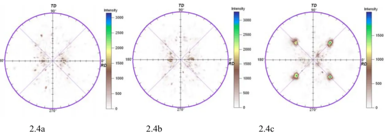
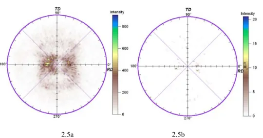
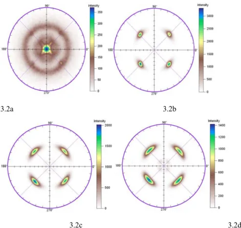
The texture after annealing at 600°C for 1 h is shown in Fig. 2.4. A comparison of Fig 2.4a, Fig 2.4b and Fig 2.4c shows that the cube texture can be found only in sample which was rolled with a deformation rate of 98.7%. Annealing at 600°C of samples deformed only at 95.8% does not provide the cube texture. In order to know if this is due to the heat treatment, these samples were annealed at 300Ԩ or 700Ԩ for 2 hours, and then their texture were compared. It is clear from Fig.2.5 that the cube texture can not be found in both samples showing that 700°C is not sufficient to crystallize the cube texture for this low deformation rate. Combining Fig 2.4 and Fig 2.5 shows that the rolling process is a key to obtain cube textured Cu tapes. Only sufficiently large deformation rate is able to induce cube texture after recrystallization. The deformation rate must be larger than a critical value as suggested before in ref. [29]. In our case, the critical value is larger than 95.8 %, while it was found equal to 83 % in ref. [29]. Ref. [28] also studied the influence of the rolling process on the texture of Cu tapes made from a raw Cu plate. These authors were unable to reach the cube texture. We think that the difference between these experiments is due to differences in the thermal/mechanical process applied. The Cu plate treated in ref. [28] was submitted to a series of deformation and heat treatments, because the recrystallization temperature of Cu is very low (~150°C), the texture of the starting Cu plate was not random. Based on the above-mentioned analysis, we can conclude that the final annealing texture of Cu is very sensitive to the rolling-annealing process.
2.2a 2.2b 2.2c
Fig 2.2 (111) pole figures of Cu tapes after rolling at different deformation rate 2.2a: 93%; 2.2b: 95.8%; 2.2c: 98.7%
Fig. 2.3 (111) pole figure of Cu rolled[124]
Texture components: × S component; Ο C component; • B component; ◊ G component; □ cube texture
2.4a 2.4b 2.4c
Fig. 2.4 Influence of the rolling deformation rate on the recrystallization texture of Cu tapes. 2.4a 93%; 2.4b: 95.8%; 2.4c: 98.7%
2.5a 2.5b
Fig. 2.5 Influence of annealing temperature on the recrystallization texture of Cu tapes with a rolling deformation rate of 95.8%. 2.5a: 300°C; 2.5b: 700°C.
B: Cu rods
In order to know more on how is influenced the formation of cube texture by the deformation rate, Cu rods with different diameter (φ = 3.8 mm and φ = 10 mm) were studied. They were submitted to the same process as described previously. The sample’s textures are shown in Fig. 2.6, where the raw diameter of the samples are φ = 3.8mm in Fig. 2.6a, and φ = 10mm Fig. 2.6b respectively. These figures show that the cube texture can be obtained only if the Cu rod were heavily deformed. These results stress that a heavy rolling deformation is a key to obtain cube textured Cu tapes.
2.6a 2.6b
Fig. 2.6 Influence of the rolling deformation on the texture of Cu tapes. Raw material is a rod rolled to a final thickness of 0.19 mm.
2.3.1.2 Effect of surface deformation during rolling process
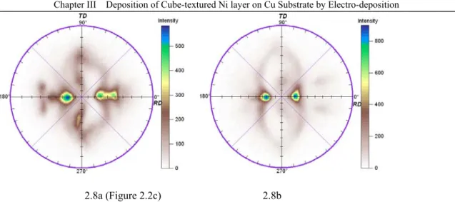
Friction between roller and sample results in a non uniform texture across the sample thickness. This is linked to the roller gap geometry which is defined by the ratio l/h, where l is the projected length of contact between roller and sample, and h is the mean thickness of sample. Friction causes shear stress in the surface layer resulting in shear texture. Shear texture must be distinguished from non uniformity in the texture caused by the roller gap. Fig.2.7 shows a typical shear texture. Compared to rolled texture, the characteristic of a shear texture is in the position of the diffraction spot which shifts from χ=25º to 52º in the RD direction while the contribution is broadened along the TD. After removing the top layer of the sample in Fig. 2.2c (0.001 mm), the (111) pole figure was measured again. The result shows a typical rolling texture of high stacking energy FCC metal (Fig. 2.8b). The calculation of l/h shows that the value of the roller gap increases with decreasing thickness of sample for constant thickness reduction per pass, and the value of l/h is larger than 5 if the thickness of the sample is smaller than 0.74 mm. Under this condition, a shear texture occurs easily in the surface layer[122]. At the same time, the amount of shear
texture becomes large with increasing the rolling deformation rate. This is well evidenced in Fig. 2.2. Besides the rolling deformation rate, the thickness reduction per pass also influences the amount of shear texture. Fig. 2.9 shows this influence, in which the thickness reduction per pass of sample in Fig. 2.9a is 10 %, and 30 % in Fig. 2.9b. It is clear that the larger the thickness reduction per pass, the larger the shear texture contribution is. This is due to the increase of friction when the thickness reduction per pass is increased, this is quantified by l/h increasing from 5.3 for a reduction rate of 10 % to 8.5 when the reduction rate is 30 %.
2.8a (Figure 2.2c) 2.8b
Fig. 2.8 Comparison of (111) pole figures of sample in figure 2.2 before and after removing 0.001mm of the top layer. 2.8a: before; 2.8b: after
2.9a 2.9b
Fig. 2.9 Role of thickness reduction per pass. (111) pole figures of samples rolled with a deformation rate of 93%. 2.9a: the thickness reduction per pass is 10 %; 2.9b: the thickness reduction per pass is 30 %
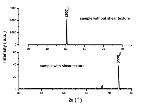
Based on the results of Fig. 2.4, it is qualitatively clear that the formation of cube texture is not influenced by the occurrence of shear texture if the rolling deformation rate is large enough. But a shear texture will contribute to decrease the volume fraction of cube texture; this is the case in the sample of Fig.2.4b. Besides this influence, the shear texture also influences the annealing procedure to obtain a cube texture. The Fig. 2.10 compares θ-2θ scans of two samples recrystallised at 800°C for half hour, the sample on the top was exempt of shear texture while the sample at bottom had a shear texture. It is clear that a cube texture is only found in the sample without shear texture.
30 40 50 60 70 80 0
20 40 60
sample without shear texture
sample with shear texture
(2 20 )Cu Intens ity ( a.u. ) 2θ ( o ) 30 40 50 60 70 80 0 2000 4000 6000 (200 )Cu
Fig. 2.10 Influence of shear texture on the formation of cube texture. Both samples were annealed at 800°C for half hour.
2.3.1.3 Influence of thickness reduction per pass on the sharpness of cube texture
Rolling and recrystallization textures have been investigated for many years but very few concerned the influence of thickness reduction per pass on the sharpness of cube texture. So we investigate this influence in this section.
The shear texture can be always found after Cu plates were heavily rolled even for small thickness reduction per pass, i.e. 10 %. It means that the texture of deformation of Cu plates is inhomogeneous at a macroscopic scale. In order to eliminate this influence we investigated the rolling process of Cu rods was.
A Cu rode with a diameter of φ = 10 mm was rolled with a thickness reduction per pass of 10% or 30%. The Fig. 2.11 shows the (111) pole figures of both rolled samples. It is clear that the patterns of Fig. 2.11 are similar with the one of Fig. 2.3 (ref.[124]) with S component and C component being the major texture components of the texture.
2.11a 2.11b
Fig. 2.11 Influence of thickness reduction per pass on the rolling texture. 2.11a: thickness reduction per pass of 10%; 2.11b: thickness reduction per pass of 30%
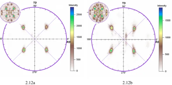
2.12a 2.12b
Fig. 2.12 (111) pole figures of recrystallized samples rolled under a different thickness reduction per pass. 2.12a: thickness reduction per pass of 10%,. 2.12b: thickness reduction per pass of 30%. In both cases, the insert shows the pole figure represented with a log scale for z axis.
The samples were annealed at 600°C for 1 hour and their (111) pole figures are shown in Fig. 2.12. Fig. 2.12a shows a sample rolled under a low thickness reduction per pass (10 %) and compared in Fig. 2.12b with a sample rolled with a high thickness reduction per pass (30 %). These figures are similar at first sight. However there is more twinning components of cube texture when the reduction per pass is larger, Fig .2.12b. Twinning is evidenced by diffracted intensities visible at φ = 45° (and equivalent positions) and χ=15.8o . Moreover, in addition to cube texture and twinning components, some extra
component arises for large thickness reduction per pass (see insert of Fig. 2.12).
The table 2.1 lists the full with at half maximum (FWHM) for ω and φ scans. These data show that the thickness reduction per pass does not influence very much the sharpness of the in-plane texture (φ scan), but has a significant influence on the sharpness of out-of-plane texture (ω scan), especially for φ = 0o .
Table 2.1 Influence of thickness reduction per pass on the sharpness of cube texture of Cu tape Thickness reduction per pass FWHM value of ω scan ( o ) FWHM value of φ scan ( o ) φ = 0o φ = 90o φ = rotation 10% 7.9 4.5 6.3 7.0 30% 9.2 3.1 9.1 7.5
Note: “rotation”means that the sample rotates around the φ axis (72o/s)
Because FWHM for in-plane texture represents the spread of the orientation distribution of <200> direction, it is observed that large reduction per pass affects more the transverse direction (φ = 0) than the rolling direction. We think that this phenomenon is related to the friction between the roller and the sample. During the rolling, the sample expand at each rolling pass. The friction along the transverse direction is increased and this amplified by increasing the reduction per pass. It results in a decrease of the texture sharpness along the transverse direction.
2.13a 2.13b
Fig. 2.13 (111) pole figures of two samples submitted to different rolling process. 2.13a unidirectional rolling. 2.13b reversed rolling. In both cases, the insert shows the pole figure represented with a log scale for z axis.
2.3.1.4 Influence of the rolling direction on the sharpness of cube texture
The unidirectional rolling is the best way to obtain cube textured Ni substrate. But it is necessary in practice to change two times the roller gap at each pass. This is complex and makes the control of the rolling process difficult. So the reversed rolling is more convenient and we investigated it.
Fig. 2.13 and Table 2.2 show the influence the two procedures on a Cu rods with diameter of φ = 10 mm rolled to a final thickness of 0.19 mm with a thickness reduction per pass of 10%, and recrystallized. The
Reversed rolling 8.7 3.4 6.2 6.5 Note: “rotation”means that the sample rotates around the φ axis (72 o/s)
2.3.2 Recrystallization heat treatment
The influences of rolling parameters on formation and sharpness of cube textures were studied in the last section. In this section, the influences of recrystallization on the sharpness of cube texture will be discussed.
2.3.2.1 Influence of pre-annealing on the texture of Cu substrate
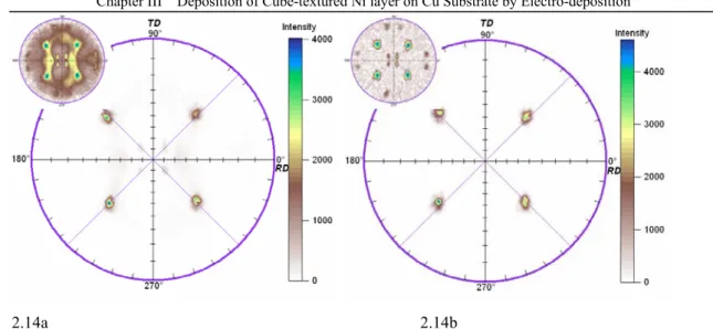
Usually some pre-annealing treatments are made during the cold working performed to process Cu tapes. In order to study the influence of pre-annealing on the sharpness of the cube texture, Cu rods with diameter φ = 10 mm were pre-annealed at 400°C, and then rolled and recrystallized. Typical (111) pole figures of these samples are shown in Fig. 2.14. When a pre-annealing at 400°C is made before rolling, the texture is composed of rolling texture plus cube texture plus twinning, Fig.2.14a. Clearly the cube texture has been formed before the recrystallization treatment. The recrystallisation treatment, makes the rolling texture to disappear but still some twinning remain. Combination the results in Fig. 2.14 and one in Fig. 2.6 shows the rolling deformation rate before the final recrystallization is very important for formation of cube texture, the pre-annealing process does not influence the formation of cube texture if the rolling deformation rate before the final recrystallization is larger a critical rate.
Although, the pre-annealing process does not impede the cube texture formation, it influences the sharpness of cube texture. All the results have listed in Table 2.3. It is surprising that the FWHM value of ω scan is very large if the measurement condition is that the sample rotates about the φ axis. There is no reasonable explanation to explain this result, and more analysis should be done in future.
Table 2.3 Influence of pre-annealing before rolling on the sharpness of cube texture of Cu tape
Pre-annealing FWHM value of ω scan (
o ) FWHM value of φ scan ( o ) φ = 0o φ = 90o φ = rotation Yes 6.8 4.3 9.9 6.4 No 7.9 4.5 6.3 7.0
2.14a 2.14b
Fig. 2.14 Influence of a pre-annealing at 400°C before rolling on the formation of cube texture. 2.14a: rolling texture. 2.14b: annealed texture. In both cases, the insert shows the pole figure represented with a log scale for z axis.
2.3.2.2 Influence of annealing temperature on the formation of and sharpness of cube texture
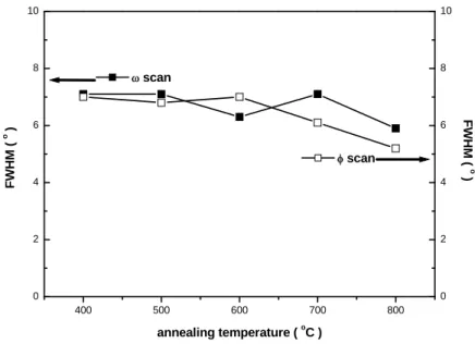
Fig. 2.15 shows the texture of annealed Cu substrates made from Cu rods. The Cu rods had a diameter of φ = 10 mm and were rolled to 0.19 mm with a thickness reduction per pass of 10%, and then annealed at different temperatures for 1 hour. From this figure, it is obvious that the range of annealing temperature to obtain the cube textured Cu substrates is very broad if the rolling deformation rate is large enough. Using a quantified analysis using ODF, the volume fraction of cube texture was calculated, it increases with increasing the annealing temperature, fig.2.16. The results show that the volume fraction of cube texture increases form 65 % to 97.5 % when the annealing temperature is increased from 400°C to 800°C.
A high volume fraction of cube texture is one requirements for Cu substrate but its the sharpness is also important. The effect of annealing temperature on the sharpness of cube texture is shown in Fig. 2.17. The results indicate that the cube texture becomes sharper with increasing annealing temperatures. But this effect is less rapid than the variation of the volume fraction of cube texture. The difference of FWHM value for out-of-plane texture is about 1o, and for in-plane texture is only 2o while the difference of
volume fraction of cube texture is larger than 50%.
2.15a 2.15b 2.15c
Fig. 2.15 Influence of annealing temperatures on the formation of cube texture. 2.15a annealing at 400°C;2.15b annealing at 600°C;2.15c annealing at 800°C.In each of these figures, the insert shows the pole figure represented with a log scale for z axis.
400 500 600 700 800 0 20 V o lu m annealing temperature ( oC )
Fig. 2.16 The volume fraction of cube texture and of cube twin vs. annealing temperature
400 500 600 700 800 0 2 4 6 8 10 ω scan FWHM ( o ) FWHM ( o ) annealing temperature ( oC ) 0 2 4 6 8 10 φ scan
Fig. 2.17 Sharpness of cube texture of Cu tape vs. annealing temperature
2.3.2.3 Influence of annealing time on the formation and sharpness of the cube texture
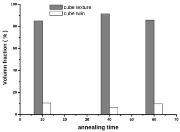
Fig. 2.18 shows the annealing texture of Cu substrate versus time for Cu rods. The Cu rods had a diameter of φ = 10 mm and were rolled to 0.19 mm with a thickness reduction per pass of 10 %, and then annealed at 600°C for different times. The results show that the kinetic of cube texture formation is fast, the cube texture volume fraction reaches 85% in the first 10min and does not change much after (6 % between 10 min and 60 min). The annealing time has only a small influence on the cube texture volume fraction.
0 10 20 30 40 50 60 70 0 20 40 60 80 100 Vol u mn fracti on ( % ) annealing time cube texture cube twin
Fig. 2.18 The cube texture volume fraction vs. the annealing time
Table 2.4 Influence of the annealing time on the sharpness of cube texture of Cu tape Annealing time (min) FWHM value of ω scan ( o ) FWHM value of φ scan ( o ) φ = 0o φ = 90o φ = rotation 10 8.2 3.4 5.2 6.5 40 7.2 3.4 5.6 6.4 60 8.7 3.4 6.2 6.5
Note: “rotation”means that the sample rotates around the φ axis (72 o/s).
Table 2.4 shows the influence of the annealing time on the sharpness of cube texture of Cu substrate. The results show no influence of the annealing time. A comparison of all results shows that the annealing time of 40min is best.
A combination of Fig. 2.16, Fig. 2.18 and Table 2.4 shows that the volume fraction of and the sharpness of cube texture of Cu substrate are less sensitive to annealing time that to annealing temperature.
2.3.3 Macroscopic inhomogeneity of cube texture
During the rolling process, the stress state is different at the top surface and in the bulk. This results in macroscopic inhomogeneities in the rolling texture with thickness. Ref. [122,123] showed that there is a texture gradient across the sample. Our results also show a difference between the surface and the bulk (Fig.2.8). Maybe this macroscopic inhomogeneity of rolling texture will induce an inhomogeneity in the cube texture after annealing.
Table 2.5 compares the sharpness of cube texture of as-received samples to the sharpness of cube texture of a sample which thickness was reduced by 10% by polishing. The results show that there is very little advantage to remove the top surface. However, the roughness must be as small as possible and then
Note: “rotation”means that the sample rotates around the φ axis (72 o/s)
2.3.4 Polishing technology of Cu substrate
The polishing process can be mechanical or electrolytic. Because mechanical polishing is not suitable for depositing a cube textured Ni layer on the Cu substrates by electro-deposition (this will be shown in the next chapter), Cu tapes was polished by electro-polishing.
-0.5 0.0 0.5 1.0 1.5 2.0 0.000 0.004 0.008 0.012 0.016
anode potential window
C
u
rre
nt
( A )
anodic potential vs. SCE ( V )
Fig. 2.19 The graph of anode current versus anodic potential.
Fig. 2.19 shows the graph of anodic current versus anodic potential. According to Fig. 2.19, the range of anodic potential should be from 0.7V (SEC) to 1.6V (SEC) in order to reduce the surface roughness. Because a high anodic potential is faster, we choose an anodic potential of 1.4V (SEC). Fig. 2.20 compares the sample’s surface morphology of the polished zone to that of the un-polished one; Fig. 2.21 shows the morphology by AFM. The results show a clear improvement of the roughness after electro-polishing, but still some sharp peaks remain at a microscale which origin are unclear. The AFM show that the roughness is 8nm (Rrms) at a scale of 40μm × 40μm, and only 1nm ( Rrms) if one excluding