HAL Id: hal-02446833
https://hal.archives-ouvertes.fr/hal-02446833
Submitted on 1 Apr 2021
HAL is a multi-disciplinary open access
archive for the deposit and dissemination of
sci-entific research documents, whether they are
pub-lished or not. The documents may come from
teaching and research institutions in France or
abroad, or from public or private research centers.
L’archive ouverte pluridisciplinaire HAL, est
destinée au dépôt et à la diffusion de documents
scientifiques de niveau recherche, publiés ou non,
émanant des établissements d’enseignement et de
recherche français ou étrangers, des laboratoires
publics ou privés.
Exploiting Transistor Folding Layout as RHBD
technique against Single Event Transients
Y. Q. Aguiar, Frédéric Wrobel, J.-L. Autran, F. L. Kastensmidt, P. Leroux, F.
Saigné, V. Pouget, Antoine Touboul
To cite this version:
Y. Q. Aguiar, Frédéric Wrobel, J.-L. Autran, F. L. Kastensmidt, P. Leroux, et al.. Exploiting
Tran-sistor Folding Layout as RHBD technique against Single Event Transients. IEEE RADECS 2019, Sep
2019, Montpellier, France. pp.1581 - 1589, �10.1109/tns.2020.3003166�. �hal-02446833�
1
Abstract— Radiation hardening techniques can be extensively used in the design level to improve the robustness of VLSI circuits used in space applications. Accordingly, this work analyzes the efficiency of transistor folding layout in improving the Single-Event Transient robustness of digital circuits. Additionally, diffusion splitting is proposed to reduce the area overhead of multiple-finger designs. Besides increasing threshold Linear Energy Transfer, results show that both techniques can also reduce the overall cross-section and the in-orbit SET rate for protons and heavy ions in LEO and ISS orbits.
Index Terms—Transistor Folding, Radiation Hardening by Design (RHBD), Single-Event Transient, Monte-Carlo simulation, Circuit Design
I. INTRODUCTION
HE susceptibility to energetic particles increases as the transistor feature size is reduced [1-3]. Due to the extensive usage of electronics systems in harsh environments, mitigation techniques against radiation effects have been vastly investigated in literature [4-7]. Radiation hardening strategies can be explored from fabrication process modifications to different design implementations. Modifications of doping profiles, optimization of deposition processes and usage of different materials are examples of well-known Radiation Hardening by Process (RHBP) techniques. However, besides its higher cost, RHBP are typically several generations behind the state-of-the-art CMOS process, leading to low-grade performance. On the other hand, Radiation Hardening by Design (RHBD) has been shown to be effective in providing hardness to radiation effects [7]. These techniques can be implemented in different levels of abstraction from circuit layout to system design. The generation mechanisms of Single-Event Effects (SEEs) are strongly connected to the physical layout of integrated circuits (ICs), as, for example, the relation between the energy deposition and charge collection in the p-n junctions of transistors. Accordingly, several hardening approaches can be applied at circuit layout level such as the Enclosed Layout Transistor (ELT), guard rings, dummy transistors/gate or Dual Interlocked Storage Cells (DICE) [6-9].
Manuscript received April 15, 2019. This work was realized within RADSAGA project and has received funding from the European Union’s Horizon 2020 research and innovation programme under the Marie-Skolodowska-Curie grant agreement number 721624.
Y. Q. Aguiar, F. Wrobel, F. Saigné, A. D. Touboul and V. Pouget are with Université de Montpellier, IES – UMR UM/CNRS 5214, 860 Rue de St Priest, Bat. 5, F-34097 Montpellier, France (corresponding author e-mail:
The general goal of each technique is to reduce the charge collection efficiency of a given circuit so the overall Single-Event Transient (SET) pulse can be shortened and/or the collected charge does not exceed the critical charge. For instance, it can be acquired by reducing the sensitive collecting layout area (drain regions) and the parasitic bipolar effect, or even by promoting the pulse quenching effect via charge sharing. However, due to the multi-node collection at deeply scaled technologies, the charge sharing effect might also reduce the efficiency of well-known RHBD schemes such as the DICE designs and Error-Correction Codes (ECCs) due to multiple Single-Event Upset (SEU) and multiple SET occurrences [10]. Some investigation has been done towards the adoption of transistor folding technique as radiation hardening approach [6, 11-13]. Device level simulations and laser testing have shown a reduction on the SET susceptibility of single transistors and inverters [6, 11-13]. However, further study is needed to verify the applicability of this technique to harden a set of standard-cell logic circuits, for instance.
Accordingly, this work proposes the evaluation of the impact of a widely used layout technique, named transistor folding [14], to the SET robustness of basics logic circuits combined with diffusion splitting. The layout technique is adopted in different digital logic gates and its SET susceptibility is evaluated under heavy ions. A layout-based prediction methodology is used to calculate the SET cross-section through Monte Carlo simulations [15, 16]. Further, the in-orbit SET rates are predicted with OMERE package [17] for heavy ions and protons in Low-Earth Orbit (LEO) and International Space Station (ISS) orbits. Proton-induced SET rates are calculated from the heavy ion data using the METIS method [18, 19]. Besides exploiting the transistor folding technique, the novelty of this work also lays on the usage of transistor folding with split in the active area of the transistors on different combinational logic gates to reduce area overhead.
The paper is organized as follows: Section II presents the transistor folding layout technique and the state-of-the-art of RHBD techniques tackling the generation of SET; the sensitivity analysis methodology adopted is described in Section III; the results and discussions on the impact of folded
F. L. Kastensmidt is with in the Instituto de Informática at Universidade Federal do Rio Grande do Sul (UFRGS), Porto Alegre, Brazil
J-L. Autran is with the Institut Materiaux Microelectronique Nanoscience de Provence, Aix-Marseille University, Marseille, France.
P. Leroux is with the Advanced Integrated Sensing Lab, KU Leuven University, Leuven, Belgium.
Exploiting Transistor Folding Layout as RHBD
Technique against Single-Event Transients
Y. Q. Aguiar, F. Wrobel, J-L. Autran, F. L. Kastensmidt, P. Leroux, F. Saigné, V. Pouget and A. D.
Touboul
T
Transients," in IEEE Transactions on Nuclear Science, vol. 67, no. 7, pp. 1581-1589, July 2020, doi: 10.1109/TNS.2020.3003166.
2
transistor in the cross-section of standard cells, the usage of asymmetric layout and voltage variability are provided in Section IV; and, Section V summarizes and concludes this paper.
II. TRANSISTOR FOLDING LAYOUT TECHNIQUE
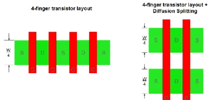
Transistor folding is widely used to achieve improved performance and regularity in VLSI circuits [14]. When larger transistors need to be employed, but it exceeds the fixed cell height of a given design, the transistor folding layout technique is used. The folding technique consists in connecting parallel transistors with reduced channel width to achieve a large overall width. Given a transistor with a channel width W, the same W/L ratio, thus the same drive strength, can be achieved by connecting n transistors with width W/n. Fig. 1 presents the principle of folded transistor layouts in the case of a double-finger transistor. This layout technique divides the drain and source area into smaller partitions depending on the number of fingers. Due to the reduced source and drain areas, the diffusion-to-well capacitance is also reduced.
Considering radiation effects, this technique provides a reduced collecting drain area maintaining the same drive strength. The transistor size of folded designs can be calculated following Eq. 1, where WF is the width of each folded transistor,
NF is the number of fingers, and W is the transistor width in the original design.
𝑊
𝐹=
1𝑁𝐹
× 𝑊 (1)
The transistor folding technique can be adopted along with other hardening techniques such as gate sizing or dummy transistors/gates. The work in [11] was the first to propose transistor folding along with gate sizing to harden a circuit against both SEUs and SETs. A 3D mixed-mode TCAD (Technology Computer-Aided Design) simulation was carried out to analyze the SET pulse characteristics considering alpha particle and heavy ions hit on the center of the drain junctions [11]. Different from the sizing approach, which increases the circuit drive strength at the cost of increased drain area, transistor folding is able to reduce the transistor drain area while keeping the same drive strength. The transistor sizing was able to improve the robustness only for low-energy particles while the transistor folding showed also improvement when considering high-energy particles [11]. In [12], different well structures and layout topologies were studied to evaluate the Propagation Induced Pulse Broadening (PIPB) effect in inverter chains. Accordingly, a double-finger inverter chain was
compared against a single-finger inverter chain. In agreement with [11], the heavy ion results show a reduction on the overall SET pulse width, but minimum influence in the PIPB effect. Inverter chains hardened with guard rings were also evaluated using single and double-finger layout configurations with laser irradiation in [6]. Again, results showed an insignificant pulse-broadening factor for the folded inverter chain, however, a wider SET pulse width average was observed [6]. The authors attributed this to the larger spacing between the drain junctions and the guard rings in the folded design, which limits the charge collection reduction provided by the guard rings. Most of the studies have provided analysis for chains of inverters, and mainly for 2-finger layout configurations. In this work, the transistor folding is adopted on an inverter, NAND and NOR gates, and analyzed through layout-based predictive Monte Carlo simulations. Furthermore, the analysis of diffusion splitting along with transistor folding is provided to overcome the area overhead of multiple-finger designs.
III. METHODOLOGY
The target circuit layouts were designed following a commercial Process Design Kit (PDK) in a bulk 65-nm technology. Additionally, all designs are compatible with a standard-cell library. Minimum width, spacing and alignment/symmetry of each layer is carefully addressed to provide compatibility among the standard cells. The cell height is set to 13 tracks of metal pitch, i.e. 2.6 µm high. To provide flexibility in cell routing, the metal 1 (M1) is primarily used for the intra-cell connections, except for some cases in which metal 2 (M2) is used horizontally. The PMOS transistor width is 760 nm while the NMOS transistor width is 540 nm. To analyze exclusively the impact of the folded layouts, the equivalent transistor sizing was kept the same for all cases. After all circuit designs are DRC (Design Rule Check) clean, LVS (Layout Versus Schematic) checked and logic and electrical characterization is performed, the collecting drain area information can be extracted from the GDS (Graphical Design System) format file and submitted to the MC-Oracle tool [15]. The proposed layout-based predictive simulation chain is divided into two steps: first, particle interaction simulations are performed using the Monte Carlo simulation tool, MC-Oracle [15][20], to calculate and generate an SET database containing all transient currents; second, SPICE electrical simulations are performed to account for the circuit response effects [16, 21- 23]. All circuits were driving a fan-out 1 (FO1), i.e. an inverter was coupled to its output signal. Only the SET pulses with peak voltage higher than 0.6 V (half the supply voltage) are considered for the cross-section calculation. In addition to the double-finger designs (Fig. 1), quadruple-finger layout configurations are also considered in this work (Fig. 2). However, one of the drawbacks of increasing the number of fingers in the folding technique is the increase in layout area. Thus, to overcome the area increase, a Diffusion Splitting (DS) layout technique is proposed and shown in Fig. 2. Instead of using a single strip of active diffusion, a 2-row stacked diffusion transistor is used. Besides reducing the area overhead of the folding technique, DS improves the metal connection routability maintaining the same W/L ratio and the number of gate fingers. To deepen this analysis, the impact on the in-orbit
SET rates for heavy ions and protons and the effect of voltage fluctuation are also presented.
IV. RESULTS AND DISCUSSION
This work analyzes the applicability of the transistor folding layout technique to be used as an RHBD technique in standard-cell libraries. The layout area information for the original design of the inverter, NAND and NOR gate along with the increase factor for its folded designs is shown in Table I. For the three cells analyzed, the double-finger layout configuration exhibited an area increase of approximately 1.5x the original single-finger layout area.
An area increase around 2.5x is expected when using quadruple-finger layout designs. However, if DS is used, the area overhead for the 4-finger designs can be reduced to the same observed in the 2-finger designs, i.e. approximately 1.5x greater than the original designs. Thus, DS provides an area reduction of 36% and 42% for the 4-finger inverter and NAND/NOR cells, respectively.
In Fig. 3, the simplified layout of the NAND designs containing only the metal1, diffusion and poly layers are shown. In standard-cell methodology, a fixed cell height is defined to provide regularity. Thus, as the number of finger is increased, the cell width is increased and, consequently, the cell layout increases. As the transistor sizing is kept the same, the diffusion splitting can be applied to reduce the impact in the layout area, as shown in the Fig. 3.
A. Impact on SET cross-section
σ
SETThe SET cross-section
σ
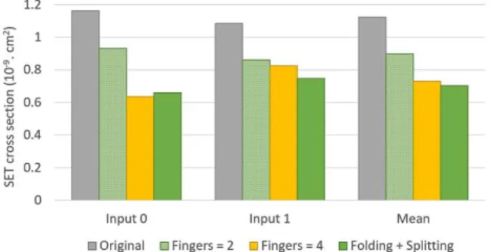
SET for the inverter designs underparticle LET of 78.23 MeV.cm2/mg is shown in Fig. 4. The
folded designs have shown similar
σ
SET for input 1 and input 0,thus using transistor folding may reduce the SET sensitivity dependence on the input signal in the inverter design at high LET. On average, the folded designs provide lower sensitivity then the original design with the greatest
σ
SET reduction for the2-finger layout configuration, approximately 42%. The 4-finger inverter shows improvement solely for the input 1, however, despite the area reduction, DS also reduced the
σ
SET. To analyzethe folding impact for low particle LET irradiation, Fig. 5 presents the SET cross-section for the inverter designs considering heavy ions with LET = 5.43 MeV.cm2/mg. In this
case, the greatest
σ
SET reduction is observed for the 4-fingerinverter with DS, about 37%. It can be observed that, for low LET, the
σ
SET reduces with the increase of the number of fingersNF, in agreement with 3D TCAD results obtained in [11]. As
NF increases, the collecting regions are reduced and sparsely
distributed along the layout, then the charge sharing at low LET is limited. Thus, less folded transistors are affected by a single particle hit, leading to an improvement in the efficiency of the technique in reducing the
σ
SET. Fig. 6 depicts the mean SETTABLEI
TOTAL AREA FOR EACH ORIGINAL CELL LAYOUT DESIGN (µM2) AND THE INCREASE FACTOR FOR ITS CORRESPONDENT FOLDED DESIGNS
Original design (µm2)
Folded designs 2-finger 4-finger 4-finger
with DS
Inverter 1.560 ~1.5x ~2.4x ~1.5x
NAND2 2.444 ~1.5x ~2.6x ~1.5x
NOR2 2.444 ~1.5x ~2.6x ~1.5x
Fig. 3. Simplified layout design of NAND F0 (no folding), NAND F2 (2-finger design), NAND F4 (4-finger design) and NAND F4S (4-finger design with Diffusion Splitting). For clarity, only the metal1, diffusion and poly layers are shown.
Fig. 2. Standard quadruple-finger folded transistor layout vs. folded transistor layout with Diffusion Splitting (DS) technique in which the diffusion strip is split into 2 strips and placed vertically aligned within each other.
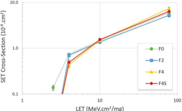
4
cross-section curve for each inverter cell design considering the input 0 and input 1. Besides providing lower SET cross-section, the 4-finger designs (with and without DS) showed a higher threshold LET than the original design. For LET lower than 10 MeV.cm2/mg, the 4-finger inverter with DS is preferred, while
for higher LET the 2-finger design is more suitable.
Considering the NAND designs, Fig. 7 presents the SET cross-section
σ
SET under 78.23 MeV.cm2/mg. Except for the2-finger design, the folded designs provided a higher mean
σ
SET.At high LET, the hardening efficiency of folded transistors is limited due to the complex input dependence observed on the cross-section. The folded NAND designs show a stronger input dependence than the original design, leading to a similar or lower
σ
SET only for inputs (0, 0) and (0, 1). The worst-case inputscenario for NAND gates is the input (1, 1), and, in this case, transistor folding exacerbates the SET sensitivity up to
approximately 62% in the 4-finger design. For input (1, 1), all PMOS devices are sensitive to a particle hit, besides the lower restoring capability of NMOS devices, PMOS transistors collect more charge due to its larger drain area [22]. Similarly, in the NOR case, the input (0, 0) is the worst-case input scenario and it shows increased
σ
SET when adopting folded transistors asshown in Fig. 8. This behavior is also observed for low LET as depicted in Fig. 9. To reduce the increased sensitivity at the worst-case input scenarios, transistor folding can be applied only in the pull-down (or pull-up) network to balance the overall SET sensitivity. The asymmetric designs are also considered in this work and discussed in the next subsections. Considering LET = 5.43 MeV.cm2/mg in the NAND design
shown in Fig. 9, the 4-finger design showed the lowest
σ
SET,and similar sensitivity is obtained with DS. Thus, it is important to note that, for low LET, increasing the NF improves the overall
Fig. 4. SET cross section for the inverter designs under LET = 78.23 MeV.cm2/mg considering input 0, input 1 and the mean value.
Fig. 5. SET cross section curve for the inverter designs under LET = 5.43 MeV.cm2/mg considering input 0, input 1 and the mean value.
Fig. 6. Log-Log representation of the mean SET cross section curves for the inverter designs. No event was observed in the 4-finger designs (triangle and rhombus curves) for LET lower than 5.43 MeV.cm2/mg
Fig. 7. SET cross section for the NAND designs at LET = 78.23 MeV.cm2/mg
for each input signal and the mean value.
Fig. 9. SET cross section for the NAND designs at LET = 5.43 MeV.cm2/mg
for each input signal and the mean value.
Fig. 8. SET cross section for the NOR designs at LET = 78.23 MeV.cm2/mg
SET cross-section
σ
SET as observed for the inverter design. Thisbehavior can be seen in the SET cross-section curves in Fig. 10 and Fig. 11, for the NAND and NOR designs, respectively. At 10 MeV.cm2/mg, the folded designs provide similar
cross-section than the original one. Except for the 2-finger NAND, all other folded designs provided a higher threshold LET than the original design
.
For LET lower than 10 MeV.cm2/mg, the4-finger design with DS is preferred for both NAND and NOR. To summarize the impact of folded designs under the effects of low LET particles, Table II contains the SET cross-sections for particle LET equals to 5 MeV.cm2/mg.
B. Asymmetric designs
As observed in the last subsection, transistor folding can induce a higher SET cross-section for the worst-case input scenario of the NAND and NOR circuits. Fig. 12 provides the transistor network of the NAND gate and its truth table. For the worst-case scenario, highlighted in red, the off transistors, which are sensitive to particle hits, are issued from the pull-up network, i.e. PMOS devices. The folding technique has been equally applied to both pull-up and pull-down networks. To study the impact of asymmetric designs, the 2-finger design and the 4-finger design with DS are explored considering the transistor folding only in one of the networks.
The folding technique was applied only in the NMOS devices for the NAND gate, and only in the PMOS devices for the NOR gate. The SET cross-sections are shown in Fig. 13 for each design considering only the worst-case input scenario, i.e. the input combination (1, 1) and (0, 0) for the NAND and NOR, respectively. The number indicates the fingers, N/P indicates when only NMOS/PMOS devices are folded, and S indicates when diffusion splitting is adopted. For instance, the F4NS circuit is the 4-finger design with only NMOS devices folded and with diffusion splitting. This nomenclature is used in the remaining of the manuscript for the sake of compactness. For the LET = 78.23 MeV.cm2/mg, the greatest reduction on
cross-section was observed for the 4-finger designs. The NAND F4NS circuit provides a reduction of 26.5%, while the NOR F4PS circuit reduces the cross-section in approximately 29.7%.
TABLEII
SET CROSS-SECTION FOR EACH ORIGINAL CELL LAYOUT DESIGN (10-9.CM2) FOR PARTICLE LET=5MEV.CM2/MG AND THE DECREASE PERCENTAGE
FOR ITS CORRESPONDENT FOLDED DESIGNS
Original design
Folded designs 2-finger 4-finger 4-finger
with DS
Inverter 1.124 -20% -35% -37%
NAND2 1.010 -18% -49% -48%
NOR2 0.736 -5% -41% -33%
Fig. 11. Log-log representation of the mean SET cross section curves for the NOR designs. No event was observed in the folded designs for LET lower than 5.43 MeV.cm2/mg
Fig. 10. Log-log representation of the mean SET cross section curves for the NAND designs. No event was observed in the 4-finger designs (triangle and rhombus curves) for LET lower than 5.43 MeV.cm2/mg
Fig. 13. SET cross-section for symmetric and asymmetric designs of 2-finger and 4-finger with diffusion splitting of NAND and NOR gates in the worst-case input scenario, i.e. input (1, 1) and input (0, 0), respectively.
Fig. 12. Transistor network of an NAND gate and its truth table. On-state and
off-state are indicated for the transistors considering the worst-case input
6
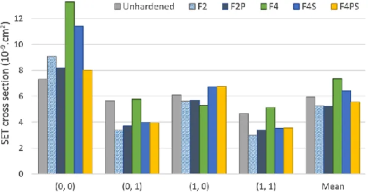
However, the asymmetric circuits are less effective when considering low LET particles as also shown in Fig. 13. Also, when adopting the asymmetric designs, not only the worst-case input SET cross-section is affected as can be seen in Fig. 14 in which the SET cross-section
σ
SET for each input signal and themean value are shown for the NOR gate. Due to a small increase in the cross-section for the inputs (0, 1), (1,0) and (1, 1), the mean SET cross-section reduction for the F2P and F4PS circuits are 1% and 13%, respectively. These results reaffirm the importance of considering input dependence when hardening digital logic circuits. The impact of adopting asymmetric designs is also evaluated under voltage variability and analyzed on the in-orbit SET rates.
C. Voltage Fluctuation
In addition to radiation effects, electronic circuits are susceptible to dynamic environmental variability, such as voltage fluctuations due to voltage drop and current derivative
di/dt noise [24]. Previous works have shown that voltage
variability reduces the reliability of circuits, especially when considering harsh environments under radiation effects [25,
26]. In [25], voltage variability has shown to reduce the threshold LET of different XOR topologies in FinFET and Trigate devices. Also, a reduction in the electrical masking capability of the gates and increase in the SET pulse width is observed in [26]. The IR drops due to the parasitic resistance of the power grids can lead to ±10% variation on the supply voltage. Accordingly, all circuits were analyzed considering a voltage drop of -10% of the nominal supply voltage of the technology, i.e. 0.12V. The SET cross-section and the variation ∆
σ
SET (in %) are shown for each circuit in Fig. 15. As expected,a reduction on the supply voltage of the circuits reduces the driving capability and consequently reduces the recovery efficiency, leading to a higher
σ
SET. The usage of diffusionsplitting technique induces insignificant impact on the circuit robustness to voltage variability as similar SET cross sections are obtained for the F4 and F4S circuits. However, for the 3 logic gates (inverter, NAND and NOR), the F4 and F4S circuits showed the greatest
σ
SET increase, ranging from 50% to 70%.Thus, as the number of fingers is increased, the circuit becomes more sensitive to the voltage drops. However, the asymmetric designs have shown to reduce the impact of voltage variability on the SET cross sections.
Considering only the inverter designs, the F4S circuit shows the lowest
σ
SET at nominal voltage but it is the most sensitive tovoltage drops, along with the F4 circuit. On the other hand, the F2 circuit provides the lowest
σ
SET at -10% of the supplyvoltage, and also the lowest variation on
σ
SET.For the NAND gate, the F4 circuit provides the lowest
σ
SET atnominal voltage, but it increases up to 66% with 10% reduction on the supply voltage. In this case, the unhardened circuit is the least sensitive design to voltage variation, leading to approximately 24% of increase in the
σ
SET. However, undervoltage drop, the lowest
σ
SET is still observed for theasymmetric design F4NS circuit. Compared to the unhardened
Fig. 14. SET cross section for the NOR designs at LET = 78.23 MeV.cm2/mg
for each input signal and the mean value.
Fig. 15. SET cross section considering a voltage drop of 10% over the nominal supply voltage and a particle LET of 5 MeV.cm2/mg. The percentage increase
NAND circuit, when the voltage fluctuation is considered, the F4NS reduced the
σ
SET up to 35%.For the NOR gate, similarly to the NAND gate, the F4 circuit provides the lowest
σ
SET at nominal voltage, but high sensitivityto the voltage drops, resulting in approximately 49% increase in the
σ
SET. However, it still provides the lowestσ
SET duringvoltage fluctuation. The diffusion splitting used in F4S increased its cross-section, but it still provides a lower
σ
SET thanthe F2 circuit, with the same area overhead.
D. Prediction of in-orbit SET rates
Based on the SET cross-section curves calculated with the current database provided by MC-Oracle, the in-orbit SET rates were estimated for the Low-Earth Orbit (LEO) and International Space Station (ISS) orbits with the OMERE software. OMERE is a tool dedicated to the analysis of space environment and radiation effects on electronics developed by TRAD and CNES [17]. The Integral Rectangular Parallelepiped (IRPP) approach is used to predict the SET rate, i.e. it is calculated by the convolution of the heavy-ion cross section data with the particle flux in the aforementioned orbits. This approach is a standard method specified by the European Cooperation for Space Standardization (ECSS) [27]. The NASA AP8MIN trapped radiation model is used for the proton fluxes under solar minimum conditions [28]. For the Galactic Comic Rays (GCR) fluxes, the international standard ISO 15390 model is used [29]. A fixed shielding of 1 g/cm2 is
considered. The calculated heavy-ions SET rates are shown in Fig. 16. Firstly, it can be noticed that all folded designs exhibit lower rates than its unhardened version (F0 circuit) for both orbits. In the case of the inverter, the F4S circuit provides the lowest rate with a reduction of approximately 82% and 77% in the ISS and LEO orbit, respectively. Similarly, for the NOR gate, the F4S showed the lowest SET rate. The folded transistor and diffusion splitting provided about 66% and 55% of reduction on the SET rate for the ISS and LEO orbit, respectively.
On the other hand, the F2 circuit is expected to have a lower rate for the NAND gate. Although the cross-section calculations were performed for heavy ions, the protons are expected to dominate the SEE rates in the LEO and ISS orbits. Due to its improved accuracy when compared to analytical models, the METIS method [18, 30, 31] was used to predict the proton-induced SET cross section curves from the heavy ions data. The sum of the SET rate induced by heavy ions and protons are
shown in Fig. 17. As expected, the overall SET rate increased considerably. However, in this case, the F4 and F4S circuits are no longer the most hardened designs. The F2 circuits have shown the lowest rate for the inverter and NAND gate, for both orbits. For the NOR gate, the asymmetric design F2P provided the lowest rate, about 10% reduction for the two orbits. Except for the F2N, one can notice that whenever the asymmetric design approach is adopted, a reduction on the overall SET rate is observed.
E. Transistor Scaling and Angular Dependence
With the increasing demand of better performance and low power in critical systems, advanced technology nodes have been studied to be employed in future missions. Due to the scaling of transistors, the hardening efficiency of these techniques might be reduced as the charge sharing effects are increased in response to the close proximity of the collecting zones in the advanced technology nodes. However, in FinFET technologies, the three-dimensional structure of the transistor impacts on the charge collection process and a reduction on the charge sharing effects might be expected as shown in [32]. Further, if an SOI technology is adopted, the hardening efficiency would be highly improved due to the lack of the diffusion contribution in the charge collection [33].
Concerning the angular effect in the charge collection, folded transistors have shown a low angle dependence as investigated in [34]. In fact, only the NMOS transistors have shown an increase in the total collected charge. For the worst-case scenario, in which the particle strikes the center of the drain area with a tilt angle of 60°, the total collected charge of a 4-finger NMOS transistor can be 20% higher than the collected charge in original design, without transistor folding. Thus, a very weak angle dependence can be expected in the SET cross-section of the folded designs, especially for low LET due to the reduced charge sharing. Further, according to [35], deeply scaled CMOS technologies present a marginal difference on the overall charge sharing effect between normal and angled strikes.
V. CONCLUSIONS
Physical layout design influences the main SEE mechanisms in VLSI circuits. Accordingly, RHBD techniques can be adopted at layout level. This work has analyzed the efficiency of transistor folding layout in improving the SET immunity of
Fig. 16. Heavy-ions SET rate estimated with OMERE [17] for each circuit and its hardened version considering the LEO (800km, 98°) and ISS (400km, 51.64°) orbit. The SET cross section average of each input signal is used.
Fig. 17. Total SET rate estimated with OMERE [17] for each circuit and its hardened version for the LEO (800km, 98°) and ISS (400km, 51.64°) orbit considering heavy ions and protons. Proton-induced SET rates are estimated with the METIS method [18, 19]. The SET cross section average of each input signal is used.
8
digital circuits. In addition to the higher threshold LET, the results show that folded designs can provide lower SET cross-section, especially at low LET. The number of fingers were also explored. For LET lower than 10 MeV.cm2/mg, the hardening
efficiency of the folded designs increases as the number of fingers is increased. However, at high LET, the 2-finger designs showed the best performances. Increasing the number of fingers increases greatly the final layout area. Thus, a layout technique was proposed to overcome the area overhead of multiple-finger designs. In the diffusion splitting approach, the active diffusion is split into two strips and placed vertically aligned within each other. Besides reducing the layout area, diffusion splitting may also improve the SET cross-section depending on the circuit topology, input signal and ion LET. Due to the strong input dependence of these techniques, it was also proposed to adopt asymmetric designs, i.e. applying the hardening techniques only in the PMOS or NMOS devices, depending on the worst-case input scenario of the logic gate. Voltage variability was also explored due to its impact on the reliability of deeply scaled technologies. The folded designs have shown a higher sensitivity to voltage fluctuation. However, the usage of asymmetric design showed to reduce it. And, lastly, the in-orbit SET rates were predicted for the LEO and ISS orbits. When the SET rate is only calculated for heavy ions, all the folded designs provided lower rate than the unfolded designs. However, the protons dominate the SEE rates in the LEO and ISS orbits. When protons are taken into account, the 2-finger designs (symmetric and asymmetric) and the asymmetric 4-finger design with DS are the most hardened circuits.
REFERENCES
[1] V. Ferlet-Cavrois, L. W. Massengill, and P. Gouker, “Single Event Transients in digital CMOS – A review,” IEEE Trans. Nucl. Sci., vol. 60, no. 3, pp 1767-1790, Jun 2013.
[2] P. E. Dodd, M. R. Shaneyfelt, J. R. Schwank, and J. A. Felix, “Current and future challenges in radiation effects on CMOS electronics,” IEEE
Trans. Nucl. Sci., vol. 57, no. 4, pp 1747-1763, Aug. 2010.
[3] G. Hubert, L. Artola and D. Regis, “Impact of Scaling on the soft error sensitivity of bulk, FDSOI and FinFET technologies due to atmospheric radiation,” Integration, the VLSI Journal, vol. 50, pp 39-47, Jan. 2015. [4] R. C. Lacoe, “Improving integrated circuit performance through the
application of hardness-by-design methodology,” IEEE Trans. Nucl. Sci., vol. 55, no. 4, pp. 1903-1925, Aug. 2008.
[5] K. Lilja, M. Bounasser, S.-J. Wen, R. Wong, J. Holst, N. Gaspard, et al., “Single-event performance and layout optimization of flip-flops in a 28-nm bulk technology,” IEEE Trans. Nucl. Sci., vol. 60, no. 4, pp. 2782-2788, Aug. 2013.
[6] W. Zhao, C. He, W. Chen, R. Chen, P. Cong. F. Zhang, et al., “Single-event multiple transients in guard-ring hardened inverter chains of different layout designs,” Microelectronics Reliability vol. 87, pp. 151-157, Aug. 2018.
[7] R. C. Lacoe, J. V. Osborn, R. Koga, S. Brown, D. C. Mayer, “Application of hardness-by-design methodology to radiation-tolerant ASIC technologies,” IEEE Trans. Nucl. Sci., vol. 47, no. 6, pp. 2334-2341, Dec. 2000.
[8] G. Anelli, M. Campbell, M. Delmastro, F. Faccio, S. Floria, A. Giraldo,
et al., “Radiation tolerant VLSI circuits in standard deep submicron
CMOS technologies for the LHC experiments: practical design aspects,”
IEEE Trans. Nucl. Sci., vol. 46, no. 6, pp. 1690-1696, Dec.1999.
[9] J. Chen, S. Chen, Y. He, J. Qin, B. Liang, B. Liu, and P. Huang, “Novel layout technique for single-event transient mitigation using dummy transistor,” IEEE Trans. Dev. Mat. Reliab., vol. 13, no. 1, pp. 177-184, Mar. 2013.
[10] J. D. Black, P. E. Dodd, and K. M. Warren, “Physics of multiple-node charge collection and impacts on single-event characterization and soft
error rate prediction,” IEEE Trans. Nucl. Sci., vol. 60, no. 3, pp. 1836-1851, Jun. 2013.
[11] F. L. Kastensmidt, T. Assis, I. Ribeiro, G. Wirth, L. Brusamarello, and R. Reis, “Transistor sizing and folding techniques for radiation hardening,” in Proc. RADECS, Bruges, Belgium, 2009, pp. 512-519.
[12] Y. Chi, R. Song, S. Shi, B. Liu, L. Cai, C. Hu, and G. Guo, “Characterization of single-event transient pulse broadening effect in 65 nm bulk inverter chains using heavy ion microbeam,” IEEE Trans. Nucl.
Sci., vol. 64, no. 1, pp. 119-124, Jan. 2017.
[13] J. A. Maharrey, “Characterization of Heavy-Ion Induced Single Event Transients in 32nm and 45nm Silicon-on-Insulator Technologies,” M.S. thesis, Vanderbilt University, Nashville, Tennessee, 2014.
[14] T. W. Her and D. F. Wong, “Cell area minimization by transistor folding,” in Proc. Euro-DAC, Hamburg, Germany, 1993, pp. 172-177.
[15] F. Wrobel and F. Saigné, “MC-Oracle: a tool for predicting Soft Error Rate,” Computer Phys. Comm., vol. 182, pp. 317 – 321, Elsevier, 2011. [16] Y. Q. Aguiar, F. Wrobel, J.-L. Autran, P. Leroux, F. Saigné, A. D.
Touboul, and V. Pouget, “Impact of Complex-Logic Cell Layout on the Single-Event Transient Sensitivity,” IEEE Trans. Nucl. Sci., vol. 66, no. 7, pp. 1465-1472, Jul. 2019.
[17] The OMERE 5.3 Software by TRAD and CNES. Available online: http://www.trad.fr/en/space/omere-software (accessed on 10 October 2019)
[18] C. Weulersse, F. Wrobel, F. Miller, T. Carrière, R. Gaillard, J.-R. Vaillé,
et al., “A Monte-Carlo Engineer Tool for the Prediction of SEU Proton
Cross Section from Heavy Ion Data,” in Proc. RADECS, Sevilla, Spain, 2011, pp. 376-383.
[19] C. Weulersse, F. Miller, T. Carrière, and R. Mangeret, “Prediction of proton cross sections for SEU in SRAMs and SDRAMs using the METIS engineer tool,” Microelectronics Reliability, vol. 55, no. 9-10, pp. 1491-1495, Sept. 2015.
[20] F. Wrobel, L. Dilillo, A. D. Touboul, V. Pouget, F. Saigné, “Determining Realistic Parameters for the Double Exponential Law that Models Transient Current Pulses,” IEEE Trans. Nucl. Sci., vol. 61, no. 4, pp. 1813-1818, Aug. 2014.
[21] Y. Q. Aguiar, F. Wrobel, J.-L. Autran, P. Leroux, F. Saigné, A. D. Touboul, and V. Pouget, “Analysis of the charge sharing effect in the SET sensitivity of bulk 45 nm standard cell layouts under heavy ions,”
Microelectronics Reliability, vol. 88-90, pp. 920-924, Sept. 2018.
[22] Y. Q. Aguiar, F. Wrobel, J.-L. Autran, P. Leroux, F. Saigné, A. D. Touboul, and V. Pouget, “Radiation Hardening Efficiency of Gate Sizing and Transistor Stacking based on Standard Cells,” Microelectronics
Reliability, vol. 100-101, pp. 1-5, Sept. 2019.
[23] Y. Q. Aguiar, F. Wrobel, J.-L. Autran, P. Leroux, F. Saigné, V. Pouget, and A. D. Touboul, “Mitigation and Predictive Assessment of SET Immunity of Digital Logic Circuits for Space Missions,” Aerospace, vol. 7, no. 2, pp. 12-26, Feb. 2020.
[24] S. Bokar, T. Karnik, S. Narendra, J. Tschanz, A. Keshavarzi, and V. De, “Parameter variations and impact on circuits and microarchitecture,” in
Proc. DAC, Anaheim, CA, USA, 2003, pp. 338-342.
[25] Y. Q. Aguiar, C. Meinhardt, and R. Reis, “Radiation sensitivity of XOR topologies in multigate technologies under voltage variability,” in Proc.
IEEE LASCAS, Bariloche, Argentina, 2017, pp. 1-4. 10.1109/LASCAS.2017.7948075
[26] S. A. Olowogemo, W. H. Robinson and D. B. Limbrick, “Effects of Voltage and Temperature Variations on the Electrical Masking Capability of sub-65nm Combinational Logic Circuits,” in Proc. IEEE DFT, Chicago, USA, 2018, pp. 1-6.
[27] ECSS-E-HB-10-12A (2010) Space Engineering: Calculation of radiation and its effects and margin policy handbook. 17 Dec.
[28] D. M. Sawyer and J. I. Vette, “AP-8 trapped proton environment for solar maximum and solar minimum,” NASA TM-X-72605, 1976.
[29] ISO 15390, "Space environment (natural and artificial)-Galactic cosmic ray model", 2004.
[30] C. Weulersse, S. Morand, F. Miller, T. Carrière, and R. Mangeret, “Simulation of Proton Induced SET in Linear Devices and Assessment of Sensitive Thicknesses,” in Proc. RADECS, Moscow, Russia, 2015, pp. 1-4.
[31] C. Weulersse, S. Morand, F. Miller, T. Carrière, and R. Mangeret, “Predictions of Proton Cross-Section and Sensitive Thickness for Analog Single-Event Transients,” IEEE Trans. Nucl. Sci., vol. 63, no. 4, pp 2201-2207, Aug. 2016.
[32] Y.-P. Fang and A. S. Oates, “Neutron-Induced Charge Collection Simulation of Bulk FinFET SRAMs Compared With Conventional Planar
SRAM,” IEEE Trans. Dev. Mat. Reliab., vol. 11, no. 4, pp. 551-554, Dec. 2011.
[33] F. El-Mamouni, E. X. Zhang, D. R. Ball, B. Sierawski, M. P. King, R. D. Schrimpf, et. al. “Heavy-ion-induced current transients in bulk and SOI FinFETs,” IEEE Trans. Nucl. Sci., vol. 59, no. 6, pp. 2674–2681, Dec. 2012.
[34] N. M. Atkinson, “Single-Event Characterization of a 90-nm bulk CMOS digital cell library,” Master Thesis, Vanderbilt University, USA, 2010. [35] J. Ahlbin, M. J. Gadlage, D. R. Ball, A. W. Witulski, B. L. Bhuva, R. A.
Reed, et al., “The Effect of Layout Topology on Single-Event Transient Pulse Quenching in a 65 nm Bulk CMOS Process,” IEEE Trans. Nucl.
![Fig. 17. Total SET rate estimated with OMERE [17] for each circuit and its hardened version for the LEO (800km, 98°) and ISS (400km, 51.64°) orbit considering heavy ions and protons](https://thumb-eu.123doks.com/thumbv2/123doknet/14666408.740917/8.918.477.845.248.433/total-estimated-omere-circuit-hardened-version-considering-protons.webp)
