HAL Id: hal-01745351
https://hal.archives-ouvertes.fr/hal-01745351
Submitted on 28 Mar 2018
HAL is a multi-disciplinary open access
archive for the deposit and dissemination of
sci-entific research documents, whether they are
pub-lished or not. The documents may come from
teaching and research institutions in France or
abroad, or from public or private research centers.
L’archive ouverte pluridisciplinaire HAL, est
destinée au dépôt et à la diffusion de documents
scientifiques de niveau recherche, publiés ou non,
émanant des établissements d’enseignement et de
recherche français ou étrangers, des laboratoires
publics ou privés.
Crossbar architecture based on 2R complementary
resistive switching memory cell
Weisheng Zhao, Y Zhang, Jacques-Olivier Klein, Damien Querlioz, Dafine
Ravelosona, Claude Chappert, Jean-Michel Portal, Marc Bocquet, Hassen
Aziza, Damien Deleruyelle, et al.
To cite this version:
Weisheng Zhao, Y Zhang, Jacques-Olivier Klein, Damien Querlioz, Dafine Ravelosona, et al..
Cross-bar architecture based on 2R complementary resistive switching memory cell. 2012 IEEE/ACM
International Symposium on Nanoscale Architectures , Jul 2012, Amsterdam, Netherlands.
�10.1145/2765491.2765508�. �hal-01745351�
Crossbar Architecture Based on 2R Complementary
Resistive Switching Memory Cell
W.S. Zhao, Y.Zhang, J.O Klein, D. Querlioz, D.
Ravelosona, C. Chappert
IEF, Univ. Paris-Sud, - UMR8622, CNRS, Orsay, France [email protected]
J.M. Portal, M. Bocquet, H. Aziza, D.Deleruyelle, C.
Muller
Aix-Marseille University, IM2NP – UMR CNRS 7334 Marseille, France
Abstract—Emerging non-volatile memoires (e.g. STT-MRAM, OxRRAM and CBRAM) based on resistive switching are under intense R&D investigation by both academics and industries. They provide high performance such as fast write/read speed, low power and good endurance (e.g. >1012) beyond Flash
memories. However the conventional access architecture based on 1 transistor + 1 memory cell limits its storage density as the selection transistor should be large enough to ensure enough current for the switching operation. This paper describes a design of crossbar architecture based on 2R complementary resistive switching memory cell. This architecture allows fewer selection transistors, and minimum contacts between memory cells and CMOS control circuits. The complementary cell and parallel data sensing mitigate the impact of sneak currents in the crossbar architecture. We performed transient simulations based on two memory technologies: STT-MRAM and OxRRAM to validate the functionality of this design by using CMOS 65 nm design kit and memory compact models.
Keywords-Crossbar; Resistive Switching; complementary cell;
I. INTRODUCTION
Modern computing systems suffer from rising static power due to the high leakage currents, which increase exponentially following the fabrication node miniaturization of CMOS technology (e.g. <90 nm) [1]. According to ITRS 2011, the static power will start to play the major role of whole power consumption in the next years [2]. In order to relieve this power issue, emerging non-volatile memoires (NVM) based on resistive switching are under intense R&D investigation by both academics and industries. Spin transfer torque magnetic random access memory (STT-MRAM) [3]; Conductive-Bridge RAM (CBRAM) [A-4] and Oxide Resistive RAM (OxR-RAM) [A-5] are among the most promising technologies. They promise to provide much higher performances than Flash memory such as fast write/read speed, low power and good endurance (e.g. >1012). Since 2009, a number of NVM
pre-industrial prototypes [6-10] were presented and the commercial products should be available soon.
Even though these emerging NVM are based on different physics, they hold many common features. For instance, they are two terminal nanoscale devices; their resistances vary to present ‘0’ and ‘1’; their memory cell are implemented at back-end of line (BEOL) process [A-6-10] etc. Thereby they use the
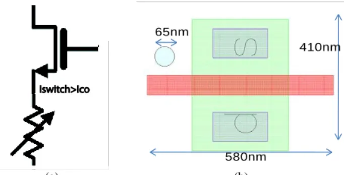
same access structure 1T (transistor)+ 1R (resistive memory) shown in Fig.1a, and then benefit the existing peripheral control circuits of Dynamic RAM (DRAM). However this structure presents some drawbacks: the transistor is normally much larger than the minimum size in order to obtain the sufficient current for fast memory cell switching; there are lots of large interconnects between CMOS circuits and memory cell due to the thick metals (e.g. M3). They make the density of these NVM technologies lower than Flash memory. For example, Fig.2b shows the 65 nm layout implementation of the conventional STT-MRAM access design. In order to get fast switching speed (e.g. 10 ns), the selection transistor should be large enough to ensure a high current (e.g. 100 A). The CMOS circuits impose definitively the density of STT-MRAM density instead of magnetic tunnel junction (MTJ) [A-11].
(a) (b)
Figure 1. Conventional access approach based on 1Transistor and 1 resistive memory cell. (a) Circuit diagram (b) Layout implementation at 65 nm; the size of selection transistor is about 56 F2.
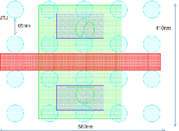
Crossbar architectures were proposed to relax the density limitation of two-terminal resistive switching devices imposed by the CMOS [A-8-11]. There are only interconnects between CMOS circuits and memory cell on the edge of the crossbar array. A number of memory cells share the same selection transistor (see Fig.2). The cell area efficiency can be greatly improved, and the back-end process of NVM defines then the density instead of CMOS circuits. However, the conventional crossbar architectures suffer from sneak currents and low data access speed. The former is the most critical as the data sensing can be disturbed completely by the sneak currents. Moreover, there are parasite resistances throughout a
large-65nm
580nm
scale crossbar array, which leads to lots of sensing errors [A-6-12]. These issues are difficult to surmount and few efficient design solutions addressing this issue have been reported previously in the literature. In this paper, we present a new crossbar architecture based on complementary resistive switching memory. Combining with parallel data sensing, the impact of sneak currents and parasite resistance can be mitigated to ensure the correct data sensing. In order to validate the functionality of this design, we performed transient simulations based on two memory technologies: STT-MRAM and OxRRAM by using CMOS 65 nm design kit and memory compact models.
Figure 2. The layout implementation promises the best area efficiency, where the die area per storage bit is 2F2 and the selection transistor is shared
by a number of MTJs associated in the same word (e.g. 4).
The rest of the paper is organized as follows. In the next section, we introduce the principles of STT-MRAM and OxR-RAM. In Sections III, we describe the design details of complementary crossbar architecture. In Sections IV, we show the transient simulation of the crossbar architecture by using CMOS 65 nm design kit and compact models of the STT-MRAM and OxR-RAM. Finally, a discussion and concluding remarks are provided in section V.
II. EMERGING RESISTIVE SWITCHING MEMORIES
In this section, we introduce briefly the principles of STT-MRAM and OxR-RAM, which were studied as resistive switching memory cell in the proposed crossbar architecture.
A. STT-MRAM technology principle
Magnetic RAM (MRAM) promises stable non-volatility, fast write/read access speed and infinite endurance etc [A-2-3]. The MRAM storage element, MTJ nanopillar is mainly composed of three thin films: a thin oxide barrier and two ferromagnetic (FM) layers (see Fig.3a). As a result of the tunnel magnetoresistance (TMR) effect [A-12], the nanopillar resistance, RP or RAP, depends on the relative orientation,
Parallel (P) or Anti-Parallel (AP), of the magnetization of the two FM layers. By using crystalline MgO barriers, the TMR ratio=RAP-RP/RP of MTJ nanopillars can reach more than
600% at room temperature [A-13-14]. This allows the state of
MTJs to be detected easily by CMOS sense amplifiers [A-15]. Spin transfer torque (STT) is one of the most promising switching approaches thanks to its high power efficiency and fast writing speed [A-4-5, 16]. This switching mechanism greatly simplifies the CMOS switching circuit, as only a bi-directional current is required. One time the current through the MTJ exceeds the critical current; the MTJ will switch its state (see Fig.3b). It opens the door to build up the first true universal memory with MRAM, which should provide both large capacity (> Gigabit) and high speed (<ns). Recent progress demonstrate perpendicular magnetic anisotropy (PMA) in CoFeB/MgO structures provides a high energy barrier E to deal with the issue of thermal stability of in-plane anisotropy, which also presents the advantages of low threshold current, high speed operation and high TMR ratios comparing with in-plane anisotropy.
(a) (b)
Figure 3. (a) Vertical structure of an MTJ nanopillar composed of CoFeB/MgO/CoFeB thin films. (b) Spin transfer torque switching mechanism: the MTJ state changes from parallel (P) to anti-parallel (AP) as the positive electron flow direction IP->AP>IC0, on the contrast, its state will
return as the negative electron flow direction IAP->P>IC0.
B. OxRRAM technology principle
A large number of oxide-based materials showing a resistive switching are reported in the literature [Waser07] [Seo04] [Kim10]. Among them, metal oxides like HfO2, Ta2O5,
NiO, TiO2 or Cu2O are promising candidates due their
compatibility with CMOS processes and high on/off resistance ratio. In its simplest form, resistive memory element relies on a Metal/Insulator/Metal (MIM) stack (Fig. 4) that can be easily integrated into Back-End Of Line (BEOL).
The MIM structure is generally composed of an active layer, usually a non-stoechiometric dielectric. The bipolar behavior is mainly due to an asymmetrical geometry of the electrode. In recent years, many studies have highlighted the good performances of non-stoichiometric HfOx [Lee08-IEDM]
films used as switching layer (also used in memristors demonstrated by Hewlett-Packard [Lee10]). Besides, an additional buffer layer, also called interface layer, such as Al2O3 or Ti may play an important role in the reliability and the
reduction of the programming voltage [Lee08-IEDM] [Lee10]. OxRRAM technology is still in its “infancy” since the physics of resistance switching is not yet fully understood. So far, it is broadly accepted that the electro migration of oxygen vacancies plays a critical role in the resistance switching [Ahnl07]. Si/SiO 2 CoFeB MgO CoFeB Ta Ru Cr/Au Ta Ru Ta Al2O3 Al2O3 V- V+ CoFeB MgO CoFeB P P AP AP IP ->AP >IC0 IAP ->P >IC0 CoFeB MgO CoFeB CoFeB MgO CoFeB CoFeB MgO CoFeB
Figure 4. OxRRAM memory element stack overview.
Figure 5. Typical I-V characteristic of a bipolar OxRRAM memory device.
After an initial electroforming process, the memory element may be reversibly switched between reset (high resistance) and set states (low resistance). Electroforming stage corresponds to a voltage-induced resistance switching from an initial very high resistance state (virgin state) to a conductive state. In the literature, unipolar, bipolar and non-polar electrical behaviors are reported. In the case of bipolar switching, addressed in this paper, bipolar voltage sweeps are required to switch the memory element (Fig. 5). Resistive switching in an OxRRAM element corresponds to an abrupt change between a High Resistance State (RHRS or OFF state) and a Low Resistance
State (RLRS or ON state). This resistance change is achieved by
applying specific threshold voltage to the structure (i.e. VSET
and VRESET).
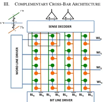
III. COMPLEMENTARY CROSS-BAR ARCHITECTURE
The cross point architecture is shown in Fig.6, which is composed of three parts: a memory array for data storage, bit line and word line drivers, read decoder and sense amplifiers for read operation. The operating mechanisms will be detailed in the following subsections:
A. Cell structure and operation
Every cell is composed of two resistive switching elements (2R) as shown in inset of Fig.6. For every cross-point, a common word line (WL) is connected to the bottom electrode (BE) of both resistive switching elements while their top electrode (TE) are respectively connected to bit-line (BL) and complementary bit-line (
BL
). Cell programming operation are performed in two phases, as follow: 1st Phase: For the selected word, the common WL is
grounded and all the bit-line and complementary bit-line are biased to VDD and a current flow from top to bottom
electrode, to set the resistive elements to a low resistance state (RLRS) as shown Fig.7.a.
2nd Phase: For the selected word, the common WL is set to
VDD while BL and
BL
are biased to complementary valuein order to selectively reset (high resistance state – RHRS)
either the top resistive element or the bottom resistive element. In this case the current flows from the bottom to the top electrode. At the end of the programming operation both elements have opposite resistance state. Fig.7.b.
All unselected word-line and bit-line are biased to VDD/2
to keep resistive elements unchanged. As shown Fig.7.c two sub-array conditions are found for the unselected cells. One sub-array that share bit-line or word-line with the selected word see a biasing of VDD/2 and all the other cells
see a biasing of 0 volt.
Metal IL active materials: TiOx, Ta2O5, HfO2 Metal TE BE Memory cell ! " #$%&' ()*' + (, " #$(-%. &' /( 0 1--' .$ () 12 ($ "( 3 2 (-%. &' /( !456( !754( 78 9 ( 78 : : (
Figure. 6: Proposed Cross Point architecture (4 × 2 words array with 2 bits word length). It includes three parts, a cross-point array of 2R cell for data storage, word line (left side) and bit line (bottom) driver and read circuits (top).
+ - +
-SENSE DECODER
BIT LINE DRIVER
W O R D LI N E D R IV ER WL0 WL1 WL2 WL3 BL0 BL1 BL2 BL3 BL0 BL1 BL2 BL3 ! "# ! "# $ "# ! "# ! "# $"# $"#
The read operation is performed through a differential sensing of the bit-line and complementary bit-line and will be described in the sense-amplifier sub-section.
Figure. 7. Operation process in the cross point array: (a) For the selected word, the WL=gnd and both bit-line are biased to VDD (write 1st phase). (b) For
the selected word, WL=VDD while the bit-line are set to opposite values (write
2nd phase). (c) For the unselected words, both the word-lines and the bit-lines
are biased to VDD/2 to ensure that unselected resistive elements do not set or
reset.
B. Array architecture
As shown in Fig.6, the array is divided in M word per word line (e.g. 2). Each word is composed of N bits (e.g. 2). There is one driver circuit associated with each word-line and bit-line to ensure the proper biasing conditions for all modes of operations (write, read, unselected). A read decoder connects the N sense-amplifier to the selected word during the read phase.
C. Driver circuit
When dealing with bipolar resistive switching element, one may be able to apply bipolar voltage between the top and bottom electrode as well as bidirectional current to properly achieved programming phase. Moreover, as described in previous sub-section, voltage and current must remain below threshold to do not changed resistance value of unselected cell. To achieve this set of conditions, drivers have to be connected to the bit-line and the word-line. Row & column decoders together with the control logic activate the drivers. Decoder and control logic are similar to other well-known memory circuits and are not described here. A driver is composed (Fig.8) of one PMOS to connect a line to VDD and two NMOS
to connect a line to gnd or VDD/2. It is important to note that the
driver sizing is crucial to control the current and voltage levels
applied to the cell, which is a mandatory step to properly determine the RHRS and RLRS values.
Figure. 8. Bit-line and word-line driver description. Two NMOS and one PMOS are connected to each bit-line and word-line to ensure correct biasing during all phases of operation (Write 1st and 2nd phase, Read 1st and 2nd phase).
D. Sense amplifier definition
The read operation of data stored in cross-point resistive switching memory is currently one of the major challenges to develop this approach. Indeed, sneak path or destructive read with CRS element [S Tappertzhofen11] are a strong limit to develop this type of architecture. Moreover, the resistance ratio (RHRS/RLRS) and the process variations have to be
considered when designing a sense solution. A sense amplifier performing with high reliability is then required. Fig.9 shows a pre-charge based sense amplifier (PCSA), which has demonstrated the best tolerance to different sources of variation [A-13], while keeping high speed and low power. In this SA, the read operation is performed in two phases:
!" "# $%&# !" "# !"! #$ !"! #$ $%&# !" "# !" "# !%! #$ !"! #$ ' ()*+# ,- .#/ 012+# ' ()*+# 34 "#/ 012+#56789# !"#$ !%#$ ! "#$ ! "%$ ! "&$ ! "'$ ( "#$ ( "%$ ( "&$ ( "'$ ( "#$ ( "%$ ( "&$ ( "'$ ! " #" $%" &'( ) *&' +! 123$4*$14%', ,-. '/+0' 5'/+0' ! 123$4*$14%' /$0' +, ,-. '/+0' ! 123$4*$14%' BLi BLi WLi VDD gnd VDD/2 VDD gnd VDD gnd VDD/2 VDD/2 Write 2ndPhase Write 1stPhase Read 2ndPhase Unselected Unselected Unselected Write 1stPhase Write 2ndPhase Write 2ndPhase Write 1stPhase Write 2ndPhase Write 2ndPhase
Figure. 9: Pre-Charged Sense Amplifier (PCSA) for data sensing: MPC0 and
MPC1 serve to pre-charge the bit-line to VDD; MPA0, MPA1, MNA0 and MNA1
constitute the amplifier; MNE0 and MNE1 play the role of “Enable”. BL BL WL SEN PCH PCH RHRS RLRS Q Q MPC0 MPA0 MPA1 MPC1 MNA0 MNA1 MNE0 MNE1
1st Phase: The SA is first connected to the bit-line of the
selected word with SEN set to ‘1’ and the circuit is pre-charged with PCH equals ‘0’.
2nd Phase: The data stored in the 2R cell can be evaluated to
logic level at the output Q as PCH is changed to ‘1’ and WL is pulled down to ‘0’.
E. Sneak current mitigation
As mentioned previously, this structure is designed to mitigate the impact of sneak currents and parasite resistance. Thanks to the complementary configuration in the memory cell, there are always the same numbers of unselected transistors and the same distance of wire connection (see Fig.7), this balanced structure allows the impact of parasite resistance to be neglected during data sensing.
(a)
(b)
Figure. 10. (a) The comparison of expected current value, sensing current in series and sensing current in parallel VS the ROFF/RON ratio (b) Parallel sensing
currents to address ROFF and RON in the crossbar array, the sneak currents in
unaddressed RON memory cell VS the ROFF/RON ratio.
Parallel data sensing allows the impact of sneak currents to be mitigated as all the bit lines are set to the same voltage potential. We performed a simple simulation of 4×4 crossbar
array and evaluated the impact of sneak currents on data sensing for different architectures. The worst case is implemented, where the cell to address is ROFF and all the
other cells are RON. The sensing of this cell suffers from the
most important impact of sneak current. RON is fixed to 10K
ohm; the parasite resistance in each wire (BLs and WLs) connected is set to 10 ohm. Fig.10a shows that the current value for sensing in series (black square curve) is much higher than the expected current value (red point curve). This confirms that the sneak currents can perturb completely the sensing operation if there are no any mitigation solutions. However, the current value for sensing in parallel (blue triangle curve) equals nearly to the expected current value as the ROFF/RON is lower than 10. This can be explained by the
reduction of sneak currents in each memory cell (blue square curve) and the decreasing of sensing current difference between ROFF and RON, as shown in Fig.10b.
IV. VALIDATION WITH BIPOLAR OXRRAM AND
STT-MRAMMEMORY CELL
The aim of this section is to present the architecture validation with array simulation on both NVM technologies by using compact models and CMOS 65 nm design kit. In the following, we describe briefly the compact models. Transient simulation of the proposed architecture with STT-MRAM and OxRRAM are then presented.
A. Resistive Memory Cell modeling 1) STT-MRAM compact model
A CoFeB/MgO/CoFeB STT-MTJ compact model has been recently developed based on the physical theories and experimental measurements of perpendicular magnetic anisotropy (PMA) MTJ [A-16]. It integrates the physical models of static, dynamic and stochastic behaviors. The major parameters are shown in the Table.I.
The static behaviors of STT switching in PMA MTJ is mainly based on the calculation of threshold or critical current
Ic0, which can be expressed by the Eq.A-2 [A-17],
E g e V H M g e I B K S B c ( 0 ) 2 0
(A-2)
where E is the barrier energy (see also Eq.1), α is the magnetic damping constant, γ is the gyromagnetic ratio, e is the elementary charge, μB the Bohr magneton, V the volume of
the free layer and kB the Boltzmann constant.
The switching dynamics of STT in PMA MTJ is presented in [A-18] and Eq.A-3 shows the dependence of switching current Iwrite value with the duration.
) ( ) 1 ( ] ) 4 ln( 2 [ 1 0 2 I I P P em P C c write free ref ref B (A-3)
where C≈0.577 is the Euler’s constant, ξ=E/kBT the activation
energy in units of kBT, Pref, Pfree the tunneling spin
polarizations of the reference and free layers, we assume that Pref=Pfree=P for this compact model, m is the magnetic moment
of free layer.
Fig.11 shows the transient simulation of this compact model, which could also verify the agreement of the dynamic
10 100 1000 1 10 100 1000 Out pu t Cu rren t (uA) ROFF-RON/RON
Current (Sensing in series) Expected Sensing Current Current (Sensing in parallel)
10 100 1000 0,1 1 10 100 Output current (RON) Output current (ROFF) Sneak current ROFF-RON/RON O u tp u t C u rr e n t (u A ) 10 12 14 16 18 20 22 24 26 S n e a k C u rr e n t o n R ON ( n A )
behavior between physical models and experimental measurements. We found that the switching delay is inversely proportional to the writing current as described in Eq. A-3.
Figure.10. Transient simulation of the PMA MTJ demonstrates the integration of dynamic model and helps us to evaluate the tradeoff between CMOS die area and switching speed.
2) OxRRAM Compact Model
The proposed OxRRAM modeling approach relies on a physical model accounting for both set and reset operations in bipolar resistive switching devices. In considering electric field-induced migration of oxygen vacancies within the switching layer, the model enables continuously accounting for both set and reset operations into a single master equation in which the resistance is controlled by the diameter of the conduction pathways (): T k V q E a T k V q E a b c e ll b c e ll e e d t d m a x (1)
In equ. 1, represents the creation/destruction rate, Ea the activation energy and VCell the cell voltage. Based on this
expression, the cell current can be expressed as a function of the size of this conductor path:
LRS HRS HRS
Cell CellL
V
I
2
max2
4
(2)Where LRS andHRS represents the conductivity in the
Low Resistance State and the High Resistance State. This physical model demonstrates its flexibility to match the switching voltages, the levels current and the dynamics dependence on various technologies [NVMTS11][IDT11]. This last point is a key point to perform a realistic circuit analysis.
In this way, the model carte has been adjusted to fit at the behavior of the most aggressive component from literature: Set/Reset voltage below 1V [Cagli11-IEDM] and programming time around 10ns [Lee08-IEDM]. Table I summarizes the cell operation parameters for very short programming pulse.
TABLE I. CELL OPERATION PARAMETERS.
VTE (V) VBE (V) STATE
SET (Write) 0.8@10ns 0 ONOFF RESET (Erase) 0 -0.8V@10ns OFFON Read <0.4@10ns Sensing ON or OFF
B. Architecture simulation
The aim of this section is to validate the functionality of the architecture for both technologies
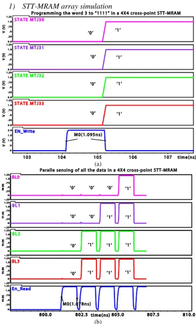
1) STT-MRAM array simulation
(a)
(b)
Fig. 11. (a) Configuration of the small crossbar array (b) Parallel sensing of a 4×4 cross-point array within ~5ns (~1.2ns/word).
Fig. 11 (a) and (b) demonstrate the mixed simulation of parallel writing /reading for this 4×4 cross-point resistive
TABLEI
PARAMETERS AND VARIABLES PRESENT IN THE FITTING FUNCTIONS
Parameter Description Default Value
Area MTJ surface 65 nm x 65 nm
TMR(0) TMR ratio with 0 Vbias 120%
V Volume of free layer surface x1.3 nm
R·A Resistance-area product 10 Ωµm2
Vwrite Writing voltage 1.5 V Vread Reading voltage 1.2 V
switching memory and confirm the expected operations shown in the section III. For instance, it takes only one cycle of switching duration, ~1.1 ns driven by the signal “EN_Write” to program a word to “0000” or “1111”. Thanks to the fast computing speed of the PMA MTJ compact model, the simulation of this 4×4 cross-point memory can be performed in ~30 minutes in a medium performance CAD server (two Xeon: 4-Core, 12MB cache, 2.4GHz and 8GB 1.3GHz RAM).
In order to keep the same data read access speed with that of data programming, the pulse duration of “En_Read” (see also Fig.6) is set to ~1.1ns. The word address changes between two “En_Read” pulses during ~100 ps and the data stored in this 4×4 cross-point STT-MRAM can be detected word by word in ~5ns. It is noteworthy that the sensing speed can be accelerated up to ~200 ps/word [20], which would lead to an asymmetric delay between the programming and reading operations. Nevertheless, this asymmetric delay is nearly ubiquitous in non-volatile memories and it may present some advantages in terms of power and access speed as the non-volatile memories are read more frequently than programmed.
2) OxRRAM array simulation
To validate the efficiency of the proposed architecture with the OxRRAM technology, an array composed of 32 word-lines of 2 words of 16 bits including line drivers and PCSAs, as shown Fig.11, is fully simulated. Moreover, as depicted in the inset Fig. 11, WL and BL resistance and capacitance are modeled through RC element distributed all over the array.
The simulation is divided in two: a write phase, where all the words in the array are successively written with the pattern given Fig.12, followed by the selective read of the top-left word in the array. The write time is set to 20ns with 10ns by phase. The read time is also set to 20ns with 10ns pre-charge and 10ns to generate a logic value on the output. It is important to note that the write and read timing value gives a strong
margin versus the capability of the PCSA, as depicted on simulation results given Fig.13.
The Fig.13 gives an overview of the simulation results, with the writing phase of: a cell in the selected word, a cell in an unselected word, a cell in a unselected bit-line and of a read phase.
The Fig.13(a) shows the behavior of the cell00 while in a
first phase the cell is programmed (cell both OxRRAM elements are set and only top OxRRAM element is reset). Moreover, this simulation results validates the fact that the cell00 remains unchanged, during the write phase of the second
word (word01) on the same word-line (WL0) or during the write
phase of the fisrt word (word10) of the second word-line (WL1) Figure. 13: Simulation results with (a) write phase of a selected cell, behavior of an unselected cells and read phase of Word00 (cell00 and cell01)
Figure. 12: Topologic representation of the pattern store in the array, yellow color stand for ‘0’ and green for ‘1’. The pattern used is a “checkerboard” per word. The reading phase targets the top-left word (word00) . Scrambling
aspects are not taken into account.
Set Reset Unchanged same WL Unchanged same BL IBOT ITOP VBL0 VBL0b VWL0 Precharge Read Cell00= ‘0’ Cell01= ‘1’ VWL0 VSEN VPCH 10ns 10ns
(a) Write phase of a selected cell, unselected cell (same WL, same BL)
(b) Read phase of word00(cell00, cell01)
5ns
Figure. 11: Schematic of the full array simulated to validate the efficiency of the proposed architecture with OxRRAM technology.
0101010101010101 1 1 1 1 1 1 1 1 1 1 1 1 1 1 1 1 1 1 1 1 1 1 1 1 1 1 1 1 1 1 1 10 0 0 0 0 0 0 0 0 0 0 0 0 0 0 0 0 0 0 0 0 0 0 0 0 0 0 0 0 0 0 01 1 1 1 1 1 1 1 1 1 1 1 1 1 1 1 1 1 1 1 1 1 1 1 1 1 1 1 1 1 1 10 0 0 0 0 0 0 0 0 0 0 0 0 0 0 0 0 0 0 0 0 0 0 0 0 0 0 0 0 0 0 01 1 1 1 1 1 1 1 1 1 1 1 1 1 1 1 1 1 1 1 1 1 1 1 1 1 1 1 1 1 1 10 0 0 0 0 0 0 0 0 0 0 0 0 0 0 0 0 0 0 0 0 0 0 0 0 0 0 0 0 0 0 01 1 1 1 1 1 1 1 1 1 1 1 1 1 1 1 1 1 1 1 1 1 1 1 1 1 1 1 1 1 1 10 0 0 0 0 0 0 0 0 0 0 0 0 0 0 0 0 0 0 0 0 0 0 0 0 0 0 0 0 0 0 01 1 1 1 1 1 1 1 1 1 1 1 1 1 1 1 1 1 1 1 1 1 1 1 1 1 1 1 1 1 1 10 0 0 0 0 0 0 0 0 0 0 0 0 0 0 0 0 0 0 0 0 0 0 0 0 0 0 0 0 0 0 01 1 1 1 1 1 1 1 1 1 1 1 1 1 1 1 1 1 1 1 1 1 1 1 1 1 1 1 1 1 1 10 0 0 0 0 0 0 0 0 0 0 0 0 0 0 0 0 0 0 0 0 0 0 0 0 0 0 0 0 0 0 01 1 1 1 1 1 1 1 1 1 1 1 1 1 1 1 1 1 1 1 1 1 1 1 1 1 1 1 1 1 1 10 0 0 0 0 0 0 0 0 0 0 0 0 0 0 0 0 0 0 0 0 0 0 0 0 0 0 0 0 0 0 01 1 1 1 1 1 1 1 1 1 1 1 1 1 1 1 1 1 1 1 1 1 1 1 1 1 1 1 1 1 1 10 0 0 0 0 0 0 0 0 0 0 0 0 0 0 0 0 0 0 0 0 0 0 0 0 0 0 0 0 0 0 01 1 1 1 1 1 1 1 1 1 1 1 1 1 1 1 1 1 1 1 1 1 1 1 1 1 1 1 1 1 1 10 0 0 0 0 0 0 0 0 0 0 0 0 0 0 0 0 0 0 0 0 0 0 0 0 0 0 0 0 0 0 01 1 1 1 1 1 1 1 1 1 1 1 1 1 1 1 1 1 1 1 1 1 1 1 1 1 1 1 1 1 1 10 0 0 0 0 0 0 0 0 0 0 0 0 0 0 0 0 0 0 0 0 0 0 0 0 0 0 0 0 0 0 01 1 1 1 1 1 1 1 1 1 1 1 1 1 1 1 1 1 1 1 1 1 1 1 1 1 1 1 1 1 1 10 0 0 0 0 0 0 0 0 0 0 0 0 0 0 0 0 0 0 0 0 0 0 0 0 0 0 0 0 0 0 01 1 1 1 1 1 1 1 1 1 1 1 1 1 1 1 1 1 1 1 1 1 1 1 1 1 1 1 1 1 1 10 0 0 0 0 0 0 0 0 0 0 0 0 0 0 0 0 0 0 0 0 0 0 0 0 0 0 0 0 0 0 01 1 1 1 1 1 1 1 1 1 1 1 1 1 1 1 1 1 1 1 1 1 1 1 1 1 1 1 1 1 1 10 0 0 0 0 0 0 0 0 0 0 0 0 0 0 0 0 0 0 0 0 0 0 0 0 0 0 0 0 0 0 01 1 1 1 1 1 1 1 1 1 1 1 1 1 1 1 1 1 1 1 1 1 1 1 1 1 1 1 1 1 1 10 0 0 0 0 0 0 0 0 0 0 0 0 0 0 0 0 0 0 0 0 0 0 0 0 0 0 0 0 0 0 01 1 1 1 1 1 1 1 1 1 1 1 1 1 1 1 1 1 1 1 1 1 1 1 1 1 1 1 1 1 1 10 0 0 0 0 0 0 0 0 0 0 0 0 0 0 0 0 0 0 0 0 0 0 0 0 0 0 0 0 0 0 01 1 1 1 1 1 1 1 1 1 1 1 1 1 1 1 1 1 1 1 1 1 1 1 1 1 1 1 1 1 1 10 0 0 0 0 0 0 0 0 0 0 0 0 0 0 0
sharing the same bit-lines. The Fig.13(b) validates the ability of the architecture to successfully read in parallel a full word (word00) with typically cell00=’0’ and cell01=’1’.
V. CONCLUSION
This paper describes a generic design of crossbar architecture based on 2R complementary resistive switching memory cell. This architecture allows fewer selection transistors, and minimum contacts between memory cells and CMOS control circuits. The complementary cell and parallel data sensing mitigate the impact of sneak currents in the crossbar architecture. This generic architecture is implemented on two emerging technologies STT-MRAM and OxRRAM. Compact model of STT-MRAM and OxRRAM resistive elements are developed to simulate full array on both technologies. Simulation results of a 4×4 STT-MRAM array and a 32×32 OxRRAM array (16 bits word length) validate successfully the functionality of the proposed architecture using CMOS 65nm design kit.
ACKNOWLEDGMENT
The authors wish to acknowledge support the French national projects NANOINNOV-SPIN, PEPS-NVCPU, ANR-MARS.
REFERENCES
[A-1] N.S. Kim et al., “Leakage current: Moore's law meets the static power”,
Computer, Vol. 36, pp. 68-75, 2003.
[A-2] C. Chappert, A. Fert and F. Nguyen Van Dau, “The emergence of spin electronics in data storage”, Nat Mater, Vol. 6, pp. 813-823, 2007. [A-3] International Roadmap for semiconductor (ITRS), 2010 ERD Update. [A-4]T. Kawahara et al., "2Mb Spin-Transfer Torque RAM (SPRAM) with
Bit-by-Bit Bidirectional Current Write and Parallelizing-Direction Current Read," Procs. of IEEE-ISSCC, pp. 480-481, 2007.
[A-5]C.J. Lin et al., “45nm Low power CMOS logic compatible embedded STT MRAM utilizing a reverse-connection 1T/1MTJ cell”, Procs. of
IEEE IEDM, pp.279-282, 2009.
[A-6] K. Tsuchida et al., “A 64Mb MRAM with Clamped-Reference and Adequate-Reference Schemes”, Proc. of ISSCC, pp.258-259, 2010. [A-7] S. Chung et al., “Fully integrated 54nm STT-RAM with the smallest bit
cell dimension”, Proc. of IEDM, pp.304-307, 2010.
[A-8] E. Linn et al., “Complementary resistive switches for passive nanocrossbar memories”, Nature Materials, Vol. 9, pp.403-406, 2010. [A-9] M.B. Leslie and R.J. Baker, “Noise-Shaping Sense Amplifer for
MRAM Cross-Point Arrays”, IEEE Journal of Solid-State Circuits, Vol.41, pp.699-704, 2006.
[A-10] Y. Chen et al., “Nanoscale molecular-switch crossbar circuits”,
Nanotechnology, vol. 14, pp.462-468, 2003.
[A-11] N. Sakimura et al., “512Kb Cross-Point-Cell MRAM”, Procs. of
ISSCC, pp.278-279, 2003.
[A-12]M. Julliere, “Tunneling between ferromagnetic films”, Physics Letters
A, Vol. 54, pp. 225-226, 1975.
[A-13]S. Ikeda et al., “Tunnel magnetoresistance of 604% at 300 K by suppression of Ta diffusion in CoFeB∕MgO∕CoFeB pseudo-spin-valves annealed at high temperature”, Appl. Phys. Lett, 93, pp. 082508, 2008.
[A-14]S. Yuasa, T. Nagahama, A. Fukushima, Y. Suzuki and K. Ando, “Giant room-temperature magnetoresistance in single-crystal Fe/MgO/Fe magnetic tunnel junctions”, Nat Mater, Vol. 3, pp. 868-871, 2004. [A-15]W.S. Zhao, C. Chappert, V. Javerliac, and J.-P. Noziere, “High Speed,
High Stability and Low Power Sensing Amplifier for MTJ/CMOS Hybrid Logic Circuits”, IEEE Trans. Magn., 45, pp. 3784-3787, 2009. [A-16] A.D. Kent and D.L. Stein, “Annular Spin-Transfer Memory Element”,
IEEE Transactions on Nanotechnology, Vol.10, pp.129-134, 2011.
[A-17] Y. Zhang et al.,” A Compact Model of Perpenticular Magnetic Anistropy Magnetic Tunnel Junction” , IEEE Trans. on Elect. Dev.,vol. 59, pp. 819-826, 2012.
[A-18] S. Ikeda et al, “A perpendicular-anisotropy CoFeB–MgO magnetic tunnel junction”, Nat Mater, Vol. 9, pp. 721-724, 2010.
[A-19] D. C. Worledge et al, “Spin torque switching of perpendicular Ta|CoFeB|MgO-based magnetic tunnel junctions”, Applied Physics Letters, Vol. 98, pp. 022501. 2, 2011.
[1] [Cagli11-IEDM] C. Cagli, J. Buckley, V. Jousseaume, A. Salaun, H. Grampeix, J. F. Nodin, H. Feldis, A. Persico, P. Lorenzi, L. Massari, R.Rao, F. Irrera, T. Cabout, F. Aussenac, C. Carabasse, M. Coue, L. Perniola, P. Blaise, F. Zheng, Y. Hong Yu, G. Ghibaudo, D. Deleruyelle, M. Bocquet, C.Müller, A. Padovani, O. Pirrotta, L. Vandelli, L. Larcher, G. Reimbold, B. de Salvo, “Experimental and Theoretical Study of Electrode Effects in HfO2 based RRAM”,accepted in IEEE IEDM Tech. Dig (2011)
[2] [Waser07] R. Waser, M. Aono, “Nanoionics-based resistive switching memories,” Nature Materials, Vol.6, p. 833 (2007).
[3] [Seo04] S. Seo et al., “Reproducible resistance switching in polycrystalline NiO films,” Appl. Phys. Lett., Vol. 85, No. 23, p. 5655 (2004).
[4] [Kim10] Wan Gee Kim et al., “Dependence of the switching characteristics of resistance random access memory on the type of transition metal oxide,” Proceedings of the European Solid-State Device Research Conference (ESSDERC), p. 400-403 (2010).
[5] [Ahnl07] Hyo-Shin Ahn1 et al., “Pairing of cation vacancies and gap-state creation in TiO2 and HfO2,”Appl. Phys. Lett., Vol. 90, Iss. 25, p.
252908 - 252908-3 (2007).
[6] [Lee08-IEDM] H. Y. Lee, P. S. Chen, T. Y. Wu, Y. S. Chen, C. C. Wang, P. J. Tzeng, C. H. Lin, F. Chen, C. H. Lien, and M.-J. Tsai , “Low Power and High Speed Bipolar Switching with A Thin Reactive Ti Buffer Layer in Robust HfO2 Based RRAM,” Proceedings of the IEEE International Electron Devices Meeting, IEDM 2008, 2008. [7] [Lee10] H. Y. Lee, Y. S. Chen, P. S. Chen, T. Y. Wu, F. Chen, C. C.
Wang, P. J. Tzeng, M.-J. Tsai, and C. Lien, “Low-Power and Nanosecond Switching in Robust Hafnium Oxide Resistive Memory With a Thin Ti Cap,” IEEE Electron Device Lett., vol. 31, no. 1, pp. 44– 46, Jan. 2010.
[8] [NVMTS11] H. Aziza, M. Bocquet, J-M. Portal and C. Muller, “Evaluation of OxRAM Cell Variability Impact on Memory Performances through Electrical Simulations”, Non-Volatile Memory Technology Symposium (NVMTS), 2011.
[9] S Tappertzhofen, E Linn, L Nielen, R Rosezin, F Lentz, R Bruchhaus, I Valov, U Bottger and R Waser, “Capacity based nondestructive readout for complementary resistive switches”, Nanotechnology 22, 2011. [IDT11] H. Aziza, M. Bocquet, J-M. Portal and C. Muller, “Bipolar
OxRRAM memory array reliability evaluation based on fault injection”, Design and Test Workshop (IDT), 2011.