HAL Id: hal-01900005
https://hal.archives-ouvertes.fr/hal-01900005
Submitted on 20 Oct 2018
HAL is a multi-disciplinary open access
archive for the deposit and dissemination of
sci-entific research documents, whether they are
pub-lished or not. The documents may come from
teaching and research institutions in France or
abroad, or from public or private research centers.
L’archive ouverte pluridisciplinaire HAL, est
destinée au dépôt et à la diffusion de documents
scientifiques de niveau recherche, publiés ou non,
émanant des établissements d’enseignement et de
recherche français ou étrangers, des laboratoires
publics ou privés.
Photoemission from graphite: Intrinsic and self-energy
effects
V N Strocov, Anne Charrier, J-M Themlin, M. Rohlfing, R. Claessen, N.
Barrett, J. Avila, J. Sanchez, M.-C. Asensio
To cite this version:
V N Strocov, Anne Charrier, J-M Themlin, M. Rohlfing, R. Claessen, et al.. Photoemission from
graphite: Intrinsic and self-energy effects. Physical Review B: Condensed Matter and Materials
Physics (1998-2015), American Physical Society, 2001, 64 (7), �10.1103/PhysRevB.64.075105�.
�hal-01900005�
Photoemission from graphite: Intrinsic and self-energy effects
V. N. Strocov,*A. Charrier, and J.-M. ThemlinGroupe de Physique des Etats Condense´s, UMR CNRS 6631, Universite´ de la Me´diterranee´, 13288 Marseille Cedex 9, France
M. Rohlfing
Institut fu¨r Theoretische Physik II, Universita¨t Mu¨nster, D-48149 Mu¨nster, Germany
R. Claessen
Experimentalphysik II, Universita¨t Augsburg, D-86135 Augsburg, Germany
N. Barrett
SPCSI-DRECAM-DSM, CEA Saclay, 91191 Gif-sur-Yvette Cedex, France
J. Avila, J. Sanchez, and M.-C. Asensio
Laboratoire pour l’utilization du Rayonnement Electromagnetique, Baˆtiment 209D, Universite´ Paris-Sud, Boıˆte Postale 34, 91898 Orsay Cedex, France
共Received 5 December 2000; revised manuscript received 23 March 2001; published 25 July 2001兲
We report a photoemission study on high-quality single-crystal graphite epitaxially grown on SiC. The results are interpreted using independent information on the final states obtained by very-low-energy electron diffraction. Significant intrinsic photoemission and surface effects are identified, which distort the photoemis-sion response and narrow the observed disperphotoemis-sion range of the state. We assess its true dispersion range using a model photoemission calculation. A significant dependence of the excited-state self-energy effects on the wave-function character is found. The experimental results are compared with a GW calculation. DOI: 10.1103/PhysRevB.64.075105 PACS number共s兲: 71.20.Tx, 79.60.⫺i, 71.20.⫺b, 71.10.⫺w
I. INTRODUCTION
The electronic structure of graphite, a prototype quasi-two-dimensional共quasi-2D兲 material, is important for under-standing more complicated systems in this family, for ex-ample transition-metal dichalcogenides and HTSCs. Despite extensive studies, mainly using angle-resolved photoemis-sion 共PE兲 spectroscopy,1,2 it remains far from being com-pletely understood. In particular, knowledge about the 3D effects connected with remnant interlayer interaction is espe-cially poor: a considerable disagreement remains between the experimental and calculated dispersion of the state perpendicular to the layers.
Several problems complicate the interpretation of the PE spectra of graphite. That of the structural imperfection of available graphite single crystals is solved in this study using an epitaxial growth technique of sample preparation.3,4,6The intense secondary-electron共SE兲 structure in the PE spectra is reduced using the constant-final-state 共CFS兲 mode of data acquisition. The prominent final-state effects, which are cru-cial for proper evaluation of the layer-perpendicular disper-sions, are taken into account based on the recent information on the unoccupied states obtained by very-low-energy elec-tron diffraction共VLEED兲.7
These approaches enabled us to reveal new intriguing properties of the electronic structure of graphite. In particu-lar, we have found that the controversy regarding the-band dispersion is mainly due to strong distortion of its PE re-sponse by intrinsic lifetime and surface effects. Deconvolut-ing of the intrinsic effects has allowed for a reliable compari-son of the experimental results with density-functional
theory 共DFT兲 and quasiparticle band calculations. This has revealed strong excited-state self-energy effects whose band dependence correlates with the spatial localization of the one-electron wave functions.
II. EXPERIMENT A. Sample preparation
The graphite sample was prepared by thermal epitaxial growth on the Si-terminated surface of 6H-SiC共0001兲. The substrate was cut from a commercial 0.3-mm-thick nitrogen-doped 6H-SiC wafer 共CREE Research兲. It was fixed on a hollow Mo sample holder with an electron bombardment heating system on the underside. After introduction into the ultrahigh-vacuum chamber, the sample was heated to 850°C under a Si flux from a resistively heated Si wafer. This clean-ing procedure, which removes the native surface oxide, leads to a Si-rich 3⫻3 reconstruction as observed by low-energy electron diffraction 共LEED兲. The sample was then annealed for several minutes at temperatures above 1100°C without the Si flux. At this temperature, SiC dissociates and Si sub-limates, leaving C-rich surface layers that tend to form a graphite structure.3,4 These cycles were repeated several times increasing the annealing temperature up to 1400°C. The procedure gives a layer-by-layer growth of an epitaxial graphite film. Its crystallographic quality was ascertained by a sharp 1⫻1 LEED pattern without any visible rings, which would indicate an azimuthal disorder. The graphite film thickness was such that the SiC substrate could not be de-tected by LEED.
The resulting epitaxial film, as was demonstrated in our previous studies, is indistinguishable from a bulk graphite
crystal. First, this was confirmed by grazing-incidence x-ray diffraction 共GIXD兲 experiments5 in which the in-plane dif-fraction profiles gave the lateral lattice constant a⫽2.451
⫾0.01 Å. It is in excellent agreement with the value a ⫽2.4589 Å documented for single-crystal graphite. The
ep-itaxial film is thus fully relaxed共no strain or reconstruction兲. Furthermore, the out-of-plane diffraction profiles confirmed the characteristic ABAB stacking. Interestingly, the lateral lattice constant remained essentially unchanged from the very first graphene plane. This demonstrates a very weak interaction of graphite with the SiC substrate, in contrast to metal substrates共e.g., Ni兲. Clearly, the epitaxy of graphite on SiC adopts the van der Waals mechanism, i.e., the substrate only orients the epitaxial layer without affecting the lattice parameters. Second, the whole body of the inverse PE,6 VLEED, and PE data measured on the epitaxial film was compared with the available data measured on the single crystals. The comparison showed no notable differences in the electronic structure regardless of the orientation of the orbitals relative to the layers. This again implies the same lattice constants and a very weak interaction with the sub-strate. Furthermore, a high surface quality of the epitaxial film was confirmed by both GIXD and scanning tunneling microscopy 共STM兲. They revealed the formation of flat ter-races with the same orientation and an average width greater than 200 Å.
Epitaxial graphite samples have several advantages over natural or Kish single-crystal graphite. First, flexibility of the natural graphite crystals and inhomogeneity of their surface make it difficult to maintain uniform angular orien-tation of the sample surface. Second, the natural and Kish graphite crystals typically contain a few azimuthally mis-oriented crystallites. As the probing area often covers several crystallites, the angle-dependent measurements may become less reliable. In contrast, epitaxial graphite films grown on top of an electronic-grade SiC wafer polished to an opti-cal finish have a very flat surface and truly single-crystal character.
B. Experimental results
The photoemission experiment on epitaxial graphite was performed at LURE, beamline SA73共preliminary studies of the electronic-structure evolution during the graphite film growth were carried out on the Spanish beamline, SU8兲. The spectra were taken at normal emission, which corresponds to the layer-perpendicular ⌫A direction of the bulk Brillouin zone共BZ兲. Linearly polarized monochromatic light from the plane grating monochromator was used with a polar incident angle of 45° and the electric vector lying in the plane of incidence containing the surface normal, giving thus equal amplitudes of the electric vector parallel and perpendicular to the surface. To cover a wide range of photon energies h, we used two different gratings.
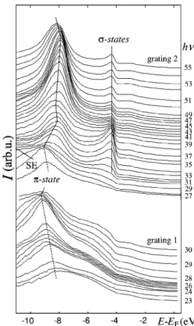
The experimental spectra taken in the energy-distribution-curve 共EDC兲 mode 共smoothed by Gaussian with a 50-meV half-width to reduced the noise兲 are shown in Fig. 1. Our results compare well with previous data obtained on natural single-crystal graphite,1but the spectra are ‘‘cleaner’’ in the
sense of a better spectral contrast due to a better quality of epitaxial graphite. Also the SE intensity is lower due to rela-tively weak higher-order light.
In the low-energy region, the SE structures remain never-theless rather intense, which can impair proper evaluation of the valence-band energies. To suppress their influence, in this region we have measured a series of spectra in the CFS mode by varying h with constant final-state energy
Ef. In these spectra, the SE structures, which are character-ized by Ef⫽const, form only a constant background and thus do not interfere with the peaks from the valence band. These spectra after the noise reduction are shown in Fig. 2. They were normalized to the photon flux using the current from a gold mesh installed after the exit slits of the mono-chromator.
The experimental spectra were insensitive to details of the sample preparation procedure. Only a shoulderlike structure near ⫺5.6 eV, developing at low h, showed some varia-tions and reduced in amplitude upon improvement of the graphite film quality. Lying outside any band dispersion ranges or the regions of high density of states, this structure might not be intrinsic for graphite but due to a remnant sig-nal from the SiC substrate or from Si atoms embedded in the film.
FIG. 1. Experimental normal-emission EDC spectra. Identifica-tion of the spectral peaks is shown. A reverse dispersion of the
-state peak in the low-energy final-state band gap 共see the text
below兲 is indicated by the dashed line.
V. N. STROCOV et al. PHYSICAL REVIEW B 64 075105
III. DISCUSSION A. state
Analysis of the k⬜ dispersions in the valence band re-quires, first of all, knowledge of the PE final bands. The corresponding E(k⬜) is described by complex k⬜, whose imaginary part Im k⬜ accounts for the Bloch wave damping due to finite electron lifetime and coherent scattering off the crystal potential in the band gaps.
Recently, we have performed an independent study of the final bands of graphite using VLEED.7These bands demon-strated dramatic deviations from a free-electron-like disper-sion due to strong perpendicular corrugation of the crystal potential resulting from the quasi-2D layered nature of graphite. The band gaps in the⌫ point were found to extend from 10.8 to 18.6 eV and from⬃36.3 to 42.7 eV. In addition, we estimated the energy dependence of the electron absorp-tion potential Vi, giving the final-state lifetime. These data, as demonstrated on certain transition-metal dichalcogenides,8 allow us to obtain the final-state k⬜ dispersions using a fit-ting procedure. In the present study, focusing on determina-tion of the -state dispersion range along the⌫A line, we will proceed with a simplified model for the final bands.
The final bands were modeled using the empirical pseudo-potential method. The basis included only plane waves with the vectors k⫹G perpendicular to the surface, which is suf-ficient for the main bands coupling to vacuum in the region of interest near the⌫ point.9E(k⬜) was calculated by reduc-ing the secular equation for complex k⬜ to an eigenvalue problem.10The empirical parameters—the effective mass m* and two relevant Fourier components—were determined by setting Vi⫽0 and fitting E(k⬜) to the two experimental band gaps in the ⌫ point. The calculated E(k⬜) is shown in Fig. 3. The dispersions are smoothed due to Vi. The photoelectron escape depth, determined by Im k⬜ as
⫽(Im/k⬜)⫺1, due to wide final-state band gaps dramatically deviates from the usual dependence of a monotonous in-crease upon decreasing h. Note that by using the VLEED data, the obtained E(k⬜) incorporates the true non-free-electron and self-energy effects.
The experimental dispersion of the-state peak in the PE spectra, intriguingly, deviates from that expected from the final-state k⬜dispersion. Indeed, the bottom of theband in the⌫ point 共Fig. 3兲 is reached when the final bands pass this point in the lower-energy band gap at Ef⫽14.5 eV 共taking into account the double-zone dipole selection rules11兲. One would expect that this energy delivers the dispersion mum of the PE peak. However, in the experiment, the mini-mum is ⬃4 eV higher in Ef, closer to the upper edge of the final-state band gap, with a reverse dispersion towards the middle of the gap. This effect does not occur for the upper edge of theband, coupled to the higher-energy pass of the
⌫ point: Ef⫽39.4 eV predicted by the final state E(k
⬜)
agrees well with Ef⫽40⫾0.5 eV corresponding to the maxi-mum of the PE peak dispersion.
The observed peculiarity of the PE response of thestate reveals that the analysis of the k⬜ dispersions requires, be-sides knowing the final-state dispersions, accounting for
in-trinsic effects involved in the PE process that cause shifting
of PE spectral peaks from the true quasiparticle bands, i.e., the dispersions of the peaks of the valence-band spectral function A(,k). These effects are essentially due to the final-state k⬜ broadening Im k⬜ and the initial-state energy broadening Vih⫽h/, whereis the hole lifetime; their com-bination determines the profile of the PE peak, see, e.g., Refs. 12 and 13. Recently, it was noticed that if the initial-state k⬜ dispersion is nonlinear, then the broadenings form an asymmetric PE peak with the maximum shifted from the energy, dictated by the direct transition, toward a larger
inte-FIG. 2. Experimental normal-emission CFS spectra. The spec-tral peaks are identified as in Fig. 1.
FIG. 3. E(k⬜) of the main PE final bands in the region of the band gaps in the⌫ point 共black lines兲 modeled using the VLEED data. Note the smoothing of the k⬜ dispersion due to Viand
dra-matic increase of Im k⬜in the band gaps resulting in decrease of the photoelectron escape depth ⫽(2 Im k⬜)⫺1. For clarity, the inset shows E(k⬜) for Vi⫽0. The lower panel shows the DFT-LDA
cal-culated valence bands from Ref. 7共in the photoemission process, k remains real, contrary to the final bands, because the initial-state wave function is almost undamped due to a very large absorption length of the light兲.
gral number of states within the broadening profile.14,15 Be-low, we will show that this intrinsic effect severely distorts the PE response of thestate.
We modeled the intrinsic effects using the VLEED-derived final bands and assuming the unperturbed bulk band. The PE peak profiles were calculated by analytic integration15 of the expression12,13
I共Ef兲⬀
冕
⫺⬁ ⫹⬁ 1 共k⬜⬘
⫺Re k⬜兲2⫹共Im k⬜兲2 ⫻ 1 关Ef⫺hv⫺Ei共k ⬜⬘
兲兴2⫹共Vi h兲2dk⬜⬘
,where the first term is the final-state Lorentzian k⬜ distribu-tion centered on the final-state Re k⬜, and the second is the initial-state energy distribution centered on the band disper-sion Ei(k⬜). The matrix element and surface transmission factors were assumed to be constant. Ei(k⬜) was approxi-mated by a quadratic dispersion fitted to the DFT calculations.7 The Vih value of ⬃1.9 eV, varying insignifi-cantly within the band, was obtained from the experimental PE peak width using the known final state Im k⬜.
The results of modeling are shown in Fig. 4. In particular, near the band edges, as shown for the bottom of theband, the peaks become asymmetric and shift from the position, dictated by the direct transition, into the band interior 共in-band shifting兲 due to the absence of states beyond the band limits. This effect results in a deviation of the peak disper-sion from the true E(k⬜), which is significant compared to the k⬜dispersion range共similar effects treated in the frame-work of one-step PE calculations are discussed in Ref. 16兲. We stress that this deviation is an intrinsic PE effect that has nothing to do with a deviation of the quasiparticle band from the ground-state picture共see below兲; it reflects how the
qua-siparticle band is measured in the PE experiment, and de-pends on the parameters of the selected final state.
The results give a good qualitative description of the ex-perimental results. The reverse dispersion near the bottom of the band occurs because the increase of Im k⬜ in the cor-responding final-state band gap共Fig. 3兲 is exceptionally large due to a very large gap width and relatively small Vi. This results in an exceptionally large increase of the k⬜ broaden-ing and, therefore, in-band shiftbroaden-ing, which overcomes the trend dictated by the final state E(Re k⬜).17 For the upper edge of the band, coupled to the higher-energy final-state band gap, a similar effect is negligible because, due to the larger Vi and smaller gap width, the relative increase of Im k⬜ is much smaller. Note that if the final bands were described within the usual model of free-electron-like bands, the implied empirical adjustments would mimic the reverse dispersion and this intrinsic photoemission effect would be hidden.
The experimental reverse dispersion range is still⬃0.2 eV larger compared to the model calculation. Though small, this discrepancy may indicate two effects. First, it may have a contribution due to surface effects not included in the model calculation. As in the middle of the final-state band gap the valence-band wave function is probed at reduced com-pared to that near the gap edges共⬃0.8 Å and 1.7 Å corre-spondingly, as determined from Im k⬜in Fig. 3兲. The poten-tial near the surface differs intrinsically from the ideally terminated bulk one due to overlap with the surface barrier and, probably, a minor relaxation of the interlayer distance. This causes a surface modification of the band structure in that the wave function differs from the ideally terminated bulk one, which may result in a shift of the PE peak. The same effect may occur near the upper edge of the band
共⬃1.2 Å兲. Second, the phototransition matrix element may
sharply decrease near the band bottom, a rather common phenomenon for the s p bands, which, in combination with strong broadening of the PE peak, will result in its shift to higher energies.8 The small value of the observed discrep-ancy suggests, however, that neither effect is pronounced.
To achieve the true-band dispersion range, we first de-convoluted the intrinsic effects. The corresponding correc-tions were found near the band extrema from the above model calculations as shown in Fig. 4共for the band bottom, we used the peak dispersion minimum away from the ⌫ point, where increases and the surface effects are reduced兲. With the experimental PE peak dispersing from ⫺9.1 eV
共determined from the CFS spectra兲 to ⫺7.9 eV 共EDC兲, we
obtained the -band dispersion range from ⫺9.3 eV to
⫺7.7 eV with the integral accuracy about ⫾0.1 eV.
Decon-voluting of the matrix element and surface effects is presum-ably also important, but their modeling requires slab band structure and one-step PE calculations, which are computa-tionally difficult and has not been done in this work.
B. Excited-state self-energy effects
The experimental band energies were compared with the theoretical results, calculated in the DFT–local-density-approximation 共LDA兲 framework using the first-principles
FIG. 4. Modeled PE response of the state as the maxima of the PE peaks共dots, which line up in branches according to different final bands兲 on top of the true band dispersion. The deviations, particularly notable in the reverse dispersion near the band bottom, are the intrinsic shifts. The shown peak profile illustrates this effect for the band bottom; the peak maximum at Epis shifted from E0
dictated by the direct transition. The corrections applied to the ex-perimental peak dispersion range are indicated.
V. N. STROCOV et al. PHYSICAL REVIEW B 64 075105
pseudopotential method 共Fig. 5兲. The deviations are signifi-cant, on the whole ⬃1 eV. In our case, the error introduced by the LDA is presumably insignificant 共for the valence band, the LDA and generalized gradient approximation give almost identical results7兲. The deviations occur, therefore, because the dynamic electron exchange-correlation potential, expressed by the self-energy⌺, differs from the static DFT one Vxc. The self-energy corrections to the band energies are determined by the expectation values ⌬⌺⫽
具
兩Re⌺⫺Vxc兩
典
. The observed⌬⌺ show a band dependence: thestates, despite being closer to EF, are more strongly shifted compared to thestate.
The results of a first-principles quasiparticle calculation are also shown in Fig. 5. The self-energy operator was evalu-ated here within the GW approximation based on the DFT-LDA pseudopotential scheme.18,19 The calculation repro-duces well the direction and average magnitude of the ⌬⌺ shifts to within a few tenths of an eV.
The band dependence of⌬⌺ may be related to the spatial localization of the one-electron wave functions determined by their overlap with the varying valence electron density
n(r) 共the core electrons make a negligible contribution to the
dynamic self-energy effects in the valence band due to large energy separations and thus weak virtual scattering from them兲.15,20This effect can be expressed through an effective wave-function-weighted density
具
n典
⫽兰n(r)兩(r)兩2dr. Thecalculation in Fig. 6 shows that the states are weighted mainly in the interlayer region. They experience thus a small effective
具
n典
⫽0.105 (a.u.)⫺3. The states are weighted, on the contrary, within the layers with large electron density and experience a large具
n典
⫽0.208(a.u.)⫺3. Concomitantly, the states have a much stronger expectation value具兩Re ⌺兩典 of the self-energy, in our GW calculation⫺17.3 eV, than the state value 具兩Re ⌺兩典⫽⫺13.1 eV. This effect, however, is already found within the DFT-LDA, which yields almost thesame difference between
具
兩Vxc兩典
and具
兩Vxc兩典
. The GWcalculated ⌬⌺ are therefore basically equal for both states. Nevertheless, for many systems such as Cu the dynamic exchange-correlation has a stronger dependence on the elec-tron density than the static one, and a selec-tronger localization of a state in a high-density region with a larger value of
具
n典
leads to a stronger ⌬⌺.15,20The observed band dependence of ⌬⌺ in Fig. 5 seems to indicate that this behavior is also present in graphite. It is an open question as to why this effect is not found in the present GW results. It should be noted that an analysis of the specific physical origins of the
⌬⌺ shifts is highly sensitive to the numerical accuracy of the GW and DFT calculations, as the difference between the
dynamic and static exchange-correlation is normally less than 10% of the total value.
IV. CONCLUSION
Refined PE measurements on graphite have been per-formed using an epitaxially grown high-quality sample. The valence band along the layer-perpendicular⌫A line of theBZ was studied in detail. Interpreted using VLEED experimental data on the final bands, the PE data have revealed new pe-culiarities of the electronic structure of this prototype layered material.共i兲 PE response of the band is severely distorted by intrinsic broadening effects, which narrow the observed band dispersion and can even reverse it. Similar effects can occur in other layered materials whose final bands are highly structured due to their quasi-2D nature. The experimental data deconvoluted from the intrinsic effects place the band along the ⌫A line from ⫺9.3 to ⫺7.7 eV, but these figures are still to be improved against the surface and matrix ele-ment effects.共ii兲 The experimental valence band experiences significant excited-state self-energy effects whose band de-pendence is connected with the spatial localization of the one-electron wave functions.
*Present address: Experimentalphysik II, Universita¨t Augsburg, D-86135 Augsburg, Germany, and the Institute for High-Performance Computations and Databases, P.O. Box 71, 194291 St. Petersburg, Russia.
1A.R. Law, M.T. Johnson, and H.P. Hughes, Phys. Rev. B 34, 4289
共1986兲.
2C. Heske, R. Treusch, F.J. Himpsel, S. Kakar, L.J. Terminello,
H.J. Weyer, and E.L. Shirley, Phys. Rev. B 59, 4680共1999兲.
FIG. 5. Comparison of the experimental- and -state energies with the DFT-LDA and quasiparticle GW calculations.
FIG. 6. Total valence charge density n(r) and individual charge density兩(r)兩2of the state and of the state 共averaged along the graphene layers兲 depending on the layer-perpendicular z coordinate perpendicular to the layers. The vertical arrows indicate the position of the graphene layers.
3A.J. Van Bommel, J.E. Crombeen, and A. Van Tooren, Surf. Sci.
48, 463共1975兲.
4L. Muehlhoff, W.J. Choyke, M.J. Bozack, and J.T. Yates, J. Appl.
Phys. 60, 2842共1986兲.
5A. Charrier, A. Coati, F. Thibaudau, J.-M. Debever, M.
Sauvage-Simkin, Y. Garreau, R. Pinchaux, and J.-M. Themlin 共unpub-lished兲.
6I. Forbeaux, J.-M. Themlin, and J.-M. Debever, Phys. Rev. B 58,
16 396共1998兲.
7V.N. Strocov, J.-M. Themlin, J.-M. Debever, H.I. Starnberg, P.
Blaha, M. Rohlfing, and R. Claessen, Phys. Rev. B 61, 4994
共2000兲.
8V.N. Strocov, H. Starnberg, P.O. Nilsson, H.E. Brauer, and L.J.
Holleboom, Phys. Rev. Lett. 79, 467共1997兲; J. Phys.: Condens. Matter 10, 5749共1998兲.
9Our modeling misses therefore the band gaps due to hybridizatin
with other plane waves. Most notable of such band gaps is placed near 30 eV 共see Ref. 7兲. In the PE spectra, the corre-sponding distortion of the final-state dispersion is reflected by distorted dispersion of the state peak in the h range from 32 to 38 eV, see Fig. 1.
10J.B. Pendry, J. Phys. C 2, 2273共1969兲.
11D. Pescia, A.R. Law, M.T. Johnson, and H.P. Hughes, Solid State
Commun. 56, 809共1985兲.
12Angle-Resolved Photoemission, edited by S.D. Kevan共Elsevier,
Amsterdam, 1992兲.
13R. Matzdorf, Appl. Phys. A: Mater. Sci. Process. 63, 549共1996兲. 14V.N. Strocov, in Electron Spectroscopies Applied to
Low-dimensional Materials共Kluwer, The Netherlands, 2000兲.
15V. N. Strocov et al., Phys. Rev. B 63, 205108共2001兲.
16E. Pehlke and W. Schattke, Solid State Commun. 69, 419共1989兲;
T. Strasser, F. Starrost, C. Solterbeck, and W. Schattke, Phys. Rev. B 56, 13 326共1997兲.
17The reverse dispersion may in principle limit the accuracy of the
three-dimensional band mapping using the band-gap emission
关V.N. Strocov et al., Phys. Rev. Lett. 81, 4943 共1998兲 and Ref.
15兴, but it appears only in exceptionally wide final-state band gaps.
18M.S. Hybertsen and S.G. Louie, Phys. Rev. Lett. 55, 1418共1985兲;
Phys. Rev. B 34, 5390共1986兲.
19M. Rohlfing, P. Kru¨ger, and J. Pollmann, Phys. Rev. B 52, 1905
共1995兲.
20P.O. Nilsson and C.G. Larsson, Phys. Rev. B 27, 6143共1983兲.
V. N. STROCOV et al. PHYSICAL REVIEW B 64 075105