HAL Id: tel-03137675
https://tel.archives-ouvertes.fr/tel-03137675
Submitted on 10 Feb 2021HAL is a multi-disciplinary open access
archive for the deposit and dissemination of sci-entific research documents, whether they are pub-lished or not. The documents may come from teaching and research institutions in France or abroad, or from public or private research centers.
L’archive ouverte pluridisciplinaire HAL, est destinée au dépôt et à la diffusion de documents scientifiques de niveau recherche, publiés ou non, émanant des établissements d’enseignement et de recherche français ou étrangers, des laboratoires publics ou privés.
Epitaxie de couches d’alliages quaternaires à base
d’InAIGaN pour les transistors de haute performance
Mrad Mrad
To cite this version:
Mrad Mrad. Epitaxie de couches d’alliages quaternaires à base d’InAIGaN pour les transistors de haute performance. Science des matériaux [cond-mat.mtrl-sci]. Université Grenoble Alpes [2020-..], 2020. Français. �NNT : 2020GRALY023�. �tel-03137675�
THÈSE
Pour obtenir le grade de
DOCTEUR DE L’UNIVERSITE GRENOBLE ALPES
Spécialité : Physique des matériauxArrêté ministériel : 25 mai 2016
Présentée par
Mrad MRAD
Thèse dirigée par Guy FEUILLET et encadrée par Matthew CHARLES Préparée au sein du CEA-LETI
Dans l'École Doctorale de Physique - Grenoble
Epitaxie de couches d’alliages
quaternaires à base d’InAlGaN
pour les transistors de haute
performance
Thèse soutenue publiquement le 7 Juillet 2020 devant le jury composé de:
Mme Sylvie CONTRERAS
Chargée de recherche, Université de Montpellier II, Rapporteur
M. Yvon CORDIER
Directeur de Recherche, CRHEA - CNRS Valbonne, Rapporteur
M. Etienne GHEERAERT
Professeur, Université Joseph Fourier - Institut Néel, Président
Mme Marie LESECQ
Maître de conférences, Université de Lille 1, Examinateur
Mme Rachel OLIVER
Professeur, Université de Cambridge, Examinateur
M. Guy FEUILLET
Directeur de Recherche, CEA-LETI, Directeur de thèse
M. Matthew CHARLES
Acknowledgments
This PhD work has been carried out at the CEA-LETI laboratory in Grenoble. Behind this achievement, there are a great many people, who gave me help, support and inspiration so that it was made possible. Therefore, I take this opportunity to express my special gratitude to all of them for contributing to my thesis success.
First, I would like to genuinely thank my thesis director Guy Feuillet for believing in me and giving me the opportunity to join the LETI lab and conduct three years of research under his direction. Guy is someone you will instantly love and never forget once you meet him. He’s the funniest advisor and one of the smartest people I know. I would like to thank him for having given me his vision of research and his working methods in order to guarantee the rigor required by the scientific work.
I thank the members of my thesis jury, Dr. Sylvie Contreras, Dr. Yvon Cordier, Prof. Etienne Gheeraert, Dr.
Marie Lesecq, and Prof. Rachel Oliver for devoting their time to read this manuscript. Furthermore, I would like to
thank them for their constructive comments and remarks.
My warmest thanks go to my thesis supervisor Matthew Charles to whom I present my deep gratitude for his excellent supervision, his many advices and for all the hours he devoted to the good conduct of this research work. I am sure that I could not have done all the work without his encouragements, motivation and patience. I would also like to tell him how much I appreciated his great availability and his respect for the tight deadlines for proofreading the documents I sent to him. Finally, I was very sensitive to his good humor which made our collaboration very pleasant.
In addition, I would like to cordially thank the following lab members who have been of assistance to me during my PhD in a wide variety of roles: Laurent Vandroux, Sylvain Maitrejean, Anne Roule, Lucile Roulet,
Amelie Dussaigne, Pierre Ferret, Yann Mazel, Jérôme Richy and Matthieu Lafossas.
I would also like to extend my gratitude to my closest friends who never wavered in their support: Rami
Khazaka, Christelle Salameh, Salim Assaf, Rodaina Aboul Hosn, Halim Hanna, Roy Dagher, Tamara Oueidat, Houssein Dirani, Jessy Hasna, Elias Haber, Elio Asmar, Hassan Dirani, Georgio Zemar, Carole Pernel, Victor Yon, Rebecca Chahine, Samer Dagher, Loraine Youssef, Benjamin Samuel, and Sofia Boughaleb. I will never
forget the good times we shared together.
My special thanks go then to my girlfriend Joyce Stephan, definitely you were a source of inspiration and determination. You came at the perfect time. Thank you for motivating and filling me with affection during moments of doubt and weakness. Thank you for never giving up on me. My love, this thesis is ours, and its end heralds a new step for both of us. I can't wait to find out what awaits us!
Last but not least, and with great affection, I would like to thank every member of my family for their unconditional and unlimited support. Particularly, I would like to thank my beloved parents, Bayeh Georges Mrad and Emmeh Samira Mrad, to whom this PhD is dedicated. Bayeh, Emmeh, I can never express to you how proud I am to have you as parents. Thank you for being my first fans, and for giving me exceptional attention and confidence since the first second of my life. I will never forget the nights you spent watching over my morals, my health and my studies. Thank you for your sacrifice, love, comfort and unconditional support. Without you, I could never have done all this! I would also like to thank my beloved sisters Marguerite Mrad and Christine Mrad and my brother Elie
Mrad. It is a blessing to have someone to count on. All these years, you have always been my rock and my shield.
You kept me away from harm and guided me with your advices. I would not be who I am now if not for you. Thank you! Your endless love, support and invaluable help made it all possible and brought this work to a happy end.
Mrad Mrad
GENERAL TABLE OF CONTENTS
Chapter I: Nitride semiconductors ... 0
I.1 Introduction ... 1
I.2 III-Nitride and historical key events ... 2
I.3 III-Nitride properties ... 3
I.3.1 Substrate of choice ... 3
I.3.2 Crystalline structures ... 5
I.3.3 Spontaneous polarization ... 7
I.3.4 Piezoelectric polarization ... 9
I.3.5 Polarization induced charge and two-dimensional electron gas ... 13
I.3.6 Specificities of the III-N elements for electronic applications ... 15
I.4 GaN on Si based electronic applications ... 18
I.4.1 InAlN/GaN HEMT ... 20
I.4.2 State of the art: InAlN/GaN HEMTs Rsheet, ns, µ ... 21
I.5 Objective of this research... 22
Chapter II: III-N MOVPE growth and characterization methods ... 26
II.1 Introduction ... 27
II.2 The different epitaxial growth techniques of GaN ... 28
II.3 MOVPE growth technique ... 29
II.3.1 MOVPE basics ... 29
II.3.2 MOVPE growth analysis ... 31
II.3.3 Important quantities and concepts of MOVPE ... 34
II.3.3.1 Diffusion across boundary layer and maximum growth rate ... 34
II.3.3.2 The source molecules for III-N MOVPE growth ... 36
II.3.3.3 Parasitic gas phase reactions ... 37
II.3.3.4 V/III ratio and partial pressures... 38
II.4 MOVPE growth equipment: AIXTRON CCS ... 39
II.4.1 Overall tool setup... 40
II.4.2 Bubbler operation ... 43
II.4.3 In-situ characterizations ... 44
II.4.3.1 Wafer curvature measurements ... 44
II.4.3.2 Emissivity-corrected pyrometry ... 48
II.4.3.3 Two-wavelength reflectance ... 50
II.5 Standard HEMT buffer epitaxial heterostructure ... 52
II.6 Characterization techniques ... 54
II.6.1 Morphological characterization ... 55
II.6.1.1 Atomic Force Microscopy... 55
II.6.2 Optical characterization ... 58
II.6.2.1 Low-Temperature Photo-Luminescence spectroscopy ... 58
II.6.2.2 Wavelength Dispersive X-Ray Fluorescence... 60
II.6.3 Structural characterization ... 61
II.6.3.1 X-Ray Reflectivity ... 61
II.6.3.2 High-Resolution X-Ray Diffraction ... 64
II.6.4.1 Secondary Ion Mass Spectrometry ... 68
II.6.4.2 Plasma Profiling Time of Flight Mass Spectrometry ... 69
II.6.5 Electrical characterization ... 71
II.6.5.1 Four-Point Probe ... 71
II.7 Summary ... 73
Chapter III: Understanding Ga contamination in InAlN barrier layers 76
III.1 Introduction ... 77III.2 Experimental details ... 78
III.3 Results and discussion ... 80
III.4 Hydrogen and chlorine etching ... 90
III.5 Post-etch pure InAlN barrier layers growth ... 94
III.6 Conclusion ... 100
Chapter IV: Understanding Ga contamination in InGaN layers ... 102
IV.1 Introduction ... 103
IV.2 Experimental details ... 103
IV.3 Results and discussion ... 105
IV.4 Conclusion ... 115
Chapter V: Overcoming Ga contamination in Close Coupled Showerhead
reactors ... 120
V.1 Introduction ... 121
V.2 Tests to avoid Ga pollution ... 123
V.2.1 AlGaN buffers regrowth ... 123
V.2.2 Nitridation of the shield ... 126
V.2.3 16.5 mm Sample-Shield growth gap ... 131
V.2.4 Low temperature 200 nm GaN regrowth under H2 ... 135
V.2.5 Increasing shield temperature during GaN regrowth ... 138
V.3 Conclusion ... 145
LIST OF FIGURES
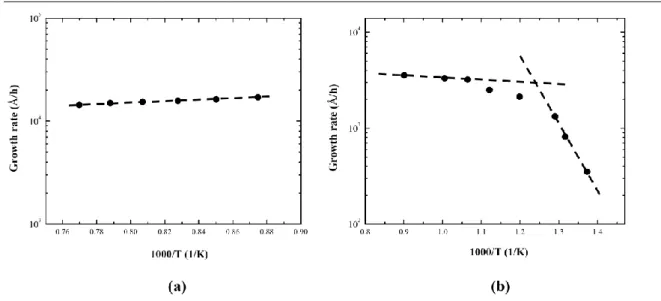
Figure 1: Illustration of a) rock-salt b) zinc-blende and c) wurtzite crystal structures. ... 6 Figure 2: a) III-N wurtzite crystal structure showing the two interpenetrating hexagonal lattices. b) crystallographic orientation [0001] and c) [0001] as a function of gallium and nitrogen polarity. ... 7 Figure 3: a) Tetrahedron bonding showing dipolar moments and spontaneous polarizations. b) Macroscopic spontaneous polarization and charge repartition at the interfaces of c-axis metal-face of III-N structure. ... 8 Figure 4: a) Spontaneous polarization as a function of Al ratio in wurtzite III-N ternary alloys. b) Evolution of the band gap energy of III-N alloys depending on the lattice parameter... 9 Figure 5: Illustration of a) tensile and b) compressive strains. c) InAlN/GaN strained heterostructure and d) compressed heterostructure. ... 10 Figure 6: a) III-N HEMT heterostructure,with the equilibrium band diagram (V = 0 Volts) of the InAlN/GaN heterostructure above b) total polarization induced sheet charge σ/e (Psp+Ppe) bound at the interfaces of Ga-face AlGaN/GaN, AlInN/GaN and InGaN/GaN heterostructures, versus alloy composition of the top layer [38]. ... 14 Figure 7: Bandgap energy of different semiconductors depending on the lattice parameter at 300 K. ... 16 Figure 8: Si, SiC, GaAs, GaN capability comparison for electronic applications. [data from Table 3 and Table 1] ... 19 Figure 9: Frequency-accessible power ranges for different semiconductor materials reproduced from [53]. ... 20 Figure 10: InAlN/GaN sheet resistance values for different substrates in function of years of development, and black dashed line present typical AlGaN/ GaN Rsheet values. [64, 65, 66, 67, 68, 69, 70, 71, 72, 73] [74, 75, 76, 77, 78, 79, 80, 81, 82, 83] [84, 85, 86, 87, 88, 62, 89, 90, 91, 92] [93, 94, 95, 63, 96, 60, 97, 98, 99, 100] [101, 102, 103, 104, 105, 106, 61, 107, 108, 109] [110, 111, 112]... 22 Figure 11: Total polarization in InAlGaN barriers for increased Ga% and fixed In/(In+Al) ratio of 18%... 23 Figure 12: Simple illustration of the epitaxy process. ... 30 Figure 13: MOVPE chemical processes in parallel with physical processes. ... 31 Figure 14: Growth efficiency of GaAs as a function of the reciprocal growth temperature. [120] [121] [122] [123] ... 32 Figure 15: (a) PhD experiments on GaN growth rate under NH3 for temperatures ranging
from 870 °C to 1040 °C. (b) Work of S. Fujieda et Al. [125] on GaN growth rate under NH3
for temperatures ranging from 450 °C to 850 °C... 34 Figure 16: Illustration of the boundary layer 𝛿0 close the growing surface. ... 35
Figure 17: Illustration of III-N MOVPE precursor molecules: (a) trimethyl(Ga, Al, In) (b)
triethyl(Ga, Al, In) ... 36
Figure 18: The different geometries of III-N growth equipments. ... 39
Figure 19: On the left, photo of the AIXTRON CRIUS R200 tool. Bottom right a view of the SiC coated graphite susceptor with the 200 mm diameter Si wafer. Top right a view of the showerhead with the shield. ... 40
Figure 20: Simplified gas lines in AIXTRON CRIUS R200 tool. ... 41
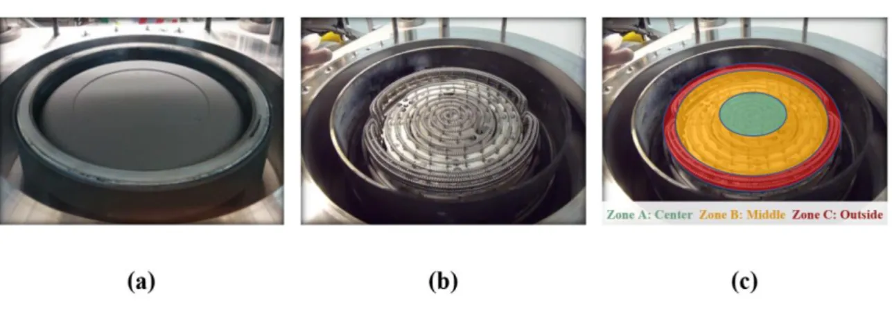
Figure 21: a) SiC coated graphite susceptor, b) the heater coils, and c) the three zones of heating. ... 42
Figure 22: Wafer bow detection with two LASER beams and the associated 2D CCD camera observations. ... 45
Figure 23: Geometric parameters that define wafer bow. ... 45
Figure 24: Basics of GaN on silicon growth. ... 47
Figure 25: The reasons for wafer bow: a) temperature gradient, b) lattice mismatch, and c) CTE difference. ... 47
Figure 26: Black-body spectrum for temperatures between 300 K and 1000 K in a linear diagram. ... 48
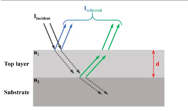
Figure 27: Schematic of the optical configuration of a light beam reflectance measurement. ... 50
Figure 28: Fabry-Pérot oscillations cases, in a) an ideal growth case where the top layer is transparent and it has a very smooth surface, b) an absorbent material case, and in c) a case of a roughening surface. ... 51
Figure 29: Schematic of HEMT growth structures. ... 52
Figure 30: The main techniques used for HEMT structure characterization. ... 54
Figure 31: AFM equipment with FastScan system mounted. ... 55
Figure 32: Schematic diagram of a typical AFM setup. ... 56
Figure 33: Variation of force with tip-surface distance. ... 56
Figure 34: Luminescence mechanisms from a direct band gap semiconductor material. ... 59
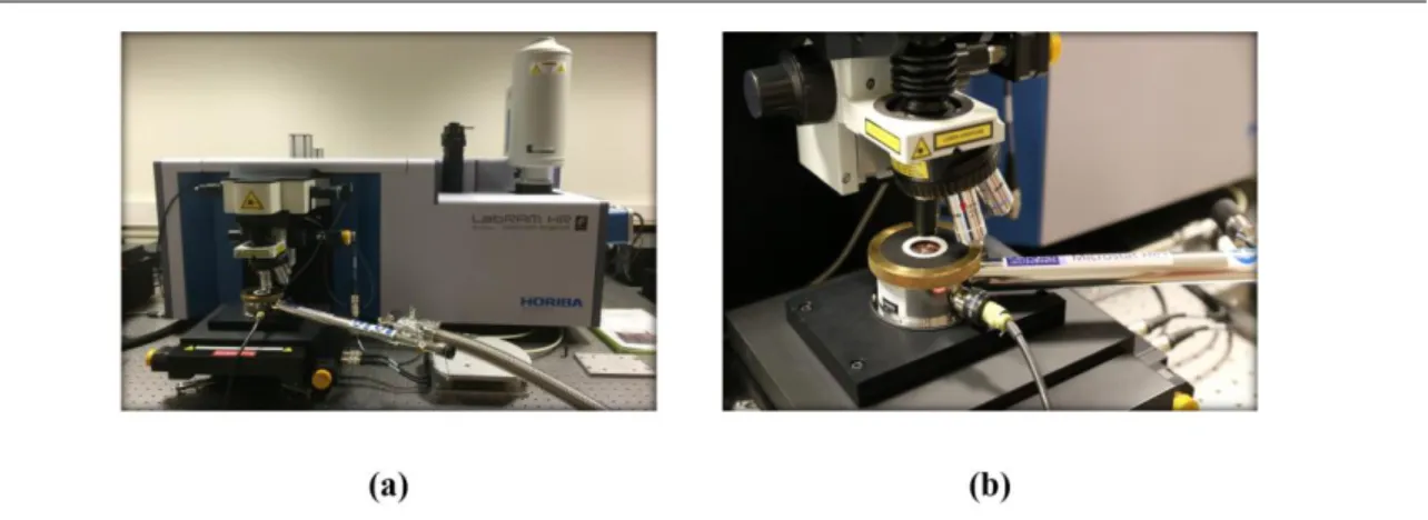
Figure 35: a) Horiba LabRAM HR tool, b) the objective microscope turret with the removable He cryostat. ... 59
Figure 36: Visualization of the principle of X-Ray Fluorescence. ... 60
Figure 37: Spectrometer tool: RIGAKU AZX400... 61
Figure 38: XRR measurement principle. ... 62
Figure 39: XRD/XRR tool: XRD3 JV/BRUKER, DELTA-XM. ... 64
Figure 40: Diagram of the principle of Bragg's law. ... 65 Figure 41: A section through reciprocal space for a c-oriented GaN film. The regions shown in grey are the inaccessible regions (where the sample blocks one of the beams). k0, kh, and
S are respectively the incident, diffracted and scattering vectors with respect to the crystal.
Figure reproduced from [140]. ... 65
Figure 42: XRD schematic configuration with the most commonly used angles... 66
Figure 43: Schematic diagram of the SIMS principle. ... 68
Figure 44: Schematics of glow discharge plasma for depth profiling analysis. ... 69
Figure 45: PP-TOFMS tool: Jobin1 Horiba Scientific. ... 70
Figure 46: SIAM tool. ... 71
Figure 47: Rsheet measurement setup. ... 72
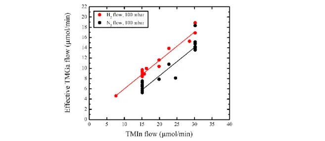
Figure 48: Relationship between effective TMGa generated, and TMIn intentionally flowed into the growth chamber under N2 and H2. Data from [150] ... 78
Figure 49: Production rates of InN, AlN, GaN as a function of (a) TMIn and (b) TMAl flow rates. Reproduced from [152] ... 78
Figure 50: Schematic of growth structures. ... 79
Figure 51: SIMS and calibrated PP-TOFMS measurements for all 5 samples with and without GaN regrowth. ... 81
Figure 52: InAl(Ga)N barriers composition of as a function of regrown GaN thickness. ... 81
Figure 53: Indium WDXRF peak (left) and aluminum WDXRF peak (right) for all 5 samples. ... 82
Figure 54: Barrier thickness measured by XRR (black line), Al composition in barrier (blue line/ ) and the product (blue line/X): versus GaN regrowth thickness. ... 82
Figure 55: III-N incorporated mass in InAlN layers as a function of GaN regrowth thickness. ... 83
Figure 56: 2µm x 2µm AFM scans of the 5 samples. ... 84
Figure 57: Schematic of proposed gallium contamination mechanism. ... 85
Figure 58: Incorporation rates for Al, Ga and In and Xreact. Xreact is calculated for a fixed In incorporation rate of 10%. ... 88
Figure 59: Sheet resistance versus GaN regrowth thickness for HEMT with InAlGaN barrier. ... 88
Figure 60: Spontaneous and piezoelectric polarizations of the 5 samples of InAlGaN barrier layers. ... 90
Figure 61: 5µm x 5µm and 2µm x 2µm AFM scans showing a typical GaN surface morphology without etch. ... 91
Figure 62: 2µm x 2µm AFM scans showing GaN surface morphology after performing (a) 40 nm H2 etch, (b) 10 nm Cl2 etch and (c) 1 nm Cl2 etch. ... 91
Figure 63: 2µm x 2µm AFM scans with PP-TOFMS measurements of InAlN/AlN/GaN heterostructures showing HEMT surface morphology and barrier composition after performing (a) 40 nm H2 etch, (b) 5 nm H2 etch and (c) 1 nm Cl2 etch. ... 92
Figure 64: Sheet resistance for InAlN/AlN/GaN HEMT structures for chlorine and hydrogen
etched samples compared with GaN regrowth samples. ... 93
Figure 65: Schematic of growth structures of InAlN barrier layers with different In%. Growth is carried out on the GaN template after a growth intrerruption followed by Cl2 chamber cleaning and 5 nm H2 etch. ... 94
Figure 66: InAlN Barrier thickness measured by XRR for different nominal In compositions ... 95
Figure 67: calibrated PP-TOFMS measurements for all 5 InAlN samples. ... 96
Figure 68: 2µm x 2µm AFM scans of all InAlN barrier layers with different In%. ... 97
Figure 69: Rsheet measurements of the 5 InAlN samples grown onto 5nm H2 etched GaN templates with different In% (in black) and in green the first 5 nm H2 etched sample that we have shown in Figure 63 (b). ... 97
Figure 70: 2µm x 2µm AFM scans with PP-TOFMS measurements of InAlN/AlN/GaN heterostructures with different TMIn growth flows... 98
Figure 71: Rsheet measurements in function of In% for all etched samples. Blue, black and green points correspond to the samples shown in Figure 70, Figure 68, and Figure 63 (b) respectively. ... 99
Figure 72: Schematic of growth structures. ... 104
Figure 73: RSM (114) measurements of set A (TMGa as Ga source) and set B (TEGa as Ga source)samples. ... 106
Figure 74: XRD ω-2θ measurements of set A (green) and B (red). ... 106
Figure 75: 2µm x 2µm AFM scans of set A (TMGa as Ga source) and B ( TEGa as Ga source). ... 107
Figure 76: LT-PL spectra: InGaN normalized intensity as a function of photon energy at 6K (solid lines) and the fitted data (dash lines). ... 108
Figure 77: a) InGaN layers thickness of set A and B deduced from XRD. B) In% in InGaN layers of set A and B deduced from XRD and LT-PL. ... 108
Figure 78: (0002) XRD ω-2θ measurements of set C. ... 110
Figure 79: RSM (114) measurements of set C samples. ... 110
Figure 80: 2µm x 2µm AFM scans of set C. ... 110
Figure 81: (a) LT-PL spectra: InGaN normalized intensity as function of photon energy at 6K(solid lines) and the fitted data (dash lines). (b) InGaN layer thickness and In% in InGaN layers as deduced from XRD and LT-PL. ... 111
Figure 82: III-N incorporated mass into InAlN and InGaN as a function of GaN regrowth thickness. ... 112
Figure 83: XRD ω-2θ measurements of set D and one sample of set C (TMIn: 400 sccm) of samples grown (a) in cleaned reactor and (b) with 200 nm GaN regrowth. ... 113
Figure 84: 2µm x 2µm AFM scans of samples grown in cleaned reactor of set D and one sample of set C (TMIn: 400 sccm). ... 113
Figure 85: (a) In% in InGaN layers and (b) InGaN layers thickness as a function of TMIn flow. ... 114 Figure 86: The potential origins of Ga pollution on the shield. ... 121 Figure 87: Percentage pyrolysis versus temperature for TMGa in ambients of H2 and N2.
[120] ... 122 Figure 88: Schematic of growth structures of InAlN barriers on the top of AlGaN buffers with different Al%. ... 123 Figure 89: 2µm x 2µm AFM scans of InAlN barriers grown on the top of AlGaN and GaN buffers. ... 124 Figure 90: XRR measurements of the InAlN barriers for AlGaN and GaN buffers. ... 124 Figure 91: PP-TOFMS measurements for samples grown with 25 nm of AlGaN with different Al% and GaN. ... 125 Figure 92: Sheet resistance for samples grown with 25 nm of AlGaN with different Al% and GaN buffers. ... 126 Figure 93: Diagram showing growth chamber during the nitridation step for sample (a), (b) and (c). ... 128 Figure 94: Schematic of growth structures during nitridation experiment for sample (a), (b) and (c). ... 128 Figure 95: XRR measurements for the 200 nm GaN regrowth sample and the nitridation samples. ... 129 Figure 96: 2µm x 2µm AFM scans with PP-TOFMS measurements of the nitridation samples (a), (b), and (c) and the 200 nm GaN regrowth sample. ... 129 Figure 97: Rsheet measurements of the nitridation samples (a), (b), and (c) and the 200 nm GaN regrowth sample compared to the state of the art Rsheet value of InAlN on GaN on Si HEMTs [62]. ... 130 Figure 98: Schematic growth structure of the sample with 16,5 nm sample-shield gap. .. 132 Figure 99: XRR measurements for the set of GaN regrowth samples of chapter 3 in black, including the 50 nm GaN regrowth sample (11 mm sample-shield gap) and the 70 nm GaN regrowth sample in red (16.5 mm sample-shield gap). ... 133 Figure 100: 2µm x 2µm AFM scans with PP-TOFMS measurements of the 70 nm GaN regrowth sample (16.5 mm sample-shield gap) and the 50 nm GaN regrowth sample of chapter 3 (11 mm sample-shield gap) ... 133 Figure 101: PP-TOFMS measurements of the set of GaN regrowth samples of chapter 3 open squares, including the 50 nm GaN regrowth sample (11 mm sample-shield gap) and the 70 nm GaN regrowth sample full squares (16.5 mm sample-shield gap). ... 134 Figure 102: Rsheet measurements of the set of GaN regrowth samples of chapter 3 in black, including the 50 nm GaN regrowth sample (11 mm sample-shield gap) and the 70 nm GaN regrowth sample in red (16.5 mm sample-shield gap). ... 135 Figure 103: Schematic growth structures of the 960 °C and the 880 °C GaN regrowth samples. ... 136
Figure 104: XRR measurements for the 1040 °C, 960 °C and 880 °C GaN regrowth samples. ... 136 Figure 105: 2µm x 2µm AFM scans with PP-TOFMS measurements of the 1040 °C, 960 °C and 880 °C GaN regrowth samples. ... 137 Figure 106: (a) Rsheet measurements and (b) calculated barriers polarizations of the 1040 °C, 960 °C and 880 °C GaN regrowth samples. ... 138 Figure 107: The two growth chamber configurations used for the increase of shield T during GaN growth. ... 139 Figure 108: Schematic of grown structures, a) configuration (A) (samples A1 to A7), b) configuration (B) (sample B). ... 140 Figure 109: Ga% in InAlN layers as a function of the shield temperature during GaN growth. [180] ... 142 Figure 110: 2µm x 2µm AFM scans with PP-TOFMS measurements for the 200 nm GaN regrowth samples under N2 with different growth rates. ... 144
Figure 111: Rsheet measurements for the 200 nm GaN regrowth samples under N2 with
LIST OF TABLES
Table 1: Most used bulk substrates for wurtzite GaN growth. [21]... 4 Table 2: Different properties of III-Nitride binaries wurtzite crystal: bandgap energy and lattice parameter at 300K, spontaneous, piezoelectric, and elastic parameters. [1, 2, 3, 25, 26, 27, 28, 29, 30, 31] [32]... 12 Table 3: Properties of different semiconductor materials at 300K. [40, 41, 42, 43] ... 16 Table 4: Comparison of normalized figures of merit of various semiconductors. [50] [46] [47] [48] [49]... 18 Table 5: Comparative of epitaxial growth techniques of III-N semiconductors. [119] [120] ... 28 Table 6: TM precursors dissociation reactions & their free Gibbs energy change for the dissociation. [127] ... 37 Table 7: Chemical properties of group III organometallic precursors, and constants for calculating the vapor pressure in Torr. [120] ... 44 Table 8: InAl(Ga)N barriers composition and lattice parameter of as a function of overgrown GaN thickness. ... 84 Table 9: Calculated spontaneous and piezoelectric polarizations in the InAlGaN barrier layers. ... 89 Table 10: Hydrogen and chlorine etching conditions. ... 91 Table 11: TMIn and TMAl flow values used for the growth of InAlN barriers with different In%.. ... 95 Table 12: InGaN and InAlN MOVPE growth conditions for samples grown in clean and gallium polluted chamber. ... 105 Table 13: Nitridation step anneal conditions. ... 127 Table 14: Description of the samples grown in this study. ... 140
General introduction
The optical, electrical, mechanical, and thermal properties of the group III-N semiconductors make them excellent materials for many electronic and optoelectronic applications. In particular, the high breakdown field, high electron mobility and high thermal conductivity favor their use for high power transistors and diodes, and for radio-frequency transistors. The work of this thesis is mainly focused on the metal organic vapor phase epitaxy (MOVPE) growth of III-N materials, in particular InAlN/GaN structures on 200 mm silicon substrates for high power performance high electron mobility transistors (HEMTs).
Currently, CEA-LETI produces GaN based HEMTs on Si(111) wafers using AlGaN/GaN heterostructures. However, the growth of InAlN barriers on GaN buffers has demonstrated the possibility to surpass AlGaN on GaN performance. On the other hand, growing high quality InAlN/GaN HEMTs is in general more difficult than growing its AlGaN/GaN counterparts. This issue comes from the strong immiscibility effect between InN and AlN, resulting from their big lattice parameter difference. Another challenge is the big difference in growth parameters of its two binaries InN and AlN which makes it difficult to optimize the growth conditions. Finally, a serious problem in Close Coupled Showerhead (CCS) MOVPE growth chambers for the growth of pure InAlN barriers is the non-intentional incorporation of Ga. Gallium pollution affects the control and the reproducibility of the desired growth recipes of InAlN barriers. This therefore also affects the structural and electrical properties of these ternary epilayers. The objectives of this work are to firstly understand and control the gallium contamination in CCS reactors, and later to find a solution to avoid this contamination through the understanding of the main parameters affecting it. Achieving these two main objectives would enable us to grow well controlled and pure InAlN barriers.
In the first chapter of this work, after highlighting the key historical events of the III-Ns developments, we will detail their general properties. We will deal with the different substrates that allow GaN crystalline growth and detail the different crystalline structures that can be grown. Then we will investigate III-N intrinsic material properties with a focus
on the polarization effects. Later, we will discuss the use of the III-N elements for electronic applications, mainly in the fields of power and high frequency electronics, with a focus on InAlN/GaN/Si HEMT where we present the state of the art of Rsheet values.
The second chapter combines experimental and theoretical details. In a first part we will examine the different epitaxial techniques used for the growth of III-N semiconductor materials, with a focus on MOVPE, the method we used for the growth of our III-N samples. Next, we will detail the AIXTRON growth equipment and its different parts, which are critical for the good control of the MOVPE growth epitaxy of III-N layers. In a second part, we will discuss the different physical and chemical characterizations techniques we frequently performed during this work: Atomic Force Microscopy (AFM) for morphological characterization, Low-Temperature Photo-Luminescence spectroscopy (LT-PL) and Wavelength Dispersive X-Ray Fluorescence (WDXRF) for optical characterization, High Resolution X-Ray Diffraction (HR-XRD) and X-Ray Reflectivity (XRR) for structural characterization, Secondary Ion Mass Spectrometry (SIMS) and Plasma Profiling Time of Flight Mass Spectrometry (PP-TOFMS) for chemical characterization and finally Four-Point Probe (4PP) for electrical characterization.
In the third chapter, we will be focusing on understanding and quantifying the gallium contamination problem in the AIXTRON CCS chamber architecture on the MOVPE growth of InAlN barrier layers. We show reduced indium incorporation and increased gallium non-intentional incorporation in the InAlN barrier layers along with an increase in the thickness of these layers as the gallium contamination increases. Here, we propose a quantitative model for these observations where we suggest that the TMIn precursor reacts with gallium on the showerhead shield surface to release TMGa, which is then incorporated as Ga into the layers. We showed the possibility of avoiding gallium pollution by growing the barrier layers directly on a GaN template after removing the samples from the chamber and cleaning the chamber. However, this increased the resulting sheet resistance, likely due to oxidation and contamination when the wafers were outside the growth tool. We then introduced hydrogen and chlorine etching of the GaN surface and solved this issue while avoiding any Ga pollution in the InAlN layers.
In the fourth chapter, we investigate the effect of Ga pollution on the growth of InGaN layers, as this ternary is interesting for optoelectronic applications. We show that there is a
strong effect of the gallium pollution on the MOVPE growth of InGaN layers. The effect is more pronounced both for increased GaN regrowth thicknesses after growth interruption and for higher TMIn flows. We show in particular that when working under typical MQW growth conditions, gallium pollution has very strong effects on the thickness of InGaN layers, with an increase of a factor of two due to the gallium pollution. Performing the InGaN growth in a clean chamber shows more easily interpretable results, and more predictable growth behavior, with no change in thickness or composition of InGaN layers when changing the TMIn flows.
In the fifth and final chapter, we discuss the possibility of overcoming gallium pollution in CCS reactors through the understanding of the main parameters affecting it. We firstly show that by changing the growth conditions of GaN buffer layers to reduce Ga desorption, we can reduce the gallium pollution in InAlN layers, but only by a factor of around two. Using AlGaN buffer layers, the gallium pollution is well suppressed, but this is not a solution for electrical devices. Later, we show for the first time the strong link between the temperature of a deposition shield mounted on the front side of the showerhead during the growth of GaN buffer layers and gallium contamination in InAlN layers. Increasing the shield temperature during GaN buffer growth allowed us to significantly reduce the gallium pollution in our layers. We have found in particular a linear relationship between the increase of shield temperature and the decrease of the Ga% into very low values in InAlN layers when GaN were grown beforehand using H2 as a carrier gas. Also, when GaN was grown using
N2 as a carrier gas, the shield temperature was increased by 90 °C higher than for the
reference sample (where we used H2 as a carrier gas), thanks to the low thermal conductivity
of N2 versus H2. In addition to the reduced desorption of GaN during growth under N2, this
resulted in very low nonintentional incorporation of around 2% into the InAlN barrier. This led us to heterostructures with no gallium pollution and a very low Rsheet value of 201 Ohm/sq. These results are very interesting for the replacements of conventional AlGaN/GaN barriers by InAlN/GaN, with well controlled, pure and higher performance InAlN/GaN barriers for power and RF applications.
We will end the manuscript with a big conclusion where we highlight the most significant results of this work, then we will consider the work perspectives based on these results. At the end we will expose the scientific publications resulted from this thesis.
Chapter I: Nitride semiconductors
-1-
I.1 Introduction
In this first chapter of the manuscript, we start with a brief introduction on III-Nitride materials followed by some key historical events on their development. Then, we will discuss the typical substrates used for the crystalline growth of GaN. Next, we will discuss III-Nitride properties, with a main focus on the different crystalline structures that can be grown. Additionally, we will investigate III-N intrinsic material properties with a focus on the polarization effects. Later we will discuss the specificities of the III-N elements for electronic applications. We will also discuss III-N based applications mainly in the fields of power and high frequency electronics, such as on InAlN/GaN/Si HEMT where we present the state of the art of Rsheet values. We finish this chapter with the general objective of this research.
Chapter I: Nitride semiconductors
-2-
I.2 III-Nitride and historical key events
The optical, electrical, mechanical, and thermal properties of the group III-nitride (III-N) semiconductors, which include a range of materials such as gallium nitride (Ga(III-N), aluminum nitride (AlN), indium nitride (InN), and their ternary (InAlN, InGaN, AlGaN) and quaternary (InAlGaN) alloys, make them excellent materials for many applications. In particular, their direct band gap energy ranges from 0.7 (for InN) [1] to 3.39 (for GaN) [2] up to 6.2 eV (for AlN) [3] covers a broad spectral range, from 200 up to 1800 nm.
Their overall properties allow several uses in optoelectronics, power electronic components, light-emitting diodes (LEDs), laser diodes (LDs) and photodetectors [4, 5, 6, 7]. Other interesting properties of these materials are high breakdown field, high electron mobility and high thermal conductivity, shown in Table 2 and Table 3. These properties favor high frequency and high power applications such as power transistors [4, 8], high electron mobility transistors (HEMTs) [9] and microwave power switches [4].
Nitride materials have been extensively studied. Their discovery was initiated over a century ago in 1907 when Fichter et al. [10] successfully synthesized AlN and InN materials [11], this was followed by the successful synthesis of the third crucial III-N binary, GaN, in the 1930s by Johnson et al. [12] and Juza et al. [13]. The synthesis of GaN was performed by passing ammonia (NH3) over liquid gallium at elevated temperatures.
For more than thirty years, there were no significant improvements in nitride materials and they did not attract much interest at that time, as they were made from polycrystalline materials.
Then, in 1969, Maruska and Titjen demonstrated that GaN can be grown on sapphire (Al2O3) using chemical vapor deposition (CVD) [14]. However, the late 1970s saw a drop
in research in the GaN field due to the difficulties encountered with the growth of the high quality epilayers needed for device development.
Persistent problems were: the choice and the availability of a suitable substrate for the growth of good quality GaN, and the difficulties of obtaining a p-type GaN. In 1982, only a handful of articles were published worldwide on the GaN system.
Chapter I: Nitride semiconductors
-3- It was not until 1986 that Amano et al. obtained a GaN layer with greatly improved morphological, optical and electrical properties. This layer was obtained by Metal Organic Chemical Vapor Deposition (MOCVD) also known as Metal Organic Vapor Phase Epitaxy (MOVPE) growth on sapphire substrate, via an AlN nucleation layer [15]. In 1989, the same team was the first to develop a p-type conductive GaN layer [16]. These discoveries led to the revival of GaN in the early 1990s.
In 1991, Khan et al. were the first to give proof of a two-dimensional electron gas (2DEG) formed by an AlxGa1-xN/GaN heterojunction on sapphire, giving a new perspective
of actively using this material for electrical applications [17]. In 1993 and 1994 Khan et al. were the first to fabricate GaN HEMTs by MOCVD using sapphire substrates [18, 19]. At the same time in 1993, Nakamura et al. at Nichia grew the first GaN blue light emitting diode [20]; which was followed by their mass production in 1996 at Nichia.
After these initial steps, the research and commercialization of GaN-based devices has progressed a lot. Today, the production technologies, reproducibility and reliability of the epitaxial material are the key developments ongoing to continue to meet the great promise of GaN-based devices.
I.3 III-Nitride properties
I.3.1 Substrate of choice
Preferably, GaN growth would be performed on bulk GaN substrates [21]. Although the development and manufacture of bulk and freestanding GaN wafers has been demonstrated, GaN substrates are typically small in diameter and expensive, especially for industrial use. Consequently, the growth of GaN has been developed on many substitution substrates such as sapphire (Al2O3), silicon carbide (SiC), or silicon (Si) whose crystalline
Chapter I: Nitride semiconductors
-4- GaN
freestanding
Al2O3 SiC Si(111)
In-plane lattice mismatch with GaN (%) 0 16 3.1 -17
GaN surface dislocation density range
when grown on foreign substrate (cm-2) ~10
6 ~108 ~108 ~108-109
Crystalline structure Hexagonal Hexagonal Hexagonal Cubic
Thermal expansion coefficients (10-6K-1) 5.6 7.5 4.4 2.6
Thermal conductivity (W/cm.K) 1.3 0.5 4.5 1.5
Melting point (oC) 2500 2030 2500 1410
Max wafer size (mm) 100 200 150 300
Wafer price Very high Medium High Low
Table 1: Most used bulk substrates for wurtzite GaN growth. [21]
The growth of good crystallographic quality GaN buffer layers on foreign substrates cited above (sapphire, SiC, Si) is a true challenge due to the lattice mismatch between the buffer and the substrate. This lattice mismatch gives rise to a high density of structural defects such as dislocations.
In particular, a major challenge in the growth of GaN on Si(111) is the large mismatch of the in-plane thermal expansion coefficient seen in Table 1. This leads to cracking in the GaN layer when cooling the heterostructure from the growth temperature to room temperature. To overcome this CTE mismatch, combinations of buffer layers have been implemented that make it possible to induce a large amount of compressive strain into the layers during growth, so that when cooling to room temperature the wafer becomes flat. One strategy is to progressively increase the lattice parameter from the AlN nucleation layer to the GaN channel. This allows the growth of crack-free nitride layers up to 6 or 7 µm thick.
Historically, sapphire was the first substrate used for GaN growth due to its reasonable cost, stability at very high temperature and transparency over the entire visible spectrum. However, for electronic applications, sapphire has strong competition from other substrates
Chapter I: Nitride semiconductors
-5- such as SiC and Si, due to its low thermal conductivity, which limits the power density of the devices.
SiC is a good substrate for the growth of high quality GaN without the need to use complex buffer layers as in the case of GaN on silicon (111). With excellent thermal conductivity as seen in Table 1, SiC allows a better dissipation of the heat. Unfortunately, SiC is only available up to 150 mm diameter and its cost remains high. This is therefore only used when absolutely necessary for the components obtained.
Silicon is low cost, available and easy to develop. It has a better thermal conductivity than sapphire (1.5 W/cm.K against 0.5 W/cm.K for sapphire), in addition to its price which is much lower than SiC, and its availability in large wafer diameter (up to 300 mm). Moreover, the growth of GaN on silicon could allow the integration of III-N based devices with many technologies in the silicon industry.
Therefore, LETI has made the strategic choice to opt for silicon substrates because it already has a platform and a dedicated line for silicon (i.e. 200 mm and 300 mm compatible CMOS cleanroom). Moreover, despite the many technological challenges (lattice mismatch, structural defects, etc.) imposed by GaN deposition on silicon, this remains an attractive economic solution for industrial production of power devices.
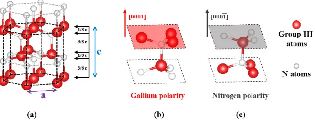
I.3.2 Crystalline structures
The III-nitride materials, such as GaN, AlN, InN and their ternary and quaternary alloys share three distinctive crystal structures, which are rock-salt, zinc-blende and wurtzite. The rock-salt structure, pictured in Figure 1 a, can be obtained at very high pressure conditions, thanks to the reduction of the lattice dimensions, which causes inter-ionic coulomb interaction to favor ionicity over covalent nature [22]. However, the rock-salt structure is a non-compatible structure for industrial applications, as it cannot be obtained by any epitaxial growth. Another crystal structure for III-N materials is the zinc-blende structure, pictured in Figure 1 b, this structure is composed of two interpenetrating face-centered cubic sublattices displaced by one quarter of a body diagonal. However, this crystal structure is less thermodynamically stable under ambient conditions than the wurtzite structure, pictured in Figure 1 c, meaning that the wurtzite structure is typically preferred [23]. We note that for Al, Ga, and In elements, we have electronegativity values of 1.61,
Chapter I: Nitride semiconductors
-6- 1.81, and 1.78 respectively. On the other hand, for N atoms, we have a higher electronegativity value of 3.04, compared to the metal elements. [24]
Figure 1: Illustration of a) rock-salt b) zinc-blende and c) wurtzite crystal structures.
The wurtzite crystalline structure consists of two interpenetrating hexagonal lattices, as shown in Figure 2a. One lattice containing group III atoms and the other N atoms, interpenetrated and shifted by u = 3/8.c along the c-axis, with respect to each other. u is the length of the anion-cation bond and c is the height of the elementary lattice.
We can notice from this figure that the wurtzite crystal structure shows non-symmetry along the c-axis, e.g. the [0001] direction. Thus, [0001] and [0001̅] directions are not equivalent. Therefore, this leads to two different faces of GaN.
The Ga-face (in the [0001] direction) and the N-face (in the [0001̅] direction), shown in Figure 2b and 2c, which corresponds to gallium polarity and nitrogen polarity, respectively.
Chapter I: Nitride semiconductors
-7-
Figure 2: a) III-N wurtzite crystal structure showing the two interpenetrating hexagonal lattices. b) crystallographic orientation [0001] and c) [0001̅] as a function of gallium and nitrogen polarity.
It is important to note that surface polarity strongly affects the final chemical, morphological, and electrical properties of the grown GaN surface templates. We note that these two different surface polarities can be obtained using specific growth conditions.
A gallium surface polarity results in a smooth GaN surface morphology in typical growth conditions for MOVPE, while nitrogen surface polarity tends to a higher surface roughness. This is one of the main reasons for the initial development of LEDs, LDs, and HEMT devices on Ga-polar GaN templates.
However, recently, N-polar GaN templates have shown an increased attention, thanks to alternative device geometries which can be obtained from the flipped spontaneous and piezoelectric polarizations.
In the next paragraphs, we will discuss the different type of polarizations presented within the wurtzite crystalline structure and their origin.
I.3.3 Spontaneous polarization
As previously discussed, GaN material grown in the wurtzite structure is asymmetric along the c-axis, and, as mentioned, nitrogen electronegativity is high compared to that of group III atoms [24]. Together these properties lead to the creation of an electric dipole
Chapter I: Nitride semiconductors
-8- moment directed towards the metal atom along the tetrahedron bonds of the wurtzite structure as pictured in Figure 3a.
Each tetrahedron has an elementary dipole created by the non-superposition of the barycenter of the negative charges with that of the positive charges. These dipoles are added up to produce a macroscopic spontaneous polarization directed along the growth axis of the material, as can be seen from Figure 3b. This effect is called spontaneous polarization (Psp) as it occurs at equilibrium stage independently of the material stress state.
Figure 3: a) Tetrahedron bonding showing dipolar moments and spontaneous polarizations. b) Macroscopic spontaneous polarization and charge repartition at the interfaces of c-axis metal-face of III-N structure.
The spontaneous polarization values of GaN, AlN, and InN are respectively -0.029 C.m-2, -0.081 C.m-2, and -0.032 C.m-2 [25]. The negative Psp sign indicates that the
polarization vector is oriented in the opposite direction to the direction of growth [0001]. According to Vegard’s law, the spontaneous polarization in a AXB1-XD ternary and
AXBXC1-X-YD quaternary alloys can be determined as follows:
Chapter I: Nitride semiconductors
-9-
𝑃𝑠𝑝,𝐴𝑋𝐵𝑌𝐶1−𝑋−𝑌𝐷(𝑋, 𝑌) = 𝑃𝑠𝑝,𝐴𝐷𝑋 + 𝑃𝑠𝑝,𝐵𝐷𝑌 + 𝑃𝑠𝑝,𝐶𝐷(1 − 𝑋 − 𝑌) Eq. 2
Thus, the spontaneous polarization in AlxGa1-xN and AlxIn1-xN ternary alloys, is
obtained as the following:
𝑃𝑠𝑝,𝐴𝑙𝑋𝐺𝑎1−𝑋𝑁(𝑋) = −0.052𝑋 − 0.029 𝐶. 𝑚
−2 Eq. 3
𝑃𝑠𝑝,𝐴𝑙𝑋𝐼𝑛1−𝑋𝑁(𝑋) = −0.049𝑋 − 0.032 𝐶. 𝑚
−2 Eq. 4
Figure 4a shows a visualization of equations number 3 and 4, and we note that the spontaneous polarization of AlxGa1-xN and AlxIn1-xN ternary alloys is always higher than
that for a pure GaN layer.
Figure 4: a) Spontaneous polarization as a function of Al ratio in wurtzite III-N ternary alloys. b) Evolution of the band gap energy of III-N alloys depending on the lattice parameter.
I.3.4 Piezoelectric polarization
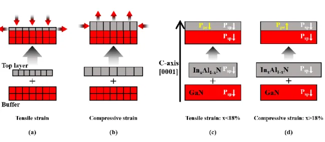
Another component adding to the total polarization within the III-N heterostructure is the piezoelectric polarization (Ppe). In hetero-structures, such as InGaN, AlGaN or InAlN on
GaN, the piezoelectric polarization arises from the strain associated with the lattice mismatch between the top layer and the buffer layer which will form the channel. Strain can be either tensile or compressive, as can be seen from Figure 5a and b.
Chapter I: Nitride semiconductors
-10- When the top layer has a smaller in-plane lattice parameter than the buffer layer, the strain is tensile; and vice versa for the compressive strain. III-N binaries lattice parameter values are shown in Table 2.
Lattice parameter values, for ternary AxB1-xN alloys such as InAlN, AlGaN and
InGaN, can be calculated as follows:
𝑎𝐴𝑋𝐵1−𝑋𝑁(𝑋) = 𝑎𝐴𝑁𝑋 + (1 − 𝑋)𝑎𝐵𝑁 Eq. 5
𝑐𝐴𝑋𝐵1−𝑋𝑁(𝑋) = 𝑐𝐴𝑁𝑋 + (1 − 𝑋)𝑐𝐵𝑁 Eq. 6
We note that AlGaN barriers, when grown under critical thickness, will always be in tensile strain state on GaN buffers. However, this is not the case for InAlN alloys, where the strain state can go from tensile when In% is lower than ~18%, to compressive when In% is higher than ~18%, as shown in Figure 5c and d respectively, and almost null when In% is around 18%, means when InAlN is lattice matched to GaN buffer.
Figure 5: Illustration of a) tensile and b) compressive strains. c) InAlN/GaN strained heterostructure and d) compressed heterostructure.
This piezoelectric polarization is defined in the three dimensional Cartesian coordinate system as a function of the piezoelectric constants eij and the strain field components εj:
Chapter I: Nitride semiconductors
-11- Due to crystal symmetry in wurtzite crystal structure, there are only three independent piezoelectric constants e15, e31, and e33. Values are summarized in Table 2.
Thus, we have: 𝑃𝑝𝑒 = ( 0 0 0 0 𝑒15 0 0 0 0 𝑒15 0 0 𝑒31 𝑒31 𝑒33 0 0 0 ) ∗ ( 𝜀1 𝜀2 𝜀3 𝜀4 𝜀5 𝜀6) Eq. 8
We note that the deformation along the C-axis is εz = (c-c0)/c0, and the deformation in
the perpendicular plane to the C-axis is εx = εy = (a-a0)/a0, where c0 and a0 are respectively
the in-plane and out-of-plane lattice parameters of a fully relaxed bulk material.
According to Hooke’s law, i.e. for elastic deformation that is to say for small deformation, the stress σij is related to the strain ε by:
𝜎𝑖= ∑𝐶𝑖𝑗𝜀𝑗 Eq. 9
Where Cij is the elastic constant or stiffness tensor, which contains five independent
coefficients. Values are summarized in Table 2.
Due to the hexagonal symmetry presented in the wurtzite crystal structure we have:
𝐶𝑖𝑗 = ( 𝐶11 𝐶12 𝐶13 0 0 0 𝐶12 𝐶11 𝐶13 0 0 0 𝐶13 𝐶13 𝐶33 0 0 0 0 0 0 𝐶44 0 0 0 0 0 0 𝐶44 0 0 0 0 0 0 (1 2(𝐶11− 𝐶12))) Eq. 10
Now, as we are growing in the C-axis direction, there is no stress along this axis, and the in-plane stress is uniform (σx = σy). Thus, in this biaxial stress configuration, Eq. 9
becomes:
𝜀𝑥= 𝜀𝑦 ; 𝜀𝑧= −2 ( 𝐶13
Chapter I: Nitride semiconductors
-12- Combining Eq. 8 and Eq. 11, with the fact that εz = (c-c0)/c and εx = εy = (a-a0)/a0 we
find that the strain-induced piezoelectric polarization magnitude value along the C-axis direction is as follows: 𝑃𝑝𝑒 = 2 𝑎−𝑎0 𝑎0 (𝑒31− 𝑒33( 𝐶13 𝐶33)) Eq. 12
We note that, spontaneous and piezoelectric polarizations are in the same direction as each other for tensile strain and in opposite directions for compressive strain, as can be seen from Figure 5c and d.
Wurtzite AlN GaN InN
Eg (eV) a (Å) 6.2 3.111 3.39 3.189 0.7 3.545 c (Å) Psp (C.m-2) e15 (C.m-2) e31 (C.m-2) e33 (C.m-2) C11 (GPa) C12 (GPa) C13 (GPa) C33 (GPa) C44 (GPa) 4.979 -0.081 -0.48 -0.58 1.55 410 149 99 389 125 5.178 -0.029 -0.30 -0.33 0.65 390 145 106 398 105 5.703 -0.032 -0.57 0.97 190 104 121 182 10
Table 2: Different properties of III-Nitride binaries wurtzite crystal: bandgap energy and lattice parameter at 300K, spontaneous, piezoelectric, and elastic parameters. [1, 2, 3, 25, 26, 27, 28, 29, 30, 31] [32]
Typically, AlGaN alloys with Al% around 25%, are used as barriers for GaN-based HEMT heterostructures. However, when growing AlGaN with Al% higher than 25-30%, which is desirable for increased spontaneous polarization, a larger lattice mismatch between AlGaN barrier and GaN buffer occurs, as can be seen from Figure 4b, and this will increase the risk of strain relaxation by cracking [33]. This relaxation results in degraded AlGaN barrier quality, leading to reduced carrier mobility. This relaxation can also raise concerns about the reliability of AlGaN/GaN devices [34].
Chapter I: Nitride semiconductors
-13- As an alternative to AlGaN barriers, the implementation of InAlN barriers with In% around 18%, allows the strain to be controlled in the InAlN/GaN heterostructure, as InAlN barrier lattice parameter will be perfectly matched to that of GaN buffer layer, this can be seen from Figure 4b. Also, we can benefit from the stronger spontaneous polarization shown in Figure 4a. [35]
The realization of a strain-free heterostructures with InAlN/GaN heterostructure is actually an excellent choice since it will lead to a very low Rsheet value [36]. This is the main reason why in this thesis we are interested in growing such material.
I.3.5 Polarization induced charge and two-dimensional electron gas
The polarization can increase or decrease within a bilayer, followed by the generation of a fixed two-dimensional polarization charge density at the abrupt interface of the barrier/channel heterostructure. It is defined as follows: [37]𝜎𝑖𝑛𝑡𝑒𝑟𝑓𝑎𝑐𝑒 = 𝑃(𝑏𝑢𝑓𝑓𝑒𝑟) − 𝑃(𝑏𝑎𝑟𝑟𝑖𝑒𝑟) =
{𝑃𝑠𝑝(𝑏𝑢𝑓𝑓𝑒𝑟)+𝑃𝑝𝑒(𝑏𝑢𝑓𝑓𝑒𝑟)} − {𝑃𝑠𝑝(𝑏𝑎𝑟𝑟𝑖𝑒𝑟)+𝑃𝑝𝑒(𝑏𝑎𝑟𝑟𝑖𝑒𝑟)} Eq. 13
In addition, we have the following two-dimensional polarization charge density on the top layer surface:
𝜎𝐵𝑎𝑟𝑟𝑖𝑒𝑟 𝑠𝑢𝑟𝑓𝑎𝑐𝑒 = 𝑃(𝑏𝑎𝑟𝑟𝑖𝑒𝑟) = 𝑃𝑠𝑝(𝑏𝑎𝑟𝑟𝑖𝑒𝑟) + 𝑃𝑝𝑒(𝑏𝑎𝑟𝑟𝑖𝑒𝑟)} Eq. 14
Respectively, the generated polarization induced sheet charge is denoted as σ/e, where
e = 1.602x10⁻¹⁹ C is the elementary charge of an electron, and σ is the charge density.
In the case of a positive polarization induced bound charge density, e.g. +σ/e, free electrons will tend to compensate the charge, resulting in the formation of the two dimensional electron gas (2DEG) at the abrupt top/bottom interface, as shown in Figure 6a. By analogy, a negative sheet charge density, (-σ/e), can generate a two-dimensional hole gas (2DHG) if the valence band edge crosses the Fermi energy close to the interface. [38]
For AlGaN and InAlN (with Al% > 70%) barriers grown on a Ga-face GaN channel layer, the total polarization induced sheet charge is found to be positive, as can be seen from
Chapter I: Nitride semiconductors
-14- Figure 6 b [38]. This leads as mentioned to the formation of a 2DEG at the barrier/channel interface. We note that, with a lattice matched In0.18Al0.82N layer to GaN, sheet charge
density is almost three times higher than for the conventionally grown Al0.25Ga0.75N barriers
on GaN channels, from which comes the interest of working with InAlN as barriers.
We should note that the 2DEG in III-N heterostructures is realized without any need of a modulation-doped barrier, unlike the 2DEG created in GaAs-based systems where doping is necessary. Yet, the doping in III-N systems can also be performed to enhance carrier density by adjusting the position of the Fermi level.
Figure 6: a) III-N HEMT heterostructure,with the equilibrium band diagram (V = 0 Volts) of the InAlN/GaN heterostructure above b) total polarization induced sheet charge σ/e (Psp+Ppe) bound at the interfaces of Ga-face AlGaN/GaN, AlInN/GaN and InGaN/GaN heterostructures, versus alloy composition of the top layer
[38].
Following this quick theoretical explanation of the polarization-induced charge, now we can predict the sheet carrier concentration of the 2DEG and their dependence on alloy composition for AlGaN/GaN, and InAlN/ GaN (with Al% > 71%) heterostructures.
The sheet electron concentration, ns(x), for undoped pseudomorphic Ga-face AlGaN/GaN or InAlN/GaN HEMT structures, can be approximated by taking advantage of
Chapter I: Nitride semiconductors
-15- the total bound sheet charge σinterface calculated above in Eq. 13, and the following equation: [38]
𝑛𝑠 =𝜎𝑖𝑛𝑡𝑒𝑟𝑓𝑎𝑐𝑒
𝑞 − [
𝜀0𝜀𝑟(𝑥)
𝑡𝑏𝑎𝑟𝑟𝑖𝑒𝑟𝑞2] [𝑞Ø𝑏(𝑥) + 𝐸𝐹(𝑥) − ∆𝐸𝑐] Eq. 15
Where tbarrier is the thickness and εr is the dielectric constant of the barrier layer, q is the elementary charge of the electron. Øb is the height of the Schottky barrier, EF(x) is the position of the Fermi level at the heterointerface with respect to its position in the GaN layer and ∆Ec is the discontinuity of the conduction band at the barrier / GaN interface.
Another intrinsic property of the 2DEG is the electron mobility, µe. As we have seen, the sheet electron concentration in the 2D gas depends mainly on the thickness of the barrier and its alloy composition. In fact, the mobility of electrons depends on numerous elastic and inelastic scattering mechanisms of the carriers on the defects of the structure, such as barrier/channel interface roughness, ionized impurities, threading dislocations, alloy disorder, acoustic and optic phonons. These mechanisms are more or less dominant depending on the temperature and the alloy composition. [39]
I.3.6 Specificities of the III-N elements for electronic applications
By comparing the basic properties of semiconductor materials, we can see the fields of application and the performances accessible by certain alloys. As can be seen in Figure 7, semiconductors differ essentially in the nature and energy of their bandgap. We find among them direct gap materials such as GaAs, InP and III-N alloys such as AlN, GaN and InN. The advantage of this type of bandgap is that the transitions of carriers (electrons or holes) between the energy levels is direct. In this case, radiative recombination or interband absorption is easily generated. These properties are essential in optoelectronic applications based on III-V semiconductors, in particular for the realization of semiconductor lasers.
Chapter I: Nitride semiconductors
-16-
Figure 7: Bandgap energy of different semiconductors depending on the lattice parameter at 300 K.
The energy of the bandgap also plays an important role according to the intended application. Large gap semiconductors can achieve high breakdown voltages and high operating temperatures, making them suitable for use in high voltage supply devices. SiC and GaN have a gap two to three times larger than conventional semiconductors such as Si, GaAs or InP and therefore a breakdown field typically an order of magnitude greater.
Table 3 shows the fundamental properties at 300K of the most important semiconductors for the performance of electronic devices.
Properties AlN GaN InN SiC GaAs InP Si
Bandgap (eV) Breakdown field (MV/cm) Saturation velocity (107cm/s) Electron mobility (cm2/V.s) Relative permittivity (εr) Thermal conductivity (W/cm.K) 6.2 8.4 2.1 135 9.14 2.85 3.39 3.3 2.5 990 9.5 1.3 0.7 1.2 1.8 3.6 15.3 0.45 3.2 3.5 2 650 10 4.5 1.4 0.4 1.2 8500 11.5 0.5 1.3 0.5 1 5400 12.5 0.7 1.1 0.3 1 1500 11.8 1.5
Chapter I: Nitride semiconductors
-17- In general, in order to achieve high current and high frequency operation, high electron mobility (μ) and high electron saturation velocity (νsat) are required. In GaAs, the electron mobility is very high, around 8500 cm2/ (V.s). This is the main reason that field effect transistors (FETs) made with this material have excellent high frequency performance. A major drawback in the fabrication of GaN and SiC-based transistors is the relatively low electron mobility values, which is 990 cm2/ (V.s) for GaN bulk and 650 cm2/ (V.s) for SiC. However, in GaN based HEMT heterostructures, the 2DEG mobility is high compared to the electron mobility in GaN bulk [44], up to 2000 cm²/Vs. This is mainly due to the difference in the carrier diffusion mechanisms between both, HEMTs and bulk. Diffusion mechanisms such as: coulomb collisions, collisions with the crystal lattice, collisions on the surface roughness [45]. In fact, in a HEMT heterostructures, the insertion of AlN spacer reduces alloy disorder at the heterointerface and prevents the diffusion of carriers from the channel to the barrier, resulting in improved carriers mobility. However, these carriers mobility values are sufficient for transistors specifically designed for high power operation.
Another important parameter of semiconductor material is the thermal conductivity (κ). This parameter defines the capacity of heat dissipation by a component. Poor thermal conductivity leads to degraded operation of the device at high temperatures. In general, conventional semiconductors are poor thermal conductors, in particular GaAs and InP. Conversely, AlN, SiC and especially diamond are excellent thermal conductors. GaN is comparable with Si with both having intermediate values.
For a better comparison of the performances of the various semiconductor materials such as GaN, GaAs, Si, and 4H-SiC, several figures of merit have been proposed, as shown in Table 4. These figures combine the main properties of semiconductor materials to classify them according to their performance in power, frequency, and thermal limitation.
The Johnson's figure of merit (JFOM) is a measure of suitability of a semiconductor material for high frequency power transistor applications and requirements. It is the product of the charge carrier saturation velocity in the material and the electric breakdown field under the same conditions. JFOM is given by (Eb.vs/2π)2, where Eb is the semiconductor’s electric
Chapter I: Nitride semiconductors
-18- Keyes's figure of merit (KFOM), considering thermal limitation, provides a thermal limitation to the switching behavior of transistors used in integrated circuits. It is given by
k(c.vs/4π.εs)1/2, where k is the material thermal conductivity, c is light velocity in vacuum, and εs is the material dielectric constant. [47]
Baliga’s figure of merit (BFOM) for power switching, is giving by (εs.µ.Eg3). BOFM defines material parameters to minimize the conduction loss in low-frequency unipolar transistors. Here, µ is the mobility and Eg is the bandgap of the semiconductor. [48]
Baliga also derived a high-frequency figure of merit (BHFFOM) for unipolar switches, giving by µ.Eb2.(VG/4(VB)3)1/2. Here VG is the gate drive voltage and VB is the breakdown
voltage. BHFFOM demonstrates the power loss reduction that can be achieved by a given material. [49]
Si GaAs 4H-SiC GaN
Johnson’s figure of merit JFOM (Eb. vs/2π)2
Keyes’s figure of merit KFOM (k(c.vs/4π.εs)1/2) Baliga’s figure of merit BFOM (εs.µ.Eg3)
Baliga’s figure of merit BHFFOM (µ.Eb2.(VG/4(VB)3)1/2) 1 1 1 1 11 0.45 28 16 410 5.1 290 34 790 1.8 910 100
Table 4: Comparison of normalized figures of merit of various semiconductors. [50] [46] [47] [48] [49]
As can be seen from Table 4, especially in figures of merit of JFOM, BFOM and BHFFOM, it is very clear that GaN is a one of the top choices semiconductors material for high frequency and high power applications compared to the conventional Si, GaAs and SiC materials.
I.4 GaN on Si based electronic applications
Nitride semiconductors have two main fields of application: optoelectronics and high power/ high frequency electronics. For optoelectronics, nitrides have a direct band gap, as already shown in Figure 7, which make them suitable for the realization of optical devices covering a wide range of applications from the near infrared through visible to deep ultraviolet emission and detection. We will not dwell upon this subject since our main center of interest concerns electronic applications.
Chapter I: Nitride semiconductors
-19- Power electronics is the second and the main promising market for GaN-based technologies after LEDs. In particular, GaN is widely used in high frequency devices, and is being developed to replace silicon for high power devices. A comparison of key properties of GaN, GaAs, SiC and silicon is shown in Figure 8. Silicon based devices are limited by an operation frequency of less than 3.5 GHz, as can be seen from Figure 9. In this context, GaAs-based components represented a good alternative to replace silicon technology thanks to their frequency performance. Nevertheless, GaAs technology is penalized in power density because of its weak breakdown field.
Therefore, the development of material-based transistors combining a large gap, a strong breakdown field and a high density of electrons was needed. GaN has a high breakdown field with good thermal conductivity together with the possibility of achieving high mobilities and electronic densities.
Figure 8: Si, SiC, GaAs, GaN capability comparison for electronic applications. [data from Table 3 and Table 1]
Following the early growth of GaN on Si layers of good crystalline quality, the growth of the first high electron mobility transistors (HEMTs) on silicon was demonstrated in the early 2000s [51] [52]. Here again, the main problems come from defects and cracks in the material inducing current leakage and limiting the performance of devices. Techniques for
Chapter I: Nitride semiconductors
-20- stress management and for reducing the density of defects were developed in this area in order to have a better material quality and lower strain, as previously discussed.
Figure 9: Frequency-accessible power ranges for different semiconductor materials reproduced from [53].
Currently, Infineon, Epigan, Macom, ST Mircoelectronics and many other companies are commercializing GaN on Si based devices for high power and high frequency electronics, as they cover a wide range of applications requirements, see Figure 9. Similarly, in 2014 in Grenoble, a young startup, Exagan, started commercializing in this field based on the expertise of CEA-LETI and Soitec.
I.4.1 InAlN/GaN HEMT
Following more than 25 years of development, AlGaN/GaN HEMTs have become the most technologically mature form of GaN-based HEMTs. However, as mentioned in the previous sections, the total strain formed in such heterostructure can create cracks within the material structure, which may limit the device reliability and performance. Another device limitation imposed on AlGaN/GaN based HEMT structures for high frequency performance is the barrier thickness. There is a requirement for thinner top barriers to maintain a favorable channel aspect ratio so as to minimize short-channel effects and enable higher cutoff frequencies. In fact, when AlGaN barrier thickness is below 15 nm, the two-dimensional
![Figure 9: Frequency-accessible power ranges for different semiconductor materials reproduced from [53]](https://thumb-eu.123doks.com/thumbv2/123doknet/12856595.368268/44.892.125.759.210.589/figure-frequency-accessible-ranges-different-semiconductor-materials-reproduced.webp)