HAL Id: hal-01228740
https://hal.archives-ouvertes.fr/hal-01228740
Submitted on 17 Nov 2015
HAL is a multi-disciplinary open access
archive for the deposit and dissemination of
sci-entific research documents, whether they are
pub-lished or not. The documents may come from
teaching and research institutions in France or
abroad, or from public or private research centers.
L’archive ouverte pluridisciplinaire HAL, est
destinée au dépôt et à la diffusion de documents
scientifiques de niveau recherche, publiés ou non,
émanant des établissements d’enseignement et de
recherche français ou étrangers, des laboratoires
publics ou privés.
Monolithic Integrated Reflective Polarization Diversity
SOI-based Slot-Blocker for Fast Reconfigurable 128
Gb/s and 256 Gb/s Optical Networks
G. de Valicourt, S. Chandrasekhar, J. H. Sinsky, C-M. Chang, Y. K. Chen, M.
A. Mestre, Y. Pointurier, Sébastien Bigo, J.-M. Fedeli, Laurent Bramerie, et
al.
To cite this version:
G. de Valicourt, S. Chandrasekhar, J. H. Sinsky, C-M. Chang, Y. K. Chen, et al.. Monolithic Integrated
Reflective Polarization Diversity SOI-based Slot-Blocker for Fast Reconfigurable 128 Gb/s and 256
Gb/s Optical Networks. 41st European Conference on Optical Communication (ECOC 2015), Sep
2015, Valencia, Spain. �10.1109/ECOC.2015.7341953�. �hal-01228740�
Monolithic Integrated Reflective Polarization Diversity
SOI-based Slot-Blocker for Fast Reconfigurable 128 Gb/s and 256
Gb/s Optical Networks
G. de Valicourt(1)*, S. Chandrasekhar(1), J. H. Sinsky(1), C-M. Chang(1), Y. K. Chen(1), M. A. Mestre(2), Y. Pointurier(2), S. Bigo(2), J.-M. Fedeli(3), L. Bramerie(4), J.-C. Simon(4), L. Vivien(5), A. Shen(6), A. Le liepvre(6),
G. H. Duan(6)
(1) Bell Labs, Alcatel-Lucent, 791 Holmdel Road, Holmdel, New Jersey 07733, USA, (2) Alcatel-Lucent Bell Labs, Nozay, France (3) CEA LETI, Minatec, Grenoble, France. (4) Université Européenne de Bretagne, Lannion, France (5) Institut d’Electronique Fondamentale, Orsay, France. (6) III-V Lab, Palaiseau, France *guilhem.de_valicourt@alcatel-lucent.com
Abstract We demonstrate a novel fully integrated, silicon-on-insulator, 16-channel polarization diversity
fast reflective slot-blocker, which contains more than 65 integrated functional elements with nanosecond switching time. We assess its suitability for metropolitan networks with reconfigurable connections.
Introduction
Today’s packet Ethernet metropolitan networks are either very static and highly over-provisioned or require many optoelectronic conversions and electronic switching hardware. Elastic optical network (EON)1 as well as optical packet switching (OPS)2 has been proposed for next-generation of ultrafast, energy- and resource-efficient data transport systems with fast reconfigurable connections. In both proposals, one common implementation is based on wavelength-blocker (WB) technology with broadcast & select approach. The WB or slot-blocker (SB: fast WB) is one of the main building blocks, however, its cost remains high when implemented with discrete components. Photonic integrated circuits (PICs) are expected to provide large cost savings and silicon photonics is a promising option providing large-scale integration of photonic components with high-volume manufacturing compatibility. Integration of silicon-based variable optical attenuator (VOA) combined with silica arrayed waveguide grating (AWG)3 or III-V on silicon semiconductor optical amplifier (SOA) with silicon-on-insulator (SOI)-based AWG4,5 was proposed in order to build 1xN switching fabrics (with N+1
ports). However, a low-port-count package is desirable to overcome cost barriers in PIC module packaging. In addition, SOI-based integration of the AWGs and VOAs is more promising for the co-integration of the photonics and electronics on the same circuit in the future. Recently, we reported a first SOI-based monolithically integrated slot-blocker in a 2-port package6. However, only single polarization (SP) devices were realized and an extinction ratio (ER) no larger than 10 dB was obtained, thereby limiting the blocking/adding functionalities to 80 Gb/s SP-QPSK optical channels.
In this paper, we propose and demonstrate a 16-channel monolithic integrated silicon-based reflective dual-polarization slot-blocker (R-DP-SB) with only a 1-port package. The integrated device performs polarization and wavelength demultiplexing with sub-wavelength switching capability. The reflective-based design shows an ER improvement up to 6 dB compared to our SP device6, compact footprint (1.7 x 3.9 mm2) and fast switching capability (< 10 ns). We demonstrate an add/drop operation at a record 256 Gb/s line rate per channel for monolithic SOI-based SB.
Device design and experimental set-up
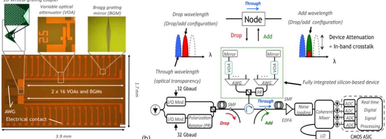
(a) (b)
The compact silicon photonic circuit integrating one double polarization grating coupler (DPGC), two AWGs (200 GHz channel spacing), 32 high-speed VOAs and 32 large-band Bragg grating mirrors (BGMs) was designed and fabricated. Fig. 1 (a) shows a photograph of the PIC. The size of the full circuit was 1.7 × 3.9 mm2, making it the smallest reported 200Gb/s-capable integrated 16-channel slot blocker. For the first time, our reflective configuration allows for a 1-port packaging solution. The fabrication process was similar to the one detailed in our recent paper6. At the input/output of component, light is split/combined into two orthogonal polarization components using the DPGC. Each component is aligned with the TE mode of two identical PICs, side-by-side on the same chip. Polarization independent operation can be achieved by synchronously driving the two PICs. The coupling efficiency of the DPGC with a single mode fiber was around 6 dB and the polarization dependent loss (PDL) around 0.5 dB. The total insertion loss is around 22 dB, which can easily be compensated with an Erbium Doped Fiber Amplifier. The experimental set-up is represented in Fig. 1(b). We used a commercial format and rate adaptable coherent transponder to generate and detect PDM-QPSK or PDM-16QAM modulation formats at 128 Gb/s or 256 Gb/s [each at 32 Gbaud that includes 28% overhead for soft-decision (SD)-forward error correction (FEC)], respectively. The transmitter had a tunable laser and the modulation format was spectrally shaped with a root-raised-cosine roll-off factor of 0.4. An optical circulator is used to direct incoming signals towards our single input/output-port integrated R-DP-SB, and outgoing selected
channels from the device towards following nodes. A VOA and a noise loading stage were placed before the coherent receiver to adjust the optical signal-to-noise ratio (OSNR) level and the optical power of received signal. Received data was processed in real-time using the commercial coherent receiver.
Device characteristics
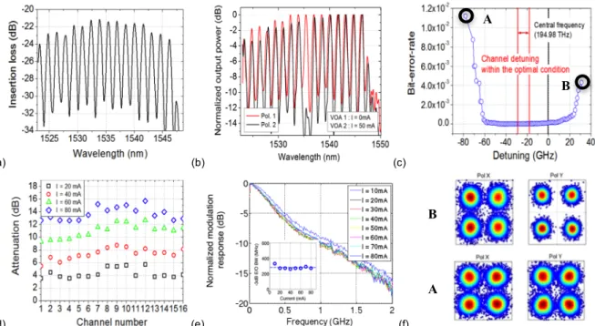
The passband output spectra of all 16 channels are plotted in Fig. 2(a) when injecting a dual-orthogonal-polarized signal. The AWG was designed with 200 GHz spacing from 1523.3 to 1546.2 nm. The excursion of insertion loss across the spectrum is found to be 2.7 dB. Then we excite the R-DP-SB along one specific polarization using a polarization controller. We turn on only the VOA corresponding to one optical path in order to align the polarization with one of the two PICs. The maximum measured PDL of the entire device is around 1.5 dB, which can be compensated by the VOAs at each polarization. Fig. 2(b) reveals a small mismatch between the two AWGs inducing polarization-dependent wavelength shift. We inject a PDM-QSPK signal and detune its frequency respect to the AWG-channel central frequency when passing passively through the device (that we label as “Through”). The pre-FEC bit error rate (BER) is shown in Fig. 2(c) for a fixed signal OSNR of 19.5 dB in 0.1 nm. When the channel frequency is detuned beyond +20-GHz, an error floor is observed at a BER of 4.5x10⁻³ due the severe degradation of one polarization [Fig. 2(f-B)], which is not observed when detuned beyond -60-GHz [Fig. 2(f-A)]. However, the overall transfer function exhibits a large flat region in the center with a 3-dB bandwidth of more than 85 GHz allowing device
(a) (b) (c)
(d) (e) (f)
Fig. 2: Output spectra when injecting (a) two orthogonal polarizations combined (b) one single polarization at a time (superposed). (c) BER penalty for carrier detuning of 128 Gb/s PDM-QPSK signal. (d) Attenuation and (e) modulation response of a VOA depending on the injected current. (f) PDM-QPSK constellations illustrating the impact of the
polarization-dependent wavelength shift of the two AWGs.
z A
B
A B
operations within the optimal conditions. Then the two p-i-n VOAs corresponding to each channel were forward-biased. Fig. 2(d) shows the attenuation as a function of the injected current for all channels. A static ER up to 15.9 dB across the set of gates was measured for 80 mA bias current (with a minimum of 12.6 dB). Further ER improvements are expected by increasing the VOA section length and the doping level. Then a small signal modulation was applied to the VOA in order to determine the electro-optic (E/O) modulation bandwidth. The E/O modulation response is shown in Fig. 2(e) for several biases current. The -3dB E/O bandwidth is constant over the full-injected current range and measured to be 280 MHz [Inset of Fig 2(e)]. The measurement confirms the 10%-90% rise/fall time is less than 10 ns, in agreement with results reported in6 made on a similar VOA structure.
System performances
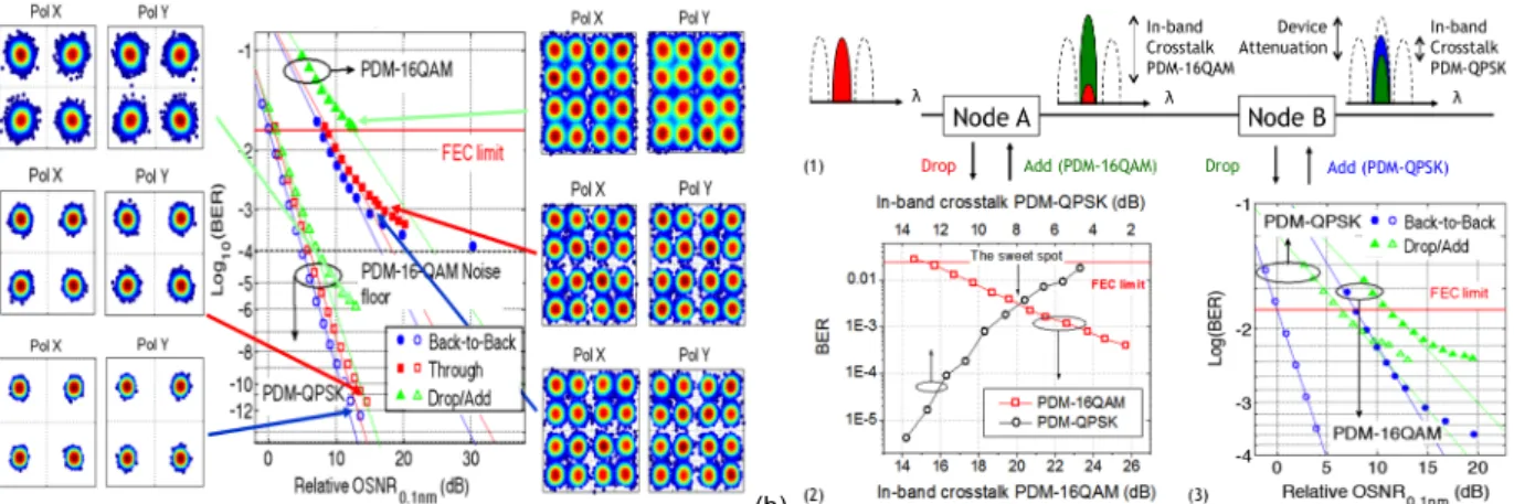
Fig. 3(a) show the results of the transmission experiment in terms of BER versus the relative OSNR in 0.1 nm for 128 Gb/s PDM-QPSK and 256 Gb/s PDM-16-QAM signals in back-to-back, through or drop/add operations. Notice that during drop/add operation we measure the added channel after blocking the dropped channel (which residual creates in-band crosstalk). The back-to-back OSNR corresponding to the BER at the FEC threshold for PDM-QPSK is used as a reference and set to 0dB, and all other OSNR measurements are plotted relative to this reference. Insets in Fig. 3(a) show six exemplary constellations. In all cases, both polarizations are well recovered confirming the polarization diversity scheme of our device. All PDM-QPSK measurements show performances well below the 1.5x10⁻² BER limit (SD-FEC threshold). Less than 1-dB OSNR penalty was measured when dropping and adding PDM-QPSK format. In contrast, PDM-16QAM, though providing increased data rate up to 256 Gb/s, is also more sensitive to in-band crosstalk. Under “Through” operation, less than 0.5dB OSNR penalty was measured. However, when dropping
and adding a new channel, an OSNR penalty of around 5 dB is observed at the FEC-limit. To cope with this penalty, optical power management rules have been investigated7. These rules suggest adjusting the channel power level as a function of the modulation format to maximize performance. Such power management leads to a trade-off between decreasing the in-band crosstalk for the added channel at node A (PDM-16QAM) meanwhile increasing it for the added channel at node B (PDM-QPSK) [Fig. 3(b)(1)]. We studied the impact of the power management on the BER evolution [Fig. 3 (b)(2)]. By increasing the optical power of the added channel in node A, the BER for PDM-16QAM is improved and former values below the FEC limit are achieved. On the contrary, the BER for the PDM-QPSK is degraded and moves closer to the FEC limit. A sweet spot can be defined when both curves intercept. Under such a scenario, we measured the BER as a function of the relative ONSR and the results are shown in Fig. 3(b)(3). Both signals show performances well below the SD-FEC limit. The ONSR penalty for PDM-QPSK is increased to 6.2 dB meanwhile that for the PDM-16QAM is reduced to 3.5 dB.
Conclusions
We have demonstrated the first 1-port package fully integrated silicon-photonics-based fast polarization diversity reflective-slot-blocker including 2 AWGs, 32 VOAs, 32 BRMs and one DPGC. We investigated the performance of this DP-R-SB in an optical network testbed with 128 Gb/s PDM-QPSK and 256 Gb/s PDM-16QAM signals and demonstrated its functionality for reconfigurable optical network.
References
[1] Y. Yoshida et al., Proc. OFC’14, Th5A.2, (2014).
[2] D. Chiaroni, et al., Bell Labs Tech. J., vol. 14, no. 4, (2010). [3] H. Nishi et al., Proc. ECOC, paper We.8.E.3 (2010). [4] G. de Valicourt et al., Photo. Technol. Lett., vol. 26, no. 7
(2014).
[5] O.Raz, et al., Proc. OFC’13, PDP5C.2, (2013).
[6] G. de Valicourt et al., Proc. ECOC’14, We.3.5.5 (2014).
[7] O. Rival et al., J. of Ligthwave Techno., Vol. 29, No. 9 (2011).
(a) (b)
Fig. 3: Experimental results of BER with respect (a) to the relative OSNR in Back-to-Back, through and add/drop configurations, (b(1)) Schematic of optical power management scenario. Experimental results of BER with respect (b(2)) to the In-band crosstalk and