HAL Id: hal-01108922
https://hal.archives-ouvertes.fr/hal-01108922
Submitted on 25 Jan 2015HAL is a multi-disciplinary open access
archive for the deposit and dissemination of sci-entific research documents, whether they are pub-lished or not. The documents may come from teaching and research institutions in France or abroad, or from public or private research centers.
L’archive ouverte pluridisciplinaire HAL, est destinée au dépôt et à la diffusion de documents scientifiques de niveau recherche, publiés ou non, émanant des établissements d’enseignement et de recherche français ou étrangers, des laboratoires publics ou privés.
P-doped region below the AlGaN/GaN interface for
normally-off HEMT
Saleem Hamady, Frédéric Morancho, Bilal Beydoun, Patrick Austin, Mathieu
Gavelle
To cite this version:
Saleem Hamady, Frédéric Morancho, Bilal Beydoun, Patrick Austin, Mathieu Gavelle. P-doped region below the AlGaN/GaN interface for normally-off HEMT. 16th Conference on Power Elec-tronics and Applications, EPE’14-ECCE Europe, Aug 2014, Lappeenranta, Finland. pp.1 - 8, �10.1109/EPE.2014.6910769�. �hal-01108922�
P-Doped Region below the AlGaN/GaN Interface for Normally-Off HEMT
Saleem Hamady
1,2,4, FrédéricMorancho
1,3, Bilal Beydoun
4,Patrick Austin
1,3, Mathieu Gavelle
51
CNRS, LAAS, 7 avenue du colonel Roche, F-31400 Toulouse, France
2Univ de Toulouse, LAAS, F-31400 Toulouse, France
3
Univ de Toulouse, UPS, LAAS, F-31400 Toulouse, France
4GET/LPE, Lebanese University, Hadath campus, Beirut, Lebanon
5
CEA Tech Midi-Pyrénées, 2 Avenue Édouard Belin F31055 Toulouse Cedex 4, France
Tel.: +961 (3) 011338, +33 5 61336488, +961 (3) 754 353,
E-Mail: shamady@laas.fr, morancho@laas.fr, bilbey@ul.edu.lb,austin@laas.fr,
mathieu.gavelle@cea.fr
URL: www.laas.fr,www.univ-tlse3.fr, www.ul.edu.lb
Acknowledgements
This work was funded by the Laboratory for Analysis and Architecture of Systems (LAAS-CNRS/France) and by GET/EDST/UL- AZM & SAADA association.
Keywords
«High electron mobility transistor (HEMT) », «Gallium Nitride (GaN)», «Wide bandgap devices », «Device simulation»
Abstract
Development of a new design for enhancement-mode AlGaN/GaN HEMT is presented. The normally-off operation was achieved by burying a p-GaN region below the AlGaN/GaN interface only below the gate. Simulation results show that the proposed technique is capable of shifting the threshold voltage to positive values, making the HEMT normally-off. To address the advantages and drawbacks of the proposed structure a comparison with the normally-off Gate injection transistor (GIT) was performed. The proposed structure seems to be more effective when it comes to the p-doping concentration required to achieve normally-off operation and offers superior confinement for the two dimensional electron gas. On the other hand, the low forward gate voltage limits the increase of the threshold voltage.
Introduction
AlGaN/GaN HEMTs are very promising candidates for high frequency applications with high power and low noise, such as microwave and millimeter wave communications, imaging and radars [1]. With the high field strength offered by GaN and the high mobility of the two-dimensional-electron-gas (2DEG) presented in the HEMT, this device can attain high breakdown voltage with low on state resistance and high switching frequency, surpassing the limitation of conventional silicon devices. While power switching applications strongly demand normally-off operation [2], conventional HEMTs attain a channel populated with electrons at zero gate voltage making them normally-on. Several normally-off structures have been proposed such as recessed gate structures [3], fluorine ion treatment [4], pn junction gate structures [5], thin AlGaN barrier [6], AlN/GaN structure [7] and Gate injection transistor [8].
The effectiveness of the agent used to obtain normally-off, whether it's recessing the gate, introducing a cap layer or implanting fluorine, increases as the agent come closer to the AlGaN/GaN interface. Unfortunately, in introducing a cap layer or recessing the gate, coming closer to the interface means decreasing the barrier thickness which strongly affect the density of the 2DEG.
In the case of fluorine implantation, getting closer to the interface increases the probability of fluorine ions getting into the channel and hence the degradation of the mobility of the 2DEG [9]. In this work, normally-off operation is achieved by introducing a p-doped region in the unintentionally doped (UID) GaN layer, below the AlGaN/GaN interface, only under the gate electrode. Using this approach, the agent (p-doped region) can approach the AlGaN/GaN interface without affecting the thickness of the barrier.
Simulation Strategy
To do this study, ATLAS, a physically-based TCAD simulation tool from Silvaco, was used. Physical models used in the simulation include Shockley-Read Hall recombination, Fermi-Dirac statistics and field-dependent mobility [10]. The simulator was calibrated using a normally-on HEMT device shown in figure 1.
To match the simulated threshold voltage (Vth), transconductance and the off-state current with the ones experimentally measured (see figure 2), the energy and the concentration of the acceptor traps, as well as the density of the two dimensional electron gas, were tuned. Some of the parameters used during the simulation are shown in Table 1.
Fig: 2: Comparison of the experimental and simulated Id (Vgs) transfer characteristics of the conventional normally-on HEMT: fitting the simulated threshold voltage, transconductance and off
state current to the ones experimentally measured.
0.01 0.1 1 10 100 -6 -5 -4 -3 -2 -1 0 1 2 Dra in curr ent Id (m A/m m)
Gate to Source voltage Vgs (V)
Simulation Experiment
Fig. 1: Schematic cross section of the normally-on HEMT used to calibrate the simulator. 2 µm Drain Silicon UID-GaN – Doping : 1016 cm-3 1.1 µm 30 nm 2 µm Gate Source 2 µm 5 µm 2 µm Air Air Al0.25GaN – Doping : 1015 cm-3 30 nm
The schematic cross-section of the proposed normally-off HEMT design is shown in figure 3. The localized p-GaN region has been previously created by other groups using Mg ion implantation to create the current blocking layer (CBL) in AlGaN/GaN current aperture vertical electron transistors (CAVET) [11].
The thickness and width of the P-GaN region are 100 nm and 1μm respectively. The distance between the AlGaN/GaN interface and the top of the p-GaN region is equal to 10 nm. The doping concentration of the p-GaN region will be increased until normally-off operation is achieved. To point out the advantages and drawbacks of the proposed structure, it will then be compared to the normally-off Gate Injection Transistor (GIT).
Results and discussion
HEMT with a buried p-GaN region:
Figure 4 shows the shift in the threshold voltage due to the introduction of the p-GaN region. It is clear that the threshold voltage increase with increasing the p-doping concentration to reach 0.5 V at a doping concentration of 2.5 × 1018 cm-3. To explain this shift, the band diagram, along CUT in figure 3, is shown in figure 5. It is well known that, in p-type semiconductors, the Fermi level shifts towards the valence band. However, since at equilibrium the Fermi level is constant, this shift will manifest itself through uplifting the conduction band. The uplift of the conduction band in the p-doped region will elevate the triangular well at the AlGaN/GaN interface. The elevation of the triangular well with respect to the Fermi level causes the shift in the threshold voltage. However, if the uplift in the p-doped region is insufficient to elevate the triangular well above the Fermi level the HEMT remains normally-on (p-doping < 2× 1018 cm-3).
Fig. 3: Schematic cross-section of the HEMT with a buried p-GaN region with some physical and geometrical parameters. Drain Silicon UID-GaN 1.1 µm 30 nm 2 µm Gate Source 2 µm 5 µm 2 µm 2 µm Air Air P-GaN UID-GaN 10 nm 1μm 100 nm Al0.25GaN CUT 30 nm
Table I: Parameters used during simulation
Parameter Value
Band offset 0.7 ( Eg (AlxGaN) - Eg (GaN)) [eV]
x-mole fraction of Aluminum in AlGaN "x" 0.25 - 0.18
Band Gap of AlxGaN 6.2 x + 3.4 (1-x) - 1.3 x (1 - x ) [eV] Dielectric Constant of AlxGaN 9.5 - 0.5 x [eV]
Interfacial charge density K ( PGaN - PAlxGaN) / q [cm-2]
To examine the off-state current and the breakdown voltage, the structure shown in figure 6 was studied. However, due to convergence problems at high voltages in the normally-off HEMT with high fluorine concentrations, a smaller x-mole fraction of 0.15 was used instead. In this case, a smaller doping concentration of 5 × 1017 cm-3 is needed to achieve normally-off operation with a threshold voltage of 0.5 V. (more details are shown in the coming section)
Figure 5 shows the variation of the drain current with the applied drain to source voltage Id(Vds). In order to study the two HEMTs in the off-state, i.e. below their threshold voltage, the applied gate to source voltage is: Vgs = Vth - 1 V.
It is clear that neither the vertical breakdown voltage, nor the off-state current are affected by the implanted fluorine ions. A breakdown voltage of 280 V was obtained in both cases.
Fig. 5: Conduction band along CUT - see figure 3 - at various p-doping concentrations showing the uplifting of the triangular well above the Fermi level for doping concentrations higher than 2×1018 cm-3
-0.5 0 0.5 1 1.5 2 2.5 3 3.5 4 0.17 0.2 0.23 0.26 0.29 0.32 0.35 0.38 Co n du ct io n ba n d (e V) Depth (µm) w/o P-GaN 5 10¹⁷ 10¹⁸ 2 10¹⁸ 2.5 10¹⁸ Fermi Level P-doping concentration (cm-3) P - GaN Gat e AlGaN UID
-GaN UID - GaN
Fig. 4: The increase of the threshold voltage with the doping concentration due to the buried p-GaN region. Normally-off operation with Vth=0.5 is achieved at a p-doping concentration of 2.5 ×1018 cm-3
0 0.002 0.004 0.006 0.008 0.01 -5 -4 -3 -2 -1 0 1 D ra in C ur re nt Id (A /m m )
Gate to Source Voltage Vgs(V)
w/o P-GaN 5 10¹⁷ 10¹⁸ 2 10¹⁸ 2.5 10¹⁸ P-doping concentration (cm-3)
Comparison between the Gate Injection Transistor and the proposed structure:
A well know normally-off HEMT is the Gate Injection Transistor (GIT). This transistor also utilized a p-region to achieve normally-off operation. However, in the GIT the p-region is introduced above the barrier layer rather than below the channel which is the case in our proposed structure.
In this section a comparison with the GIT is performed aiming to point out the advantages and drawbacks of our proposed structure. In the GIT proposed in [8] the optimized thickness and x-mole fraction of the AlGaN layer are 25 nm and 0.15 respectively. The x-mole fraction of the p-AlGaN cap layer is 0.15.
For a fair comparison between our proposed structure and the GIT, the same physical parameters are used for both structures (thickness and doping of GaN and AlGaN). In both cases, the thickness and width p-GaN region are 100 nm and 1μm respectively. The p-doping concentration will be increased until normally-off operation in both structures is achieved. The chosen “normally-off” criterion is a threshold voltage of 0.5 V.
The schematic cross-section of the simulated normally-off GIT is shown in figure 6. As for our proposed structure the schematic cross-section is the same as the one shown in figure 3 expect for the thickness and x-mole fraction that are reduced to 25 nm and 0.15 respectively.
Fig 6: Schematic cross-section of the simulated gate injection transistor (GIT). This structure is compared to our proposed structure.
2 µm Drain Silicon 1.1 µm 30 nm 2 µm Gate Source 5 µm 2 µm 2 µm Air Air P-AlGaN 100 nm Al0.15GaN CUT 2 25 nm 1μm UID-GaN
Fig. 5: Simulated Id(Vds) characteristics in the off-state, showing the off-state current and the breakdown voltage of the normally-on HEMT and the normally-off HEMT with a buried p-GaN
region. 1E-6 1E-5 1E-4 1E-3 1E-2 0 50 100 150 200 250 300 D ra in C ur re nt (A /m m )
Draint to Source voltage Vds (V) with p-GaN
Figures 7 and 8 show the variation of the threshold voltage and the forward gate voltage of the GIT and our proposed structure respectively. These values are extracted at Vds=1 V.
To achieve a threshold voltage of 0.5 V, a doping concentration of 2×1018 cm-3 is required in the case of GIT while in our proposed structure, only 5×1017 cm-3 is sufficient. Therefore, our proposed structure is more efficient when it comes to doping concentration required to achieve normally-off operation. On the other hand, the forward gate voltage is much higher in the case of the Gate Injection Transistor. This is attributed to the use of p-AlGaN gate in the GIT rather than a Schottky gate. The low forward gate voltage in our proposed structure limits the increase in the threshold voltage to higher values.
To address the quality of the triangular well in which the channel electrons are confined. The band diagram for both structures, along CUT in figure 3 and CUT2 in figure 6, is shown in figure 9. It is clear that the confinement of the 2DEG is superior in our case. This better confinement will lead to higher mobility. However, in our simulation the mobility of the 2DEG, in all cases, was fixed to 1500 cm2/v.sec. This hinders the comparison of the on-state resistance and transconductance for the two structures.
Fig. 8: Threshold voltage and forward gate voltage of the GIT at various doping concentrations. A threshold voltage of 0.5 V was achieved at doping concentration of 5×1017 cm-3 at this doping
concentration the forward gate voltage was 0.8 V. Values are extracted at Vds =1 V -1.5 -1 -0.5 0 0.5 1 1.5 1 2.5E+17 5E+17 Volt age (V) Doping concentration (cm-3) Threshold voltage Forward Gate voltage
Fig. 7: Threshold voltage and forward gate voltage of the GIT at various doping concentrations. A threshold voltage of 0.5 V was achieved at doping concentration of 2×1018 cm-3 at this doping
concentration the forward gate voltage was 5.1 V. Values are extracted at Vds =1 V -3 -2 -1 0 1 2 3 4 5 6
5E+17 1E+18 1.5E+18 2E+18
Vol
tage
(V)
Doping concentration (cm-3)
Threshold voltage Forward Gate voltage
Conclusion
In this work, a new normally-off HEMT design was proposed. In order to achieve normally-off operation, a p-GaN region was introduced below the gate electrode and 10 nm under the AlGaN/GaN interface. After calibrating the simulator using experimental data from a normally-on HEMT, the p-GaN region was introduced. Simulation results have shown that this technique is capable of shifting the threshold voltage to positive values making the HEMT normally-off. When compared to the gate injection transistor, this design is more effective when it comes to the doping concentration required to achieve normally-off operation and offers better confinement to the two dimensional electron gas. On the other hand, the proposed structure attains a low forward gate voltage when compared to the GIT. This low forward gate voltage, which limits the increase in the threshold voltage, can be eliminated by introducing an insulating material under the gate such as Al2O3, SiN or HfO2.
References
[1] K. Bong-Hwan, P. Seoung-Hwan, L. Jung-Hee, and M. Yong-Tae, “Effect of In Composition on Two-Dimensional Electron Gas in Wurtzite AlGaN/InGaN Heterostructures,” Chin. Phys. Lett., vol. 27, no. 11, p. 118501, Nov. 2010.
[2] H. Kambayashi, Y. Satoh, T. Kokawa, N. Ikeda, T. Nomura, and S. Kato, “High field-effect mobility normally-off AlGaN/GaN hybrid MOS-HFET on Si substrate by selective area growth technique,” Solid-State Electron., vol. 56, no. 1, pp. 163–167, Feb. 2011.
[3] S. D. Burnham, K. Boutros, P. Hashimoto, C. Butler, D. W. S. Wong, M. Hu, and M. Micovic, “Gate-recessed normally-off GaN-on- Si HEMT using a new O2-BCl3 digital etching technique,” Phys. Status
Solidi C, vol. 7, no. 7–8, pp. 2010–2012, 2010.
[4] H. Chen, M. Wang, and K. J. Chen, “Self-aligned enhancement-mode AlGaN/GaN HEMTs using 25 keV fluorine ion implantation,” in Device Research Conference (DRC), 2010, 2010, pp. 137–138.
[5] X. Hu, G. Simin, J. Yang, M. A. Khan, R. Gaska, and M. S. Shur, “Enhancement mode AlGaN/GaN HFET with selectively grown pn junction gate,” Electron. Lett., vol. 36, no. 8, pp. 753–754, 2000.
[6] Y. Ohmaki, M. Tanimoto, S. Akamatsu, and T. Mukai, “Enhancement-Mode AlGaN/AlN/GaN High Electron Mobility Transistor with Low On-State Resistance and High Breakdown Voltage,” Jpn. J. Appl. Phys., vol. 45, no. No. 44, pp. L1168–L1170, Nov. 2006.
[7] M. Higashiwaki, T. Mimura, and T. Matsui, “Enhancement-Mode AlN/GaN HFETs Using Cat-CVD SiN,” IEEE Trans. Electron Devices, vol. 54, no. 6, pp. 1566–1570, 2007.
[8] Y. Uemoto, M. Hikita, H. Ueno, H. Matsuo, H. Ishida, M. Yanagihara, T. Ueda, T. Tanaka, and D. Ueda, “Gate Injection Transistor (GIT)- A Normally-Off AlGaN/GaN Power Transistor Using Conductivity Modulation,” IEEE Trans. Electron Devices, vol. 54, no. 12, pp. 3393–3399, 2007.
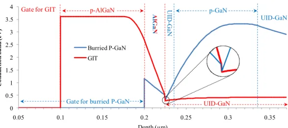
Fig. 9: Band diagram of the gate injection transistor and the HEMT with a buried p-GaN region corresponding to a threshold voltage of 0.5 V with a p-doping concentration of 2 × 1018 cm-3 andof 5×1017 cm-3 respectively. The zoomed part shows a better triangular well in the case of HEMT with
buried p-GaN region
0 0.5 1 1.5 2 2.5 3 3.5 4 0.05 0.1 0.15 0.2 0.25 0.3 0.35 C on du ct io n ba nd (e V ) Depth (µm) Burried P-GaN GIT
Gate for burried P-GaN
Gate for GIT p-AlGaN
UID-GaN p-GaN
UID
[9] K. J. Chen, L. Yuan, M. J. Wang, H. Chen, S. Huang, Q. Zhou, C. Zhou, B. K. Li, and J. N. Wang, “Physics of fluorine plasma ion implantation for GaN normally-off HEMT technology,” in Electron Devices Meeting (IEDM), 2011 IEEE International, 2011, pp. 19–4.
[10] SILVACO, “ATLAS User’s Manual DEVICE SIMULATION SOFTWARE,” Santa Clara, CA,, 2011, pp. 330–331.
[11] S. Chowdhury, B. L. Swenson, and U. K. Mishra, “Enhancement and Depletion Mode AlGaN/GaN CAVET With Mg-Ion-Implanted GaN as Current Blocking Layer,” IEEE Electron Device Lett., vol. 29, no. 6, pp. 543–545, Jun. 2008.