HAL Id: tel-02115340
https://tel.archives-ouvertes.fr/tel-02115340
Submitted on 30 Apr 2019
HAL is a multi-disciplinary open access archive for the deposit and dissemination of sci-entific research documents, whether they are pub-lished or not. The documents may come from teaching and research institutions in France or abroad, or from public or private research centers.
L’archive ouverte pluridisciplinaire HAL, est destinée au dépôt et à la diffusion de documents scientifiques de niveau recherche, publiés ou non, émanant des établissements d’enseignement et de recherche français ou étrangers, des laboratoires publics ou privés.
Low-Temperature process and innovative TFETs
architectures for 3D integration
Carlos Diaz Llorente
To cite this version:
Carlos Diaz Llorente. Characterization of TFETs made using a Low-Temperature process and innova-tive TFETs architectures for 3D integration. Micro and nanotechnologies/Microelectronics. Université Grenoble Alpes, 2018. English. �NNT : 2018GREAT096�. �tel-02115340�
THÈSE
Pour obtenir le grade de
DOCTEUR DE LA COMMUNAUTE UNIVERSITE
GRENOBLE ALPES
Spécialité : Nano Electronique et Nano Technologies
Arrêté ministériel : 25 mai 2016
Présentée par
Carlos DIAZ LLORENTE
Thèse dirigée par Gérard GHIBAUDO, Directeur, CNRS, et codirigée par Cyrille LE ROYER et Jean-Pierre COLINGE, Co-encadrants, CEA/LETI
préparée au sein du Laboratoire CEA/LETI
dans l'École Doctorale Electronique, Electrotechnique, Automatique et Traitement du Signal (EEATS)
Caractérisation de transistors à effet tunnel
fabriqués par un processus basse température et
des architectures innovantes de TFETs pour
l’intégration 3D
Characterization of TFETs made using a Low-Temperature process and innovative TFETs architectures for 3D integration Thèse soutenue publiquement le 27 Novembre 2018,
devant le jury composé de : Mme. Mireille MOUIS
Directeur de recherche, CNRS ALPES (Président)
M. Olivier BONNAUD
Professeur émérite, Université RENNES 1 (Rapporteur)
M. Guilhem LARRIEU
Charge de recherche, CNRS MIDI-PYRENEES (Rapporteur)
M. Francisco GAMIZ
Professeur, Université de Grenade (Examinateur)
M. Gérard GHIBAUDO
Directeur de recherche, CNRS ALPES (Directeur de thèse)
M. Cyrille LE ROYER
Ingénieur de recherche, CEA/LETI (Encadrant)
M. Jean-Pierre COLINGE
Directeur de recherche, CEA/LETI (Co-encadrant)
To my parents, my sister and all members of my family
Acknowledgements
Now that I am done writing my PhD thesis and looking back at the last three years, I can say that my research work at CEA-Leti has been a unique experience. There were many positive aspects, such as being involved in state-of-the-art investigations, meet very nice co-workers always willing to help me, learning French and living in a foreign country. All these helped me to grow as a person. Of course, there were also challenges, but these are intrinsic to the very nature of Research.
First of all, I want to express how very grateful I am to the people that have helped me to carry out my PhD research work and condense the results into this thesis manuscript.
I will start by thanking my CEA supervisor Cyrille Le Royer because, starting from the first day, he provided me a very warm welcome (the two first months in France were particularly difficult for me) and took care of all the procedures needed for welcoming me in the LICL laboratory. He also had the patience to talk to me in English until my French became good enough to meaningful discussions about work. I also want to thank him for teaching me a thorough and accurate method for carrying out research. I also want also to express my gratitude to my thesis director Gérard Ghibaudo for participating in the meetings that changed the orientation of the thesis and indicate which type of experiments could provide a better understanding of the physics at play in the devices I was measuring. My gratitude also goes to Sorin Cristoloveanu, my supervisor at IMEP-LAHC for being actively involved in the thesis, for suggesting many innovative ideas, for all the corrections he made to the papers I wrote, and of course for his great sense of humor. I am also indebted to Jean-Pierre Colinge whom I have to thank a lot for supervising the last year and a half of my thesis. Finally, I want to thank again Jean-Pierre, Sorin and Cyrille for all the corrections they made to this PhD manuscript.
I also want to say a big "thank you" to the team of the LICL laboratory, from the “chef du labo” to the permanents members, and especially to the Post Doc and PhD students: Fabien, Aurore, Loïc, Lina, Giulia, Jessy, Remy, Sotiris, Mathilde, Alex, Vincent, Artemis, Corentin, Benoit, José, Carlos N., Daphnée, Camila, Julien B., Julien D., Claude, Bernard, Laurent, Louis, Claire and François I do not want to forget Sabine, Brigitte and Jumana Boussey, because they were always available to help me with all the sometimes bureaucratic procedures at the CEA and at the doctoral school. I have also to express my gratitude to Sébastien Martinie from LSM laboratory for always being available to discuss the physics of TFETs. Without his help with the simulation decks I would not have been able to obtain such interesting results. I also want to Christoforos Theodorou from IMEP-LAHC for all the days we have spent together carrying out noise measurements and interpreting the results.
Last but not least, I want to thank my parents, sister and the rest of my family for the continuous support they provided during these three years away from home. My biggest thanks go to my parents, whom always encouraged me to continue no matter what was going on.
General Index
Abstract/Résumé ... IX
List of constants, symbols and acronyms ... XI
Introduction ... XV
Bibliography ... XIX
Chapter 1. Context of the thesis and Beyond-CMOS devices ... 1
1.1. The end of planar scaling ... 1
1.2. Towards the path of enhanced power efficiency ... 3
1.2.1. CMOS limitation for low-voltage applications ... 5
1.3. Beyond-CMOS devices ... 7
1.3.1. Impact ionization MOSFET (IMOS) ... 8
1.3.2. Z2-FET ... 9
1.3.3. Negative capacitance FET (NC-FET) ... 10
1.3.4. Nano-electromechanical Switches (NEMS) ... 11
1.3.5. Tunnel FETs (TFETs) ... 12
1.4. Conclusions ... 13
Bibliography ... 14
Chapter 2. Tunnel FET devices ... 17
2.1. Interband tunneling (Esaki diode) ... 17
2.2. Tunnel FET operation ... 19
2.2.1. Simulation TFETs vs. Experimental TFETs ... 22
2.2.2. Trap Assisted Tunneling (TAT) ... 24
2.3. TFET device engineering ... 26
2.3.1. Silicon homojunction TFET... 26
2.3.1.1 Complementary TFET in CMOS Foundry ... 28
2.3.2. TFET optimization ... 29
2.3.2.1 Impact of body thickness ... 30
2.3.2.3 Impact of intrinsic region: Ambipolarity ... 31
2.3.2.4 Impact of Equivalent Oxide Thickness (EOT) ... 32
2.3.2.5 Si TFETs vs. SiGe TFETs ... 33
2.3.3. TFET optimization challenges ... 34
2.4. CEA TFETs: State of the art ... 35
2.4.1. Si1-xGexOI and GeOI TFETs ... 35
2.4.2. Strained TFETs with ultra-thin body ... 36
2.4.3. Nanowire TFETs ... 37
2.5. Ultimate innovative Tunnel TFETs... 38
2.5.1. Strained Si and SiGe GAA nanowire TFET ... 38
2.5.2. Junction TFET and T-Gate Schottky barrier TFET (TSB-TFET) ... 39
2.5.3. Parallel electric field TFET ... 40
2.5.4. III-V based TFETs ... 41
2.5.5. Junctionless TFET ... 42
2.5.6. 2D materials TFETs ... 43
2.6. TFET Benchmark ... 45
2.7. Conclusions ... 47
Bibliography ... 49
Chapter 3. Low-Temperature TFETs ... 55
3.1. Basis of 3D sequential integration ... 55
3.2. Low-temperature TFET process... 56
3.2.1. Process flow ... 56
3.2.2. Focus on PAI and SPER techniques ... 57
3.3. Electrical characterization ... 57
3.3.1. Dual ID-VDS method ... 57
3.3.2. Analysis of the tunneling process ... 59
3.3.3. ID(VG) characteristics ... 60
3.4. Simulation of Low-Temperature TFETs ... 64
3.5. TFET Benchmark comparison ... 66
3.6. Impact of fin width on TFET performance ... 69
3.7. Conclusions ... 73
Chapter 4. Investigation of defects in Tunnel FET devices ... 77
4.1. Introduction ... 77
4.2. Charge Pumping ... 78
4.2.1. Basic principle ... 78
4.2.2. Set up configuration in FDSOI TFETs ... 79
4.2.3. Impact of back-gate voltage on charge pumping current ... 81
4.2.4. Density of interface states for LT and HT TFETs ... 83
4.3. Charge pumping: Density of carriers and ICP current ... 84
4.3.1. Impact of back-gate voltage on density of carriers ... 84
4.3.2. Extraction of defect density at different pulse base levels ... 89
4.3.2.1 Pulse gate base level of - 0.35 V... 90
4.3.2.2 Pulse gate base level of - 0.85 V... 91
4.4. Low-Frequency Noise analysis ... 94
4.4.1. Impact of the process temperature ... 94
4.4.2. Impact of TFET fin width on LFN behavior ... 97
4.4.3. Impact of temperature on TFET LFN ... 98
4.5. Conclusions ... 100
Bibliography ... 102
Chapter 5. Innovative TFET architectures ... 103
5.1. Motivation ... 103
5.2. Proposed TFET architectures ... 104
5.2.1. Extended-Source TFET... 104
5.2.2. Pure Boron TFET ... 105
5.2.3. Sharp Tip TFET ... 107
5.3. Extended-Source TFET ... 108
5.3.1. Impact of the restricted tunneling length for a given Si film thickness ... 108
5.3.2. Impact of Si film thickness for a given restricted tunneling length (Lrt) ... 110
5.3.3. Comparison of Extended-Source TFET with Standard TFET ... 111
5.3.4. Impact of gate length on drive current ... 112
5.4. Pure Boron TFETs ... 113
5.4.1. Impact of silicon body thickness ... 113
5.4.2. Comparison of Pure Boron TFET with Standard TFET ... 115
5.4.3. Impact of gate length on drive current ... 115
5.5. Sharp Tip TFET ... 117
5.5.2. Impact of gate length on drive current ... 118
5.6. SiGe TFETs ... 119
5.6.1. Pure Boron and Standard TFET ... 119
5.6.2. Impact of gate length and body thickness in the drive current ... 121
5.6.3. Impact of gate length for different germanium concentrations ... 122
5.7. Conclusions ... 124
Bibliography ... 126
General conclusions... 129
Author publication list ... 135
Résumé du travail de la thèse en français ... 137
Appendix A. Tunnel FET TCAD simulation ... 149
A.1. Band-To-Band Tunneling... 149
Characterization of TFETs made using a Low-Temperature process and innovative TFETs architectures for 3D integration
This thesis presents a study of FDSOI Tunnel FETs (TFETs) from planar to trigate/nanowire structures. For the first time we report functional “Low-Temperature” (LT) TFETs fabricated with low-thermal budget (630°C) process flow, specifically designed for top tier devices in 3D sequential integration. “Dual IDVDS” method
confirms that these devices are real TFETs and not Schottky FETs. Electrical characterization shows that LT TFETs performance is comparable with “High-Temperature” (HT) TFETs (1050°C). However, LT TFETs exhibit ON-current enhancement, OFF-current degradation and VTH shift with respect to HT TFETs that cannot
be explained via BTBT mechanism. Charge pumping measurements reveal a higher defect density at the top silicon/oxide interface for geometries with narrow widths in LT than HT TFETs. In addition, low-frequency noise analyses shed some light on the nature of these defects. In LT TFETs, we determined a non-uniform distribution of defects at the top surface and also at the tunneling junction that causes trap-assisted tunneling (TAT). TAT is responsible of the current generation that degrades the subthreshold swing. This indicates the tight requirements for quality epitaxy growth and junction optimization in TFETs. Finally, we proposed novel TFET architectures. TCAD study shows that the extension of the source into the body region provides vertical BTBT and a larger tunneling surface. Ultra-thin heavily doped boron layers could allow the possibility to obtain simultaneously a good ON-current and sub-thermal subthreshold slope in TFETs.
Keywords: Tunnel FET, TFET, SOI, BTBT, Low-Temperature, 3D integration, Charge pumping, low-frequency noise, Extended-source, Pure Boron.
Caractérisation de transistors à effet tunnel fabriqués par un processus basse température et des architectures innovantes de TFETs pour l’intégration 3D
Cette thèse porte sur l’étude de transistor à effet tunnel (TFET) en FDSOI à géométries planaire et triple grille/nanofils. Nous rapportons pour la première fois des TFETs fabriqués par un processus basse température (600°C), qui est identique à celui utilisé pour l’intégration monolithique 3D. La méthode “Dual IDVDS” confirme
que ces TFETs fonctionnent par effet tunnel et non pas par effet Schottky. Les résultats des mesures électriques montrent que l’abaissement de la température de fabrication de 1050°C (HT) à 600°C (LT) ne dégrade pas les propriétés des TFETs. Néanmoins, les dispositifs réalisés à basse température montrent un courant de drain et de fuite plus élevés et une tension de seuil différente par rapport aux HT TFETs. Ces phénomènes ne peuvent pas être expliqués par le mécanisme d’effet tunnel. Le courant de pompage de charges révèle une densité d’états d’interface plus grande à l’interface oxide/Si pour les dispositifs LT que dans les TFETs HT pour les zones actives étroites. Par ailleurs, une analyse de bruit basse fréquence permet de mieux comprendre la nature des pièges dans les TFETs LT et HT. Dans les TFETs réalisés à basse température nous avons mis en évidence une concentration en défauts non uniforme à l’interface oxide/Si et à la jonction tunnel qui cause un effet tunnel assisté par piège (TAT). Ce courant TAT est responsable de la dégradation de la pente sous seuil. Ce résultat montre la direction à suivre pour optimiser ces structures, à savoir une épitaxie de très haute qualité et une optimisation fine des jonctions. Finalement, nous avons proposé de nouvelles architectures innovatrices de transistors à effet tunnel. L’étude de simulation TCAD montre que l’extension de la jonction tunnel dans le canal augmente la surface de la région qui engendre le courant BTBT. Une fine couche dopée avec une dose ultra-haute en bore pourrait permettre l’obtention à la fois d’une pente sous le seuil faible et un fort courant ON pour le TFET.
Mots clés: transistor à effet tunnel, TFET, SOI, BTBT, basse température, intégration 3D, pompage de charges, bruit basse fréquence, jonction étendue, Bore.
List of constants, symbols and acronyms
Constant definition magnitude Units
k/kB Boltzmann constant 1.38×10
-23
J·K-1
q Elementary charge 1.602×10⁻¹⁹ C
εSi Si relative permittivity 11.8 dimensionless
h Planck constant 6.626×10⁻³⁴ J·s
Symbol definition Units
A Effective channel area µm2
α Gate activity factor dimensionless
β Inverse of thermal voltage V-1 or mV-1
CD Bulk depletion capacitance F/cm
2
CLOAD Load capacitance F/cm
2 Cox Oxide capacitance F/cm 2 CVDD 2 Switching energy J or eV Dn Electron diffusion cm 2 /s ΔΦ Tunneling window V or eV
ΔVG Amplitude gate pulse V
EC/EV Conduction/Valence band energy eV
EF Energy Fermi level eV
EG/Eg Energy bandgap eV
Emax Maximum electric field V/cm
ET Energy interface state level eV
f Frequency Hz or GHz
felas Elastic force N
felec Electric field-induced force N
ΦF Fermi potential V or eV
ΦG Gate work function eV
fs(E)/ fD(E) Source and drain fermi distributions dimensionless
φs/ΔΦS Electrostatic surface potential V or eV
gm Transconductance A/V
ICP Charge pumping current A
ID Drain/drive/tunneling current µA/µm or A/ µm or A
IOFF Off current µA/µm or A/ µm or A
ION On current µA/µm or A/ µm or A
ION/IOFF Device performance ratio Dimensionless
IP Peak current A or A/µm or µA/µm
IV Valley current A or A/µm or µA/µm
λ Tunneling length nm
LG/L Gate length nm
LIN/LI Intrinsic region nm
Lrt Extension depth nm
Lund Underlapped region nm
m* Effective mass kg
ND/NA Donor/Acceptor dopant concentration cm
Nit Defect density cm
-2 ·eV-1
Pdyn Dynamic power consumption W/cm2
Pstatic Static power consumption W/cm
2
Sid Drain current power spectral density A2/Hz
SVfb Flat-band voltage power spectral density V
2 /Hz
SVg Input-referred gate voltage noise V
2 /Hz
T Temperature K or °C
TBOX BOX Thickness nm
T(E) Tunneling probability dimensionless
TSi Body thickness nm
TWKB Tunneling probability WKB dimensionless
VBG Back-gate voltage V or mV
VD Drain voltage V or mV
VDD Bias supply voltage V or mV
VFB Flat band voltage V or mV
VG Gate voltage V or mV
VG,base Pulse base level V or mV
VG,top Pulse top level V or mV
Vp Peak Voltage V or mV Vpi Pull-in voltage V VR Reverse voltage V or mV VS Source voltage V or mV VTH Threshold voltage V or mV VV Valley Voltage V or mV
W/Wfin Channel width nm
xdepl Depletion width nm
Acronym definition
1D Unidimensional
2D Bidimensional
3D Tridimensional
ALD Atomic Layer Deposition
ATLAS-TFET Atomically Thin and Layered Semiconducting Tunnel FET
BOX Buried OXide
BTBT Band-To-Band-Tunneling
CEA Commissariat à l’Energie Atomique et aux Energies Alternatives CFET Complementary Field Effect Transistor
CMOS Complementary Metal Oxide Semiconductor
CNT Carbon Nanotubes
CP Charge pumping
CPU Central Processing Unit
CTFET Complementary-TFET
CVD Chemical Vapor Deposition
DG Double Gate
DRAM Dynamic Random Access Memory
DS Dopant Segregation
DTFET Drift TFET
ENIAC Electronic Numerical Integrator And Computer
EOR End Of Range
EOT Effective Oxide Thickness ESD Electrostatic Discharge ES-TFET Extended-Source Tunnel FET
ETSOI Extremely Thin Silicon On Insulator FDSOI Fully Depleted Silicon On Insulator FinFET Fin Field Effect Transistor
GAA Gate-All-Around
GeOI Germanium On Insulator GIDL Gate-Induced Gate Leakage
GRN Graphene nanoribbon
HDD Highly Doped Drain
HRTEM High-Resolution Transmission Electron Microscopy
HT High-Temperature
IC Integrated circuit
IIS Implantation Into Silicide IMOS Impact Ionization MOSFET
IRDS International Roadmap for Devices and Systems JLTFET Junctionless Tunnel FET
JTFET Junction Tunnel FET
KMC Kinetic Monte Carlo
LDD Lightly Doped Drain
LFN Low-Frequency Noise
LT Low-Temperature
MOSFET Metal Oxide Semiconductor Field Effect Transistor MuGFET Multiple Gate Field Effect Transistor
NC-FET Negative Capacitance MOSFET NDR Negative Differential Resistance NEMS Nano-Electromechanical Switches
NEREID Nano-Electronics Roadmap for Europe: Identification and Dissemination
NW Nanowire
PAI Pre-Amorphization Implant PB-TFET Pure Boron Tunnel FET
PJTFET Pocket-Junction modulation TFET PNA Post-Nitridation Anneal
RSD Raised Source and Drain SBFET Schottky Barrier FET SCE Short-Channel Effects
SEM Scanning Electron Microscope SJL-TFET Source Junctionless Tunnel FET SOI Silicon On Insulator
SPER Solid Phase Epitaxy Regrowth SRAM Static Random Access Memory
SRH Shockley-Read-Hall
SDG Source Doping Gradient
SS Subthreshold Swing
TAT Trap-Assisted tunneling
TASE Template-Assisted Selective Epitaxy TCAD Technology Computer-Aided Design TEM Transmission Electron Microscopy TFET Tunnel Field Effect Transistor TMD Transition Metal Dichalcogenides TSB-TFET T-Gate Schottky Barrier TFET VLSI Very-Large Scale Integration WKB Wentzel-Kramers-Brillouin
During the first half of 20th century electronics was based on the vacuum tube triode technology. A great number of innovations were developed such as amplification of audio signals or the first electronic computers powered by vacuum tubes in late 1940’s and early 1950’s (ENIAC). However, due to the increase of complexity in the electronic circuits implemented in new computer designs, the use of vacuum tubes was unsustainable and this technology became obsolete.
The invention of the transistor by William Shockley, John Bardeen and Walter Brattain in 1947 and the first bipolar junction transistor in 1948 (William Shockley), marked a milestone for the research in solid state electronics. Compared to previous technologies, transistors were more reliable, longer lasting, produced less heat and consumed less power. At that time transistors were fabricated as individual electronic components and eventually circuits implemented with this approach were extremely difficult to assemble. Therefore, despite of the astonishing capabilities the feasibility of this new technology required the miniaturization in order to reduce the effective cost of the elements. In 1958 Jack Kilby came up with the idea of monolithic integration and proved that devices could be made on a same substrate and interconnected "in situ". Robert Noyce requested the patent of the integrated circuit in 1959 with the aim to make multiple devices on a single piece of silicon to make interconnections as part of the process fabrication. From that moment on, integrated circuits began to include more devices (not only transistors, but also interconnects, capacitors, resistors, etc.). In 1965, Gordon Moore published a paper predicting that the density of transistors on a chip would double every 18 months [1]. He claimed that by 1975 a state-of-the-art microchip should contain 65000 transistors and the actual count on a memory chip of that period, was deviated only 1% with respect to Moore’s analysis. Each new processor released since then has doubled the transistor count with respect to the previous one, because the technology companies adopted this strategic principle as a figure of merit to characterize the progress.
Since early-1980’s the requirements for energy consumption reduction of the computer industry made the MOSFET (Metal Oxide Semiconductor Field Effect Transistor) the main type of transistor for logic and memory applications. Moreover, CMOS (Complementary Metal Oxide Semiconductor) technology is still the basic building block of the circuitry for logic integrated circuits. From that moment and until late 1990’s the geometry scaling of silicon transistors allowed one to fabricate smaller devices with a higher performance and a lower switching energy for each new technological node. However, it became clear that with the physical gate length approaching values of hundreds of nanometers it will not be longer possible to provide a good electrostatic control of Short-Channel Effects (SCEs) via front gate voltage. Another important limiting factor was the impossibility to continue scaling the gate oxide thickness (SiO2). In early 2000’s the semiconductor industry adopted the equivalent
scaling path. The objective is to keep under control the SCEs not only with geometry reduction, but also using new materials for the channel layer or for the gate oxide, combined with new architectures based on multiple gates such as trigate/nanowire transistors to significantly improve the electrostatic control. A great number of boosters are being used to
continue increasing the performance, such as SiGe material, strained silicon, Gate-Last technology, high-k metal gate, etc. However, all these process fabrication improvements are not enough to achieve devices with very low power consumption.
During the last decade state-of-the-art microprocessors have experienced a change of paradigm with respect to the design rules. Currently, delivery of the highest performance possible is no longer always the major concern, and one often requires a computation efficiency which means the maximum performance at the lowest possible power consumption. This is consequence of the industrial needs for lower power consumption in battery-operated handheld devices. However, in nodes with a gate length shorter than 100 nm the static power consumption (device should be in off-state) has significantly increased to values close to the dynamic power consumption as shown in Figure 1.
Figure 1. Evolution of dynamic and static (leakage) power consumption in CMOS technology with geometry scaling [2].
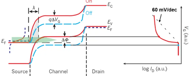
Therefore reduction of the static power consumption requires devices with a very steep subthreshold slope to minimize the off-current. Unfortunately, even the most innovative solutions in CMOS technology, such as FinFETs [3] or FDSOI [4] (Fully Depleted Silicon On Insulator) architectures, are unable to solve this problematic. The physics involved on the carrier injection mechanism of MOSFETs, thermionic emission of carrier overcoming a potential barrier, inherently tie the minimum achievable subthreshold swing value to 60 mV/dec at room temperature (Figure 2). This confirms the necessity to implement new physics in transistors in order to achieve very steep subthreshold slopes enabling the possibility to fabricate devices for ultra-low power applications (VDD < 0.4 V).
Figure 2. Subthreshold swing (SS) characterized in different CMOS technology generations. Last generation of planar structures SS was constrained to values close to 100 mV/dec. Only trigate architectures (FinFET or FDSOI) achieve SS values close to the thermal limit of 60 mV/dec [2].
The International Roadmap for Devices and Systems (IRDS) have identified a great number of devices with the potential capabilities to achieve SS below 60 mV/dec, called “Beyond-CMOS” devices [5]. However, there are important conditions to fulfill: firstly, the process fabrication of these steep slope devices must be compatible with the co-integration of MOSFETs. Secondly, the viability as a technology with possibilities to be extended for 3D Power scaling [6]. These conditions severely restrict the candidates, but Tunnel FETs (TFETs) still stand out as one of the most important. During the last decade TFETs have been extensively studied and considered as one of the most promising devices for ultra-low power applications. Unfortunately, the mismatch showed between experiments and simulations linked to the inability for achieving simultaneously a high on-current and a steep slope [7], focused the attention on other type of devices. Despite this context, TFET investigations are still ongoing because the technology is based on the same architecture, materials and boosters used in CMOS devices. This implies that successive improvements in process fabrication, specifically in junction formation and new epitaxy techniques for extremely thin film layers with a good quality control, will reveal the true performance of TFETs, that it is currently degraded.
The work of this thesis is focused on the study of FDSOI Tunnel FET devices from planar to trigate/nanowire structures. Its aim is to shed light on the capabilities of silicon or SiGe TFETs for ultra-low power applications. It also aims at identifying which are the major challenges that prevent TFETs to be co-integrated with CMOS technology. We have studied well-known parameters such as I-V characteristic, ION/IOFF ratio and subthreshold swing
which serve as performance indicators. We have measured devices made using different thermal budgets and extracted information on defects through charge pumping method and with low-frequency noise analysis (LFN). Using these measurements it is possible to differentiate whether TFET performance limitations are intrinsic to device physics or are a fabrication maturity issue. TCAD simulations were also used to evaluate possible device architecture improvements that can simultaneously lower the subthreshold slope and achieve higher high on-current.
The originality of this thesis work resides in:
1. The first demonstration of functional “Low-Temperature” (LT) Tunnel FETs based on a compatible CMOS process fabrication and with similar performance to conventional TFETs. This opens the door of TFETs as a potential candidate for 3D integration.
2. The confirmation that interface oxide traps and junction defects are not passivated enough with the LT annealing process. This results in a trap-assisted tunneling (TAT) effect, which generates a higher on-current in the subthreshold region that degrades the subthreshold slope.
3. The design and simulation of TFET device engineering and innovative planar architectures, proving the possibility to obtain simultaneously steep slope and high on-current via interband tunneling in extremely thin silicon films.
The manuscript is organized as follows:
Chapter 1. We explain why the equivalent scaling cannot overcome limitations on power
consumption and delay degradation in ICs. It is also noticed the importance of power efficiency in the emerging and profitable handheld device market and the limitations of MOSFET physics for low-voltage application. Lastly, we identified the most studied Beyond-CMOS devices and explained why Tunnel FETs are still one of the most promising steep slope devices in spite of the current challenges in device performance.
Chapter 2. It is dedicated to the operation principle of Tunnel FETs and, in particular,
the potential for achieving a steep subthreshold slope. Also, the main reasons for the discrepancy between simulated and fabricated devices are discussed. In addition, a TCAD study identifies the impact of different parameters (TSi, LG, LIN, EOT and materials) on
performance and allows one to highlight the most important challenges for TFET optimization. The structure and fabrication process of the TFETs made by the CEA are detailed and a list of the most interesting current research efforts on TFETs is provided. Finally, we benchmark the performance of the most important TFETs fabricated during the last decade.
Chapter 3. We report for the first time functional TFETs made with a low-temperature
process, indicating that can be a promising candidate for 3D Power scaling such as CoolCubeTM. Using an electrical characterization method called “Dual IDVD” it is possible to
determine if a device has a real interband tunneling behavior or if it is a Schottky FET. LT TFETs exhibit higher on-current and degraded off-current than their “High-Temperature” (HT) TFETs counterparts. Besides, a simulation study confirms the results obtained from experiments for gate overdrive voltages. Several hypotheses are made to explain this unexpected behavior.
Chapter 4. This chapter is focused on explaining why LT TFETs present a higher
on-current and a higher leakage on-current than HT devices. Charge pumping measurements confirm a higher density of interface states at the top interface in LT than HT TFETs. Besides, a low-frequency noise analysis confirms that LT devices exhibit more traps in the junctions that give place to TAT tunneling current instead of interband tunneling, which degrades the subthreshold slope. These results suggest the evidence that the main constraints for a good TFET operation are related with the maturity of the current process fabrication.
Chapter 5. This chapter is dedicated to an extensively TCAD simulation analysis of
innovative planar architectures to achieve simultaneously a steep subthreshold slope and a significant on-current. Best options rely on increasing the surface for the interband tunneling via extension of the tunneling junction into the body region. Also, a better electrostatic control can be achieved with extremely thin films.
Bibliography
[1] G. E. Moore, “Cramming More Components Onto Integrated Circuits,” Proc. IEEE, vol. 86, no. 1, pp. 82– 85, Jan. 1998.
[2] L. Zhang, J. Huang, and M. Chan, “Steep Slope Devices and TFETs,” in Tunneling Field Effect Transistor
technology, Springer, 2016, pp. 1–31.
[3] C.- Jan et al., “A 22nm SoC platform technology featuring 3-D tri-gate and high-k/metal gate, optimized for ultra low power, high performance and high density SoC applications,” in 2012 International Electron
Devices Meeting, 2012, pp. 3.1.1–3.1.4.
[4] C. Fenouillet-Beranger et al., “Low power UTBOX and back plane (BP) FDSOI technology for 32nm node and below,” in 2011 IEEE International Conference on IC Design Technology, 2011, pp. 1–4.
[5] A. Seabaugh et al., “Steep slope transistors: Tunnel FETs and beyond,” in 2016 46th European Solid-State
Device Research Conference (ESSDERC), 2016, pp. 349–351.
[6] M. Vinet et al., “Opportunities brought by sequential 3D CoolCubeTM integration,” in 2016 46th European
Solid-State Device Research Conference (ESSDERC), 2016, pp. 226–229.
[7] H. Lu and A. Seabaugh, “Tunnel Field-Effect Transistors: State-of-the-Art,” IEEE J. Electron Devices Soc., vol. 2, no. 4, pp. 44–49, Jul. 2014.
Context of the thesis and Beyond-CMOS devices
1.1. The end of planar scaling
Among all the available mechanisms to accomplish Moore’s trend [1] in a cost-effective way, miniaturization or geometry scaling was identified as one of the most important. In order to fulfill this requirement during 1980’s and 90’s the industry relied on the “constant-field scaling” method proposed by Dennard et al. [2], that considers the impact of the device geometry scaling on the device performance. Basically, reducing the size of transistors increases their density on a chip, which for a constant chip size, increases the functionality of the circuits for a lower cost. Unfortunately, in the new millennium pure geometrical scaling came to an end (and with that Dennard’s rules), because it was no longer possible to guarantee good electrostatic control of transistors due mainly to of Short-Channel Effects degrading the performance [3]:
1) Electric field-induced mobility degradation: the mobility of the carriers in the channel decreases when gate voltage is increased, due to surface roughness scattering.
2) Depletion capacitance of poly-Si gate and inversion layer capacitance: Both these effects increase the effective gate oxide thickness and, therefore, reduce the current drive of the transistor.
3) Subthreshold swing: the transistor cannot "instantly” switch from OFF to ON. The laws of thermodynamics impose the gate voltage to increase by at least
ln(10)×kT/q (= 60 mV) in order for the current below threshold to increase a tenfold.
4) Parasitic resistance of devices: the shorter the channel, the larger the relative importance of source, drain and contact resistances.
5) Leakage current (gate insulator leakage, gate-induced drain leakage).
6) Threshold voltage roll-off with gate length.
7) Drain-induced barrier lowering: threshold voltage decreases with drain voltage. In order to overcome all these undesired physical effects it is necessary to increase the performance via innovative boosters. Mobility degradation can be improved using different materials such as Germanium (with higher electron and hole mobility than silicon), SiGe or III-V compounds. Strain technology has also been widely used to boost mobility. Gate capacitance can be increased using high-k dielectrics in order to obtain a small EOT with a
relatively large dielectric film thickness, thereby avoiding gate tunnel current. Parasitic source and drain resistance is highly improved with raised source and drain and silicidation process. With respect to the off-current, the implementation of Silicon On Insulator (SOI) layers, isolating the body region from the substrate has demonstrated the reduction of leakage current by several orders of magnitude compared to bulk transistors. However, the issue of a steep subthreshold slope is still under investigation, CMOS technology is unable to provide a sub-thermal subthreshold slope (further explained in next section).
The implementation of these boosters is expensive and has caused a rapid increase of technology cost ($/mm2) in every new technological node below 130 nm. But according to recent data (Figure 1.1), this higher cost can be offset by higher transistor density per mm2 and by an increase of wafer volume production [4].
Figure 1.1. Increase of the cost/area in new nodes because of boosters and reduction of area/transistor with node scaling. Result is a reduction of the cost/transistor [4].
Moore’s law has continued the historical trend of increasing transistor count (More Moore), but in in the last decade new options such as co-integration of CMOS with other functions (More than Moore) have emerged. Silicon transistor scaling continues to deliver higher performance and lower power in a cost-effective way. There is a strong demand for further scaling due to a great number of services that request superior performance. For example data centers, based on clusters of servers and memory banks, have a power consumption into the hundreds of megawatts range [5]. Unfortunately, IRDS has foreseen that after 2027 there will be no room for further 2D geometrical scaling, because it is projected that the physical channel length of transistors would saturate around 12 nm. In addition, below 5-10 nm of gate length undesired direct source-to-drain tunneling takes place, increasing the leakage current and degrading the performance of the device.
Trigate architectures such as FinFETs offer better electrostatic control than planar MOSFETs and will be used as the key device architecture in order to extend 2D scaling until 2021 for high-performance logic applications. However, beyond 2019, scaling of passive elements such as interconnects becomes one of the major concerns as a consequence of tightening design rules. Even before reaching such small gate length, the delay of metal interconnections is already much larger than gate delay, hence the global delay of the integrated circuit is degraded due to the dominance of the capacitance of the metal lines (Figure 1.2).
Figure 1.2. Projection of on-chip electrical interconnect delays with technology scaling [6].
When this happens, it will be necessary to develop a new technology called monolithic 3D integration. The idea is to fabricate devices on top of each other to maintain the transistor density, but shortening the overall metal interconnection length. Currently under research on trigate architectures, a transition to Gate-All-Around (GAA) it is mandatory in order to reduce the power supply and keep a good electrostatic control. Eventually an evolution to vertical structures will be necessary: beyond-CMOS devices with steep slope and the addition of new functionalities, such as the integration of several memory circuits on top of logic circuits.
The integrated circuit is the concept that triggered the era of information and technology in which we are living nowadays and caused an inflection point in our society. In addition, it has transformed the semiconductor industry in a profitable market size of over $350 billion.
1.2. Towards the path of enhanced power efficiency
The first computer system developed by IBM (System/360) was fabricated based on bipolar solid logic technology. At that time, bipolar transistors were better switches and more reliable than any MOSFET device fabricated so far. On the contrary, they presented a higher cost and also a higher power consumption than MOSFETs. Despite these drawbacks, since only large corporations could afford to buy a computer, expensive heat dissipation systems were implemented in order to obtain the maximum performance. The computer industry relied on bipolar technology until early-1980’s. The apparition of the personal computer (1981) and the introduction of small computers at all levels of society confirmed that it was necessary to find an alternative to bipolar transistors, partly because large energy consumption was no longer sustainable. Therefore, CMOS technology with acceptable power consumption and lower cost than bipolar ICs, became the choice for logic and memory applications.
Figure 1.3. Power consumption of Intel’s CPUs in history. In early 2000’s the limit of 100 Watts was already reached [7].
Due to a lower switching energy in successive technology generations, each new released microprocessor could operate at higher frequencies and therefore, offered higher computer performance. Unfortunately, device shrinking was accompanied by an increase in IC power density. Figure 1.3 shows that the power consumption has increased from almost 2 W/cm2 in the i386 processor (1.5 µm gate length) to nearly 100 W/cm2 in Pentium processors (0.13 µm gate length). At this point it became clear that it would be impossible to simultaneously increase the transistor density and the operation frequency of microprocessors. Finally, the solution adopted was to continue increasing the number of transistors according to Moore’s law, while limiting the microprocessors operating frequency to a few GHz in order to make ICs able to work under practical thermal conditions. However, to solve the limitations of this constraint with respect to the output performance, it was necessary to modify the process architecture from single core to multi-core. With this approach, each core would run up to 2 GHz, while the total output rate of the microprocessor is fold by the output combination of the multiple cores.
In order to fabricate low power logic devices it is necessary to understand what is causing an increase of the energy consumption during the binary switching in a CMOS inverter:
(1.1)
Before specific ICs were fabricated for mobile phones, the voltage supply was still high (~3 V). From equation (1.1), one can notice that the most effective technique for decreasing power consumption in an integrated circuit is simply to reduce the supply voltage VDD.
However, Figure 1.4 shows that the scaling of VDD below 0.8 V has become extremely
challenging [8]. In order to keep up performance, which is proportional to the current drive
ID~(VDD– VTH)2, threshold voltage (VTH) must be decreased together with VDD. Reducing VTH
increases leakage current due to the finite value of the subthreshold slope, short channel effects and other effects such as random dopant fluctuation. This implies that for new technological nodes, the switching energy (~CVDD2) cannot be scaled as low as it should be
due to the unmatched VDD scaling and to the increase of short-channel effects with gate length
reduction. When the threshold voltage is lowered, the OFF current increases exponentially, such that the static power consumption (IOFF×VDD) reaches levels equal to those of the
Figure 1.4. Supply voltage scaling (VDD) based on Dennard’s rules (early 2000’s) and new material scaling
(up to 2010). Currently VDD scaling saturates at around 0.8 V [8].
1.2.1. CMOS limitation for low-voltage applications
Transport in MOSFET devices is based on the drift-diffusion mechanisms. For an N-type bulk MOSFET (p-type substrate) with no applied bias, majority carriers from source and drain junctions (electrons) diffuse into the channel region (Figure 1.5a). The same occurs for the majority carriers in the channel (holes) that diffuse towards the source and drain. As a result depletion regions are created in the junctions, together with potential barriers (local potential variations). Under thermodynamical equilibrium the diffusion current is exactly compensated by the drift current due to the potential variations. If a positive gate voltage is applied, the energy of the barriers start to decrease, electrons can diffuse from the source and drain in the P-type region, and an inversion layer is created at the channel surface, connecting the source and drain. If a positive drain voltage is applied, electrons can flow from source to drain.
Figure 1.5. (a) N-channel MOSFET device structure schematic; (b) Energy band diagram in flat-band zero-bias equilibrium condition. High energy barriers at the junctions prevent that electrons cross towards the drain terminal [9].
The channel charge density in a MOSFET is given by the Boltzmann distribution:
(1.2)
where s is the surface potential at the Si/insulator interface. As the subthreshold current is
proportional to the charge density, the drain current in a MOSFET can be expressed by [10]:
From equation (1.3) we can calculate the subthreshold swing, which is an important figure of merit to determine if a device is a good candidate for ultra-low power applications.
(1.4)
Subthreshold swing indicates how much voltage one must apply to the front gate terminal to achieve an increase change of the drain current by one order of magnitude. This provides a measure of how abruptly a device can be switched from off-state to on-state. A lower SS is desirable because it represents a sharper switching between the ON and OFF states. Conversely a higher SS implies "spending" a grand deal of gate voltage to turn the device from OFF to ON. The term m in equation (1.4) is the body factor and for a bulk MOSFETs is given by relationship m = 1+CD/Cox, where CD is the bulk depletion capacitance and Cox is the
gate oxide capacitance. Both Cox and CD are positive in CMOS technology, so the best case
scenario occurs when Cox>> CD and thus, m is close to unity although slightly greater. The
term n is given by:
(1.5)
Equation (1.5) confirms that the kT/q term is limiting the minimum achievable subthreshold slope of MOSFETs to 60 mV/dec at room temperature (300K). It is a fundamental limit due to the Boltzmann distribution of electrons in the energy bands. When SCEs began to degrade the electrostatic behavior of the devices (technology node 0.35 µm), the doping of the channel region was progressively increased to achieve reduced short-channel effects. However, a higher doping caused a reduction of the depletion width and therefore a higher CD (~ εsi/xdepl), increasing the body factor and the subthreshold swing. The
last bulk technology nodes based on planar architectures (from 90 nm to 32 nm) introduced high-k materials for the gate oxide to keep a constant CD/Cox ratio from node to node,
obtaining values of SS around 96 mV/dec [11]. However, this value is too high for low-power applications purposes. The introduction of trigate architectures such as FinFETs allows one to reduce the SCEs without increasing the channel doping and CD is significantly reduced (with
values of n close to 1.1), achieving SS values in the range of 65-75 mV/dec. Similar results are obtained for FDSOI architectures owing to the presence of the Buried Oxide (BOX) layer.
Figure 1.6. Transfer characteristic of a MOSFET showing that for a fixed subthreshold slope, reducing the threshold voltage implies a significant degradation (increase) of the off-current [12].
Unfortunately, it is not possible to reduce SS below 60 mV/dec in a MOSFET, even in the absence of SCEs.
Figure 1.6 shows that a reduction of the bias supply VDD requires also the proportional
reduction of VTH to maintain constant performance (constant current drive). However,
reducing VTH implies increasing the off-current and, therefore, increasing the static power
consumption. As a result, MOSFET technology is not suitable for ultra-low power applications (VDD < 0.4 V). The only way VTH can be reduced without increasing the OFF
current is to reduce the subthreshold slope (SS < 60 mV/dec). Such devices will need to be based on different physics principles with a different carrier injection mechanism than in MOSFET. An ideal steep slope switch enables the reduction of the threshold voltage without increasing the off-current (Figure 1.7) compared to a regular switch. There are two possibilities: either obtain a body factor slightly higher than unity (m > 1) and n < 60 mV/dec (Tunnel FETs, Phase-FETs) or m < 1 (negative capacitance effect) and n ~ 60 mV/dec as happens in Ferroelectric-gate "negative capacitance" FETs.
Figure 1.7. ID(VG) curves of a general switch and a steep slope switch. With a steep subthreshold slope it is
possible to reduce VTH without degrading the off-current [11].
1.3. Beyond-CMOS devices
Innovative computing paradigms and applications such as big data, artificial intelligence, exascale supercomputing and robotics are requesting simultaneously higher performance and efficiency requirements that are extremely challenging to provide using the current CMOS technology, despite of all the implemented boosters [13]. However, beyond-CMOS technologies based on state-of-the-art architectures, processes and materials open the door to new solutions that can be extended even for 3D power scaling. According to the European NEREID project, a significant investment effort has been done in emerging computing paradigms, namely: Quantum computing, Molecular Electronics, Spintronics, 2D materials, Neuromorphic computing and beyond-CMOS. Of course, the disruption from the classical von Neumann approach differs in each case. Quantum and Neuromorphic computing completely disrupts all system levels from device to algorithm [14], while for extended and beyond-CMOS only the device and logic levels are affected right now, although 3D power scaling will most likely also have an important impact on the processor’s microarchitecture.
Figure 1.8. Classification of beyond-CMOS devices based on the structure/materials (conventional or novel) and the computational variables charge (voltage, current), non-charge (spintronic, orbitronic) [13].
Figure 1.8 shows the classification done by IRDS for emerging logic devices, based on the level of innovation of structure/materials (similarity with the current CMOS process fabrication), with charge based devices (transistor-like) or non-charge devices (sprintronic or orbitronic). Recently, benchmarking studies have been published with beyond-CMOS devices for logic integrated circuits [15] and boolean and Neuromorphic representative circuits [16]. Despite the fact that the majority of devices are evaluated via simulations, results suggest a general trend indicating that steep slope switches present some advantages over high-performance CMOS in terms of lower switching energy, though they are inferior to CMOS in delay (slower switch). Now, we present some of the most promising steeper slope devices that have already been fabricated.
1.3.1. Impact ionization MOSFET (IMOS)
The impact-ionization field-effect transistor (IMOS) [17] uses modulation of the impact ionization (avalanche breakdown) of a gated p-i-n structure to realize sharp switching. Figure 1.9a shows the schematics of an n-channel IMOS device with an intrinsic region between gate and source. On the contrary to MOSFETs, where the carriers are supplied by thermal injection from the source to the channel, carriers in IMOS are provided by avalanche breakdown in the intrinsic region (LI) from the source to the channel when VG > VTH (Figure 1.9c). The role of
the gate is to accumulate electrons (N+ electrostatic doping) that reduce the effective length from the nominal value (OFF state) to that of the intrinsic region (ON state) increasing the lateral effective field.
Very steep slopes have been obtained for p-channel SOI IMOS (LG = 2 µm, LIN = 0.2 µm)
in the range of 10-15 mV/dec [18] and for complementary IMOS on SOI (LG = 200 nm = LIN)
down to 2 mV/dec with on-current similar to CMOS [19]. Unfortunately, the threshold voltage and the drain polarizations required to trigger avalanche breakdown are too large ( ~ 20 V), although the breakdown voltages scale down in smaller geometry devices with a reduced intrinsic region [18]. In addition, when the device is under stress with repeated measurements, the threshold voltage increases monotonically and the subthreshold swing is severely degraded. This is consequence of the high electric field needed for avalanche
breakdown, causing hot carrier injection into the gate dielectric. There are reliability issues because of damage created by the impact ionization process to the gate oxide and spacers.
Figure 1.9. (a) Schematics of an n-channel IMOS device. (b) Energy band diagram in off-state. When VG <
VTH the electric field between channel and drain is not high enough to trigger the impact ionization. (c)
For VG > VTH, the effective channel length is reduced and avalanche breakdown is triggered, causing an
abrupt increase of the drain current [20].
1.3.2. Z
2-FET
The Z2-FET is a forward biased p-i-n diode fabricated in FDSOI technology and featuring an intrinsic region (LIN), which is not covered by the front gate. Figure 1.10a presents the
schematics of a p-type Z2-FET, where the P+ source is grounded (VS= 0), and the N+ drain is
forward biased (VD < 0). The negative and positive polarizations of the front and bottom gates
(VG < 0, VBG > 0) create a hole injection barrier in the LG region and an electron injection
barrier in LIN region, disabling the carrier flow at low drain voltage. With this configuration
we have a pnpn thyristor-like structure. The operation principle of the Z2-FET involves a strong positive feedback between the carrier flow and the gate-controlled injection barriers that turns on the device sharply due to the suppression of both injection barriers (with no need of impact ionization) [21]. The ID(VG) curve in Figure 1.10b shows an abrupt subthreshold
slope (< 1 mV/dec), a high current ION/IOFF ratio > 10
8
at supply voltage around 1 V.
Figure 1.10. (a) Schematic of a p-type Z2-FET. (b) Transfer characteristics showing a steep subthreshold slope for a Z2-TFET with TSi = 20 nm, TBOX = 145 nm, LG = 400 nm and LIN = 500 nm [22].
The ID(VD) curves of the Z2-FET exhibit a gate-controlled hysteresis, which in fact limits
the possibilities of this steep switch device for logic circuits unless very fast pulses are applied on the gate [23]. On the other hand, the hysteresis makes the Z2-FET very interesting for memory applications, such as capacitor-less transistor DRAM (1T-DRAM), single-transistor SRAM or Electrostatic Discharge (ESD) protection and charge sensors.
1.3.3. Negative capacitance FET (NC-FET)
The negative capacitance MOSFET aims at achieving a steep slope by boosting the increase of the surface potential φs with respect to the gate voltage, instead of modifying the
carrier injection mechanism. In conventional MOSFETs fabricated with high-k dielectrics, Cox
is always positive and it is not possible to achieve a body factor m < 1. To reduce the body factor below unity, one can replace part of the gate dielectric by a material that has a "negative capacitance", which can be obtained using some ferroelectric materials [24]. Using such a gate stack, the surface potential can increase faster than the gate voltage, creating a large amount of charge and a higher current compared to a conventional MOSFET. Experimental devices with ferroelectric/SiO2 gate stack reporting a SS of 13 mV/dec have
been demonstrated [25]. Unfortunately, a permanent polarization of the ferroelectric layer is usually observed, which results in a shift of the threshold voltage and a hysteresis effect in the
ID(VG) curves. This effect is extremely useful for memory applications but it jeopardizes the
use of such materials for logic gates, because the gate voltage partly loses ability to turn off the device. Different solutions to suppress the hysteresis can be found in the literature.
Figure 1.11. ID(VG) curves of a Fe-HZO FET showing a reduced hysteresis window of 0.1 V and a
subthreshold swing below 60 mV/dec for forward and reverse bias ramps [26].
Recently, a ferroelectric HfZrOx (Fe-HZO) FET was reported exhibiting a small hysteresis window with a VT shift below 0.1 V (Figure 1.11) and a subthreshold swing below
60 mV/dec [26]. Moreover, some strategies to achieve hysteresis-free devices have been proposed, for example a gate stack formation of Fe-HZO/epi-Ge/Si FETs with an experimental 3 mV VTH shift [26] and the first reported NC-FinFET with HfZrO2 with higher
ferroelectricity (higher crystallinity by annealing at higher temperature) that suppresses the hysteresis [27]. Despite of all the efforts, there are still important challenges with respect to the ferroelectric material growth and process compatibility with conventional MOSFET process fabrication.
1.3.4. Nano-electromechanical Switches (NEMS)
Nano-electromechanical switches (NEMS) based on a mobile gate have also been considered for ultra-low power applications, because of two important characteristics: firstly, they feature a zero off-state leakage current and secondly, they have a zero subthreshold swing [28]. In early 2000’s a device called the NEM-FET was proposed, which combined a conventional MOS transistor and a suspended metal membrane [29], [30] as shown in Figure 1.12a. The operation principle is simple: when a gate voltage is applied, there is an electric field-induced force (felec) that reduces the air gap, so the intrinsic voltage in the gate oxide is
tuned with the capacitor divider formed by Cair and Cox.
Figure 1.12. (a) Schematic of a Suspended-Gate MOSFET with a mobile gate terminal [30]. (b) Schematic of a planar three terminal electrostatic switch [31].
Simultaneously, an elastic force appears (felas) with same magnitude as felec, but in
opposite direction. At a given gate voltage Vpi (pull-in voltage) the system balance is lost and
the gate terminal connects to the gate oxide. Therefore, there is abrupt change in the surface potential (amplification) from the intrinsic voltage to the Vpi, which induces an increase of the
drain current. An experimental SS of 2 mV/dec was reported, together with an ultra-low leakage current (< 0.1 pA) due to the air gap [30]. However, the gate voltage required to trigger the effect is quite high (~9 V). Furthermore, a shift in the Vpi voltage appears after
several OFF/ON cycles due to oxide degradation, giving rise to a hysteresis effect. This renders the device rather unsuitable for logic applications. In addition, this device cannot be easily scaled down.
During last decade, a great effort has been done to improve the design (Figure 1.12b) and reliability of integrated circuits based on mechanical relays [31], but miniaturization is still one of the main challenges. Unfortunately, logic NEMS still suffers from requiring large supply voltages and large area compared to MOSFETs. In addition, the fabrication steps are very different from those used in conventional CMOS technology [28]. Nowadays, the use of electromechanical switches is oriented to auxiliary devices to help conventional CMOS circuits for being more energy efficient, for example as non-volatile elements to facilitate the power gating without data loss in the registers. The idea is to use the back-end-of-line process to integrate 3D NEMS switches with CMOS transistors for ultra-low power logic and memory circuits.
1.3.5. Tunnel FETs (TFETs)
Tunnel FETs are considered as one of the most feasible contenders for ultra-low power applications because they have the theoretical capability of providing a sub-thermal subthreshold slope. This is possible because TFETs rely on interband tunneling as carrier injection mechanism, which is temperature independent. Unfortunately, TFETs are very sensitive to defects located in the semiconductor region and at the interface. The trap-assisted tunneling (TAT) mechanism, which is temperature dependent, is causing band-to-band tunneling (BTBT) to occur when the device is supposed to be turned off, resulting in a generation current that degrades the subthreshold slope. This explains why very few experimental TFETs reach a SS below 60 mV/dec [32].
A qualitative comparison between TFETs and the rest of the previously listed steep-slope devices suggests that TFETs have a lower on-current and a less steep subthreshold slope than the IMOS, the Z2-FET, the NC-FET and NEMS. However, the TFET is still the most studied and fabricated steep-slope switch device for low-power logic applications purposes. The main reason for so much research ongoing on TFETs is that TFETs have the same architecture/materials boosters as CMOS devices, and thus their fabrication is compatible with CMOS. In addition, TFETs do not present hysteresis effects and the gate terminal has full control on the device operation. According to the IRDS, the TFET is one on the most viable devices for the 3D power scaling and can be co-integrated with CMOS for future applications leveraging many parallel cores.
For these reasons, it is so important to understand the major problems that prevent TFETs from simultaneously achieving a steep slope and a high on-current, and to explore solutions that can eventually solve these issues.
1.4. Conclusions
Silicon transistor scaling continues to deliver higher performance and lower power in a cost-effective way for each new technology generation. In order to accomplish the control of the SCEs, the equivalent scaling allows one to increase the performance not only through geometry reduction, but also via innovative materials and new architectures based on multiple gates such as FinFET or FDSOI technology to enhance the effective electrostatic control.
State-of-the-art microprocessors are nowadays designed based on very tight and restrictive power consumption rules. Currently, deliver the highest performance possible is no longer always the major concern; we need to provide the maximum performance at the lowest possible power consumption. Unfortunately, equivalent scaling cannot overcome the limitations on power consumption and delay degradation in logic integrated circuits. Moreover, specific integrated circuits for ultra-low power applications will demand a bias supply lower than 0.4 V, but in CMOS technology scale VDD below 0.8 V has become
extremely challenging. The reason is that the physics involved on the carrier injection mechanism of MOSFETs, limits the subthreshold swing to a minimum value of 60 mV/dec at room temperature. VDD reduction requires also the proportional reduction of the threshold
voltage to maintain a constant performance. However, VTH reduction increases the off-current
and therefore the static power consumption. As a result, MOSFET technology is not suitable for ultra-low power applications (VDD < 0.4 V). It is mandatory to introduce new physics in
the transistors to modify the carrier injection mechanism.
Beyond-CMOS devices have the capabilities to achieve a sub-thermal subthreshold slope (SS < 60 mV/dec). IRDS have identified a great number of potential candidates, but here we highlight the most feasible candidates besides from Tunnel FETs, namely: Impact ionization MOSFET (IMOS), Z2-FET, Negative capacitance FET (NC-FET) and Nano-electromechanical Switches (NEMS). Despite of the general low performance of TFETs architectures, this technology is still considered the most promising contender for ultra-low power applications since it fulfills important conditions: firstly, TFET process fabrication is fully compatible with the co-integration with MOSFETs. Next, TFETs do not present hysteresis effect that degrades the electrostatic control for logic purposes. Finally, IRDS has identified TFETs as a viable technology with significant capabilities to be extended for 3D Power scaling.
The key messages of this chapter are: First, in next decade the semiconductor industry
will face the end of 2D geometrical equivalent scaling, and new options as co-integration of
CMOS with other functions will emerge. Secondly, tightening integrated circuits design
requirements for ultra-low power consumption (bias supply) are unattainable for MOSFET technology and new physics in transistors are necessary. Beyond-CMOS
devices have the potential capabilities to provide sub-thermal subthreshold slopes. Specifically, Tunnel FET technology gathers the most important conditions to be
considered a realistic choice for 3D Power scaling. This thesis aims at determining the nature of the TFET performance limitations and the possible solutions.
![Figure 1.2. Projection of on-chip electrical interconnect delays with technology scaling [6]](https://thumb-eu.123doks.com/thumbv2/123doknet/12731580.357293/26.892.180.695.111.466/figure-projection-chip-electrical-interconnect-delays-technology-scaling.webp)
![Figure 1.3. Power consumption of Intel’s CPUs in history. In early 2000’s the limit of 100 Watts was already reached [7]](https://thumb-eu.123doks.com/thumbv2/123doknet/12731580.357293/27.892.226.659.107.387/figure-power-consumption-intel-cpus-history-watts-reached.webp)
![Figure 1.8. Classification of beyond-CMOS devices based on the structure/materials (conventional or novel) and the computational variables charge (voltage, current), non-charge (spintronic, orbitronic) [13]](https://thumb-eu.123doks.com/thumbv2/123doknet/12731580.357293/31.892.232.644.114.385/classification-structure-materials-conventional-computational-variables-spintronic-orbitronic.webp)
![Figure 2.2. Energy band diagrams of a tunnel diode in forward bias; (a) at zero bias; (b) peak tunneling current; (c) valley current; (d) diffusion current [4]](https://thumb-eu.123doks.com/thumbv2/123doknet/12731580.357293/41.892.114.768.106.350/figure-energy-diagrams-forward-tunneling-current-current-diffusion.webp)

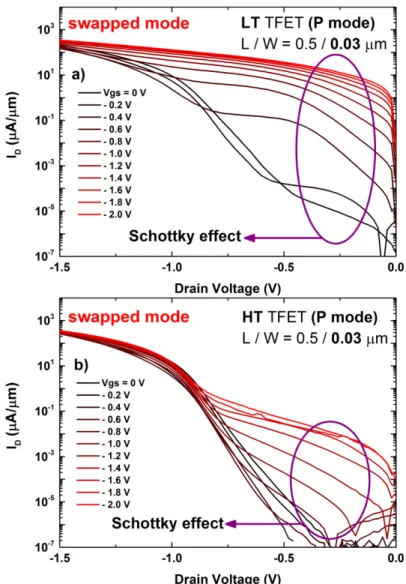
![Figure 3.5. Example of dual I D (V DS ) measurements of (a) LT TFET and (b) HT TFET, performed according to the TFET validation method detailed in [19] and showing that tunneling is BTBT and not Schottky related](https://thumb-eu.123doks.com/thumbv2/123doknet/12731580.357293/82.892.187.705.347.942/example-measurements-performed-according-validation-detailed-tunneling-schottky.webp)