A Diamond:H/WO3 Metal–Oxide–
Semiconductor Field-Effect Transistor
The MIT Faculty has made this article openly available. Please share
how this access benefits you. Your story matters.
Citation
Yin, Zongyou et al. "A Diamond:H/WO3 Metal–Oxide–Semiconductor
Field-Effect Transistor." IEEE Electron Device Letters 39, 4
(February 2018): 540 - 543 © 2018 IEEE
As Published
http://dx.doi.org/10.1109/led.2018.2808463
Publisher
Institute of Electrical and Electronics Engineers (IEEE)
Version
Author's final manuscript
Citable link
https://hdl.handle.net/1721.1/126179
Terms of Use
Creative Commons Attribution-Noncommercial-Share Alike
8 First Author et al.: Title
Abstract—A p-type Diamond:H/WO3 MOSFET based on surface
transfer doping is demonstrated. Using a low-temperature ALD-grown HfO2 as gate insulator, the Diamond:H/WO3 MOSFETs show excellent
output characteristics, gate-controllable 2-D hole gas and low gate leakage current. Long-channel FETs exhibit improved subthreshold behavior but reduced transconductance with respect to short-channel devices. An observed WO3-thickness dependent threshold voltage is
consistent with enhanced surface transfer doping as the WO3 layer is
thinned down. Low-temperature measurements suggest a significantly lower mobility than expected in this material system. This illustrates the challenge of maintaining high TMO quality during device fabrication.
Index Terms—Diamond:H, gate length, surface transfer
doping, temperature, WO3 thickness.
I. INTRODUCTION
Diamond is an ultra-stable material with a wide band gap of 5.47 eV. Recently developed surface transfer doping (STD) has opened a new avenue to exploit the excellent electrical and thermal properties of diamond [1]. The negative electron affinity that results after diamond surface hydrogenation (Diamond:H or, simply, D:H) enables the transfer of electrons from Diamond:H to high work-function acceptors located at its surface. This results in the formation of a two-dimensional hole gas (2DHG) at the Diamond:H surface.
Up to this date, water [2], fullerenes (C60) [3], fluorinated
Fullerenes (C60Fx, x = 18, 36, 48) [4], zinc-tetraphenylporphyrin
(ZnTPP) coupled C60F48 [5], Tetrafluoro-tetracyanoquinodimethane
(F4-TCNQ) [6], and more recently transition-metal oxides (TMOs)
[7]–[10], have been investigated as surface acceptors for D:H. Among these, TMOs such as MoO3, WO3, ReO3 and V2O5, stand out
with their unique properties of wide-band gap and high electron affinity. As a typical TMO, MoO3 was first used as acceptor on
Diamond:H and metal-oxide-semiconductor field-effect transistors (MOSFETs) have been demonstrated [11]. Separately, MoO3 has also
been used as a gate dielectric for Diamond:H MOSFETs [12]. D:H/V2O5 MISFETs have also been reported [13].
Manuscript received xxx; accepted xxx. Date of publication xxx; date of current version xxx. This work was supported by a Prof. Amar G. Bose Research Grant and in part by the US-Israel Bilateral Science Foundation (Grant #2014506). The review of this letter was arranged by Editor xxx.
Z. Yin# is with Research School of Chemistry, The Australian National
University, Canberra, ACT 2601 Australia (e-mail: [email protected]).
M. Tordjman# and R. Kalish are with the Solid State Institute,
Technion-Israel Institute of Technology, Haifa 32000, Israel (e-mail: [email protected]).
Z. Yin#, M. Tordjman#, A. Vardi and J. A. del Alamo are with
Microsystems Technology Laboratories, Massachusetts Institute of Technology, Cambridge, MA 02139 USA (e-mail: [email protected]).
# These authors contributed equally to this work.
Color versions of one or more of the figures in this letter are available online at http://ieeexplore.ieee.org. Digital Object Identifier xxx.
Most recently, D:H/WO3 has been found to have enhanced
charge-transfer robustness and efficiency [14], as compared to the D:H/MoO3 and D:H/V2O5 systems. A Hall-effect study of
thermally-evaporated WO3 on D:H measured a record areal hole
carrier concentration of 4.8×1014 cm-2 at a temperature up to 150oC
[14]. The hole mobility reached over 100 cm2V-1s-1 for temperatures
up to 300°C. In an effort to take advantage of the outstanding charge-transfer properties of this system, in this work we demonstrate the first implementation of a MOSFET in the D:H/WO3 system.
Moreover, we investigate the impact of WO3 thickness, gate length
and low temperature operation in the device characteristics.
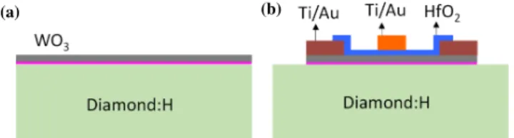
Fig. 1. Schematic cross-section of (a) starting heterostructure and (b) p-type Diamond:H/WO3 MOSFET.
II. DEVICE FABRICATION
Figure 1 shows a schematic cross section of the starting heterostructure and the fabricated MOSFET. Three 3×3×0.5 mm3 type IIa (001)-oriented single-crystal diamond substrates supplied from Element6, with nitrogen concentration < 1 ppm were used. Surface hydrogenation was performed by exposure to pure hydrogen plasma in a CVD reactor at 600°C for 40 minutes. Subsequently, the samples were heated at 350°C to desorb H2O
molecules and contaminants from the diamond surface in vacuum [11]. This was immediately followed by low-rate (0.1 Å/min) thermal evaporation of different thicknesses (2.4, 3.4 and 4.8 nm) of WO3 in
each sample. A surface roughness of Ra ~ 0.6 nm over an area of 1
µmx1 µm was measured by AFM, and a WO3 thickness uniformity of
10% was evaluated by ellipsometry. The stoichiometry and thickness of WO3 was characterized by X-ray photoelectron spectroscopy and
ellipsometry and results similar to those reported in Ref. 14 were obtained.
The process continues with electron-beam evaporation of Ti/Au (20/200 nm), as source and drain electrodes, through a shadow mask. Following this, 20 nm of HfO2 as gate dielectric layer was grown by
atomic layer deposition (ALD) at 150°C. The use of a gate oxide was deemed essential to obtain a working FET since WO3 is expected to
become highly conductive after the surface transfer process [14]. After that, flowable oxide (FOX) was spin coated on the sample surface and exposed by electron-beam lithography (EBL). This forms a hard mask that is used to define the active channel. Reactive-ion etching based on a BCl3/Cl/Ar chemistry was performed to etch the
exposed HfO2 and WO3 and to desorb the Hydrogen from the
diamond surface. FOX was then striped with a buffered oxide etchant. Subsequently, a standard photolithographic liftoff step was used to create a Ti/Au (10/100 nm) gate electrode at the center of the channel of the FETs. Devices with gate lengths (Lg) ranging from 0.7
to 5 µm and a constant gate width (Wg) of 20 µm were fabricated.
The source-drain distance gradually increased from 29 µm to 58 µm
A Diamond:H/WO
3Metal-Oxide-Semiconductor Field-Effect Transistor
Zongyou Yin
#, Moshe Tordjman
#, Alon Vardi, Rafi Kalish, and Jesús A. del Alamo, Fellow, IEEE
8 First Author et al.: Title
(a) (b)
(c)
as the gate length changed from 0.7 µm to 5 µm.
In this first demonstration, no effort was given to bringing the source and drain ohmic contacts directly onto the D:H surface. Rather, the goal of this work was to demonstrate the viability of the D:H/WO3 as a MOSFET system.
III. RESULTS
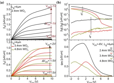
Fig. 2 shows electrical characteristics of typical MOSFETs with Lg
= 4 µm and different WO3 thickness. All devices show well saturated
drain current behavior with sharp pinchoff and low output conductance (Figs. 2a and 2b). The 2.4 nm WO3 MOSFETs show
greater drain current, Id, and transconductance, gm (Fig. 2b), and a
more positive threshold voltage, VT. These results are consistent with
recent Hall effect observations of decreased surface transfer efficiency and a reduced sheet hole concentration (from 2.5×1014 cm-2 to 1.3×1014 cm-2) of D:H with increasing WO
3 thicknesses (from
1.2 nm to 4.8 nm) [14].
The thinner WO3 devices also show greater gate leakage current,
Ig, (Fig. 2b). This also results in worse drain current saturation (Figs.
2a and 2b). A more effective electron transfer into the 2.4 nm thick WO3 layer is a plausible explanation for the larger gate current.
10-6 10-5 10-4 10-3 10-2 10-1 100 101 |Id |,|Ig | [ µ A/ µ m ] -2 0 2 4 6 8 0.0 0.2 0.4 0.6 VGS [V] gm [µ S/ µ m ] 3.4nm WO3 4.8nm WO3 2.4nm WO3 VDS=-6V, Lg=4µm 0.0 0.5 1.0 1.5 2.0 2.5 3.0 3.5 Lg=4µm |Id | [ µ A/ µ m ] 2.4nm WO3 VGS=-1V VGS=-1V VGS=9V 0 2 4 6 8 10 0.0 0.2 0.4 0.6 0.8 1.0 1.2 Lg=4µm 4.8nm WO3 3.4nm WO3 -VDS [V] |Id | [ µ A/ µ m ] VGS=-2V VGS=-1.5V VGS=11.5V Ig Id
Fig. 2. Output (a) and transfer (b) characteristics for Lg=4 µm
Diamond:H/WO3 FETs with WO3 thickness ranging from 2.4 nm to 4.8 nm.
Fig. 3. Subthreshold characteristics (a), gm characteristics (b) and ON
resistance (c) for 4.8 nm-thick WO3 Diamond:H/WO3 FETs with gate width
of 20 um and different gate lengths ranging from 0.7 µm to 5 µm.
We have studied the impact of gate length, Lg, on the electrical
characteristics of 4.8 nm-thick WO3 devices. This is graphed in Fig.
3. Fig. 3a shows that the subthreshold behavior rapidly improves as Lg increases. This probably stems from a combination of
short-channel effects and reduced Ig. In addition, we observe that the
peak transconductance, gm_max, for short Lg (≤1 µm) devices is about
3X that of long Lg (≥2 µm) devices (Fig. 3b). The threshold voltage,
VT, shifts positive as gate length shortens. This could be explained by
severe short-channel effects that arise from the use of a relatively thick gate dielectric coupled with the absence of body doping [15].
In addition, we extracted the ON resistance of 4.8 nm-thick WO3
transistors with different Lg at VGS=1 V and VDS=0.1 V (Fig. 3c).
From extrapolation of these data to Lg=0, we estimated a total
source/drain access resistance of ∼ 1700 kΩ•µm.
We have also studied the effect of temperature on the electrical characteristics of a Lg=5 µm, WO3=4.8 nmFET at 77 K. The results
are presented in Fig. 4. At 77 K, we observe a large increase in Id and
gm with gm_max scaling up by 3.5 times. We also see that Ig was
reduced by about two orders of magnitude (Fig. 4b). This results in significantly improved subthreshold behavior with the minimum subthreshold swing (Smin)scaling down from ∼ 1225 mV/dec to ∼ 190
mV/dec and the ON-OFF ratio improving from ∼ 103 to ∼ 106, as the
temperature is reduced from RT to 77K.
Fig. 4. Output (a) and transfer (b) characteristics for Lg=5 µm, WO3=4.8 nm
Diamond:H/WO3 FETs measured at 77 K and RT.
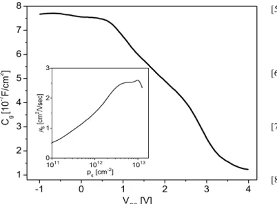
Device operation at 77 K was further studied by carrying out capacitance-voltage (Cg-VGS) and I-V transfer (Id-VGS) characteristics
in a device with 4.8 nm of WO3 and Lg=5 µm. The C-V
characteristics were measured at 1 MHz with VDS=0 V. Id-VGS
measurements were performed at VDS=-2 V. A typical Cg-VGS result
is shown in Fig. 5. From these data, we extract the gate voltage dependence of the sheet hole concentration (ps) and hole mobility
(µp) [16],[17]. For this, we used a dielectric constant of 13 for HfO2
(in consideration of the low ALD temperature of 150oC [18]) and 5
for WO3. Also, in order to correct for parasitic resistance, the
source/drain access resistance at 77 K, was estimated as Rsd_77K=∼
908 kΩ•µm from its RT value by using Rsd_RT=Rsd_77K ×
[1+α(TRT-T77K)], where α is the temperature coefficient of the
resistance. A value of α=0.004 was estimated from the slope (resistance of RRT and R77K) of the Id-VDS curve under VDS=0.1 V and
VGS=0 at RT for RRT and 77K for R77K, using an identical equation:
RRT=R77K × [1+α(TRT-T77K)].
The inset of Fig. 5 graphs the sheet hole mobility (µs) vs. sheet
hole concentration (ps). Over most of its range, the mobility increases
with hole concentration. This suggests that Coulomb scattering dominates at low temperature. We observe a maximum sheet hole concentration of about 1.3×1013 cm−2, an excellent value that shows
the promise of this material system for high current applications. The corresponding mobility, however, is 2.6 cm2/V·sec. This is much
(a) (b)
8 First Author et al.: Title
lower than results obtained from Hall measurements at room temperature of similar unprocessed samples [14]. This is also consistent with Coulomb scattering that could be due to gap states introduced as a result of WO3-x reduction during the device
fabrication process [19]. The reduction in resistance that is observed as the temperature drops could be due to a insulator-to-metal transport transition recently reported by Mattoni et al. in WO3-x [20].
This would also result in a reduced work function and degraded surface transfer doping efficiency at room temperature [19].
-1 0 1 2 3 4 1 2 3 4 5 6 7 8 VGS [V] Cg [10 -7 F/cm 2 ] 1011 1012 1013 0 1 2 3 µs [cm 2/Vs ec] ps [cm-2]
Fig. 5. Split C-V measurements at 1 MHz of a typical Diamond:H/WO3 FET
(Lg =5 µm, Wg=20 µm, WO3=4.8 nm) at 77 K. Inset: sheet hole mobility vs.
sheet hole concentration.
Our results reveal the potential of the D:H/WO3 system for future
transistor applications but also illustrate the challenge of maintaining high TMO quality during device fabrication, an issue already noted in [11]. To exploit the advantageous properties of the D:H/TMO system, transistor fabrication processes will need to be developed that maintain the integrity of the TMO layer.
IV. CONCLUSIONS
We demonstrate for the first time p-type Diamond:H/WO3 FETs.
Long-channel devices display well behaved transistor characteristics with 103 ON-OFF ratio at room temperature. An anomalous threshold voltage dependence on WO3 thickness is observed which is
consistent with enhanced surface transfer doping as the WO3 layer is
thinned down. Low-temperature mobility measurements suggest strong Coulomb scattering perhaps due to WO3 degradation during
the fabrication process. ACKNOWLEDGMENT
Device fabrication was carried out at the Microsystems Technology Laboratories and the Electron Beam Lithography Facility at MIT.
REFERENCES
[1] O. A. Williams and R. B. Jackman, “Surface conductivity on hydrogen terminated diamond,” Semicond. Sci. Technol., vol. 18, no. 3, pp. S34–S40, 2003. DOI: stacks.iop.org/SST/18/S34.
[2] F. Maier, M. Riedel, B. Mantel, J. Ristein, and L. Ley, “Origin of surface conductivity in diamond,” Phys. Rev.
Lett., vol. 85, no. 16, pp. 3472–3475, 2000. DOI:
https://doi.org/10.1103/PhysRevLett.85.3472.
[3] P. Strobel, J. Ristein, L. Ley, K. Seppelt, I. V. Goldt, and O. Boltalina, “Surface conductivity induced by fullerenes on diamond: Passivation and thermal stability,” Diam. Relat.
Mater., vol. 15, no. 4–8, pp. 720–724, 2006. DOI:
https://doi.org/10.1016/j.diamond.2005.10.034.
[4] M. T. Edmonds, M. Wanke, A. Tadich, H. M. Vulling, K. J. Rietwyk, P. L. Sharp, C. B. Stark, Y. Smets, A. Schenk, Q. H. Wu, L. Ley, and C. I. Pakes, “Surface transfer doping of hydrogen-terminated diamond by C 60F 48: Energy level scheme and doping efficiency,” J. Chem. Phys., vol. 136, no. 12, 2012. DOI: https://doi.org/10.1063/1.3695643
[5] D. P. Langley, Y. Smets, C. B. Stark, M. T. Edmonds, A. Tadich, K. J. Rietwyk, A. Schenk, M. Wanke, Q. H. Wu, P. J. Barnard, L. Ley, and C. I. Pakes, “Surface transfer doping of diamond with a molecular heterojunction,” Appl. Phys.
Lett., vol. 100, no. 3, pp. 032103, 2012. DOI:
https://doi.org/10.1063/1.3676445.
[6] D. Qi, W. Chen, X. Gao, L. Wang, S. Chen, P. L. Kian, and A. T. S. Wee, “Surface transfer doping of diamond (100) by tetrafluoro-tetracyanoquinodimethane,” J. Am. Chem. Soc., vol. 129, no. 26, pp. 8084–8085, 2007. DOI: 10.1021/ja072133r.
[7] S. A. O. Russell, L. Cao, D. Qi, A. Tallaire, K. G. Crawford, A. T. S. Wee, and D. A. J. Moran, “Surface transfer doping of diamond by MoO3: A combined spectroscopic and Hall
measurement study,” Appl. Phys. Lett., vol. 103, no. 20, pp. 202112, 2013. DOI: https://doi.org/10.1063/1.4832455. [8] M. Tordjman, C. Saguy, A. Bolker, and R. Kalish, “Superior
Surface Transfer Doping of Diamond with MoO3” Adv. Mater. Interfaces, vol. 1, no. 3, pp. 1–6, 2014.
DOI: 10.1002/admi.201300155.
[9] K. G. Crawford, L. Cao, D. Qi, A. Tallaire, E. Limiti, C. Verona, A. T. S. Wee, and D. A. J. Moran, “Enhanced surface transfer doping of diamond by V2O5 with improved
thermal stability,” Appl. Phys. Lett., vol. 108, no. 4, pp. 042103, 2016. DOI: https://doi.org/10.1063/1.4940749. [10] C. Verona, W. Ciccognani, S. Colangeli, E. Limiti, M.
Marinelli, and G. Verona-Rinati, “Comparative investigation of surface transfer doping of hydrogen terminated diamond by high electron affinity insulators,” J. Appl. Phys., vol. 120, no. 2, pp. 025104, 2016. DOI: https://doi.org/10.1063/1.4955469.
[11] A. Vardi, M. Tordjman, J. A. Alamo, and R. Kalish, “A Diamond : H/MoO3 MOSFET,” IEEE Electron Device Lett.,
vol. 35, no. 12, pp. 1320–1322, 2014. DOI: 10.1109/LED.2014.2364832.
[12] Z. Ren, J. Zhang, J. Zhang, C. Zhang, S. Xu, Y. Li, and Y. Hao, “Diamond Field Effect Transisotrs With MoO3 Gate
Dielectric,” IEEE Electron Device Lett., vol. 38, no. 6, pp. 786–789, 2017. DOI: 10.1109/LED.2017.2695495.
[13] C. Verona, W. Ciccognani, S. Colangeli, E. Limiti, M. Marinelli, G. Verona-Rinati, D. Cannatà, M. Benetti, and F. D. Pietrantonio, “V2O5 MISFETs on H-Terminated
Diamond,” IEEE Electron Device Lett., vol. 63, no. 12, pp. 4647–4653, 2016. DOI: 10.1109/TED.2016.2617362. [14] M. Tordjman, K. Weinfeld, and R. Kalish, “Boosting
Surface Charge-Transfer Doping Efficiency and Robustness of Diamond with WO 3 and ReO3,” Appl. Phys. Lett.,111,
pp. 111601, 2017. DOI: https://doi.org/10.1063/1.4986339. [15] J. A. del Alamo, Integrated Microelectronic Devices: Physics
and Modeling, 1st Edition, Pearson Publication., Sec 10.2, 2017.
[16] B. Radisavljevic, A. Radenovic, J. Brivio, V. Giacometti, and A. Kis, “Single-layer MoS2 transistors,” Nat.
Nanotechnol., vol. 6, no. 3, pp. 147–150, 2011. DOI:
[17] S. Balendhran, J. Deng, J. Z. Ou, S. Walia, J. Scott, J. Tang, K. L. Wang, M. R. Field, S. Russo, S. Zhuiykov, M. S. Strano, N. Medhekar, S. Sriram, and M. Bhaskaran, “Enhanced Charge Carrier Mobility in Two-Dimensional High Dielectric Molybdenum Oxide,” Adv. Mater., vol. 25, pp. 109–114, 2013. DOI: 10.1002/adma.201203346. [18] H. Jung, H. Jeon, K. Kim, I. Yu, Y. Lee, J. Lee, J. Chung, D.
Cho, N. Lee, J. Park, J. Choi, S. Han, and C. Seong, “The Impact of Carbon Concentration on the Crystalline Phase and Dielectric Constant of Atomic Layer Deposited HfO 2 Films on Ge Substrate,” ECS J. Solid State Sci. Technol., vol. 1, no. 2, pp. 33–37, 2012. DOI: 10.1149/2.020202jss. [19] M. Greiner, L. Chai, M. Helander, W. Tang, and Z. Lu,
“Transition Metal Oxide Work Functions: The Influence of Cation Oxidation State and Oxygen Vacancies,” Adv. Funct.
Mater., vol. 22, pp. 4557-4568, 2012. DOI: 10.1002/adfm.201200615.
[20] G.Mattoni, A. Filippetti, N. Manca, P. Zubko, and A. D. Caviglia, “Charge doping and large lattice expansion in oxygen-deficient heteroepitaxial WO3,”