HAL Id: hal-00446088
https://hal.archives-ouvertes.fr/hal-00446088
Submitted on 12 Jan 2010HAL is a multi-disciplinary open access archive for the deposit and dissemination of sci-entific research documents, whether they are pub-lished or not. The documents may come from teaching and research institutions in France or abroad, or from public or private research centers.
L’archive ouverte pluridisciplinaire HAL, est destinée au dépôt et à la diffusion de documents scientifiques de niveau recherche, publiés ou non, émanant des établissements d’enseignement et de recherche français ou étrangers, des laboratoires publics ou privés.
Compact and explicit physical model for lateral
metal-oxide-semiconductor field-effect transistor with
nanoelectromechanical system based resonant gate
Laurent Duraffourg, Eric Colinet, Sebastien Hentz, Eric Ollier, Philippe
Andreucci, Bruno Reig, Philippe Robert
To cite this version:
Laurent Duraffourg, Eric Colinet, Sebastien Hentz, Eric Ollier, Philippe Andreucci, et al.. Compact and explicit physical model for lateral metal-oxide-semiconductor field-effect transistor with nanoelec-tromechanical system based resonant gate. Applied Physics Letters, American Institute of Physics, 2008, 92, pp.174106. �hal-00446088�
Compact and explicit physical model for lateral
metal-oxide-semiconductor field-effect transistor with nanoelectromechanical
system based resonant gate
L. Duraffourg, E. Colinet, S. Hentz, E. Ollier, P. Andreucci, B. Reig, P. Robert
CEA-LETI – MINATEC – 17 rue des Martyrs 38054 GRENOBLE Cedex 09 – France
We propose a simple analytical model of a metal-oxide-semiconductor field-effect transistor (MOSFET) with a lateral resonant gate based on the coupled electromechanical equations, which are self-consistently solved in time. All charge densities according to the mechanical oscillations are evaluated. The only input parameters are the physical characteristics of the device. No extra mathematical parameters are used to fit the experimental results. Theoretical results are well in agreement with experimental data in static and dynamic operation. Our model is comprehensive and may be suitable for any electromechanical device based on the field effect transduction.
Field effect transduction is certainly among the older techniques used in micro electromechanical systems (MEMS) [1]. However, it had rapidly been supplanted by capacitive techniques that use simple MEMS technologies. It is commonly admitted that capacitive detection with a low noise amplifier exhibits ultra low noise. Today, these noise levels are sufficiently low to reach the resolution needed for typical MEMS sensors such as inertial sensors, or pressure sensors [2]. Now, NEMS (Nano-Electro-Mechanical-Systems) devices are actively investigated because of their physical properties resulting from ultra miniature size elements [3]. Furthermore, they offer the opportunity to integrate mechanical structures and CMOS devices on the same die. NEMS advantages include ultra low power consumption, potential high resonant frequency, and high sensitivity to applied force, external damping or additional mass [4] [5].
Here, we study a detection technique consisting in a nano structure oscillating along the channel of the MOSFET. The lateral resonant gate MOSFET (LRG-MOSFET) and the CMOS circuit can be fabricated on the same die through thin SOI technology and SON (Silicon on Nothing) technology [6]. The same thin layer of single-crystal silicon is used for both mechanical structures and advanced ICs. In the resonant gate MOSFET, the gate moved along the channel width [7]. The drain current was then easily calculated by considering N basic transistors placed in parallel along its width. This paper is devoted to the modelling of LRG-MOSFET. As the suspended gate moves along the channel length, the developed approach in [7] is no longer usable and another electromechanical model has to be developed. A self-consistent model computing both mechanical gate deflection and surface potential onto the channel is therefore presented. The electrical model is based on an explicit formulation of the surface potential to determine all charge densities in the MOSFET. The fringe effect and the mode shape of the beam are included in the computation of the electrostatic forces. Theoretical results are finally compared with raw data measured on a device.
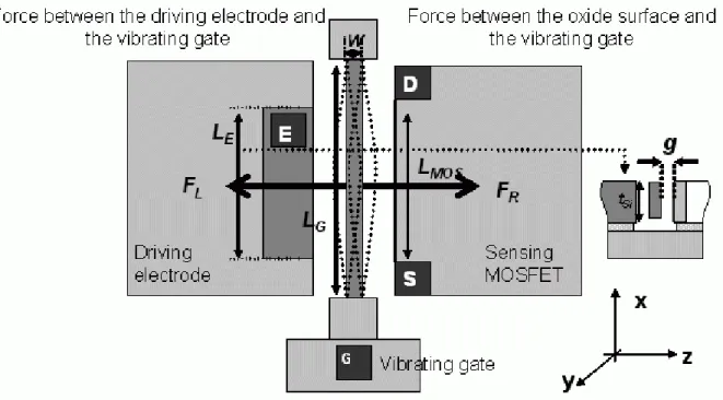
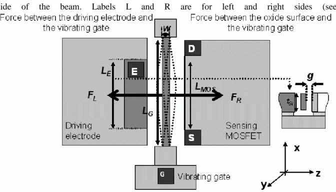
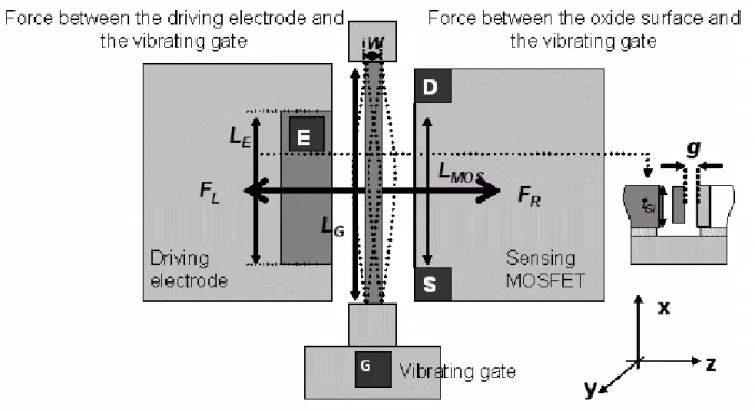
The geometry of the component and the notations are showed in the Figure 1
Figure . Second Newton equation is applied in the Galilean referential frame of the substrate to the ensemble beam+MOSFET. The beam is assumed to follow Euler-Bernouilli equation [8]. The equation is reduced to its normalized lumped expansion on the first mode through the Galerkin method, which consists in writing the solution over an orthogonal modal base
{
χn(x)}
n=1,∞:The cubic term α3 is the Duffing effect, Q is the quality factor, ω1 is the free resonance
frequency of the first mode. FR and F correspond to the electrostatic forces acting on each L
(
FR FL)
z Q z z z + + 3 + 1 1 = − 1 3 1 2 1 1 & & &ω
α
ω
(1)side of the beam. Labels L and R are for left and right sides (see
Figure).
{
χ
n(x)}
n=1,∞ follows the normalisation condition:nm L m n x x dx S G δ χ χ ρ =
∫
0 ) ( ) ( (2)The electrostatic force densities are projected on
χ
1(x):dx x z C V F E L L L L
∫
∂ ∂ = 0 1 1 2 ) ( 2χ
with VL =Vg −VE (3)∫
∂∂ = MOS L R R R x dx z C V F 0 1 1 2 ) ( 2 1χ
with VR =Vg −Voxide(z(x)) (4)Vg, VE, Voxide are respectively the gate voltage, the electrode voltage and the voltage between the surface of the oxide and the ground. CL and CR are the air gap capacitances per length
unit: )) ( ( ) ( 0 , x z g t C x CLR n Si ± = ε (5) 0
R
F is a bit more complex than FL because the potential difference depends explicitly on z(x)
through Voxide, which depends on the capacitive bridge
R MOS g
C C
V 1+ . The classical MOSFET
equations for each z-displacement are used to define CMOS.
First, the surface potential ϕs(x) is computed with an explicit model, which is obtained by asymptotic simplifications of the implicit equation for each operating regime [10]:
− + − + − − + = − − T k V q T k q q T k T k q q T k V V B Fi B s B B s B s s FB g ( 2 ) exp 1 exp 1 exp 2
φ
ϕ
ϕ
ϕ
γ
ϕ
(6) 2 0 2 i a Si C N qε
ε
γ
= , where 1 1 − + = R ox ox i C t Cε
Ci is the dielectric capacitance due to the oxide layer and the variable air gap.
(
s Fi)
i ss i i ms FB C Q C QV =
φ
− −ϕ
−φ
is the flat band voltage. Qi and Qss are respectively the chargedensity in the gate oxide and the charge density at the interface oxide / silicon. V(x) is the potential in the channel depending on Vds. q, Na,
ε
Si, kB, T andφ
Fi are respectively the electroncharge, the doping level of the channel, the relative dielectric permittivity, the Boltzmann constant, the temperature and the Fermi potential.
Once
ϕ
s known, the charge densities in the MOSFET and the MOS capacitance can be evaluated to determine oxide voltage and drain current:(
)
)) ( ( ) ( 1 ) ( exp ) ( ) ( x V V C x Q V V V V T k x q q T k x C x Q FB g FB g B s B S i dep − − − = − − − − + − = ϕ ϕ ϕ γ (7) 1 1 ) ( ; ) ( ) ( − + = ∂ ∂ = ox ox sc MOS s sc sc t C x C x Q x Cε
ϕ
(8)Where,Qdep(x), Qinv(x)and Qsc(x) are respectively the depletion charge density, the inversion charge density and the charge density in the gate. The drain current is the sum of the inversion charge density along the channel.
∫
− = d s V V inv eff Q V dV L W Id µ ( ) (9)µeff is the effective mobility of electron (N-MOSFET). For each operating point (Vg, Vds), µeff
is approximated by the Mathiessen rule considering the phonon interaction, the Coulomb interaction and the surface scattering [11].
Finally, the model depends on the geometry and a set of physical parameters (µeff,
Qi, Qss and Na). The equations (1) to (8) have to be solved self consistently through a robust iterative algorithm based on the Runge-Kutta formulation.
To validate our theoretical model, we compare the simulation results with measurements reported in [12]. Devices were fabricated with a technology based on 200mm tools with a SON (Silicon on Nothing) approach [7]. This technology takes advantage of the single-crystal silicon for the NEMS structure without using SOI wafers. This technology is compatible with a front-end CMOS process. The Figure 2 shows a SEM micrograph of a typical device.
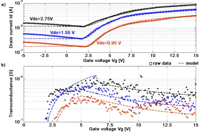
Let us consider a device (Figure 2) on which static measurement were carried out. The measured characteristics are LG=16.1 µm, w=490 nm, g=107 nm, LMOS= 9 µm,
WMOS=400 nm, tox=2 nm, and Na= 5.1015 at/cm3 [12]. Figure 3 a) and b)give respectively the
static characteristics Id(Vg) and gm(Vg) with VE=VS=0. The theoretical results are superimposed in each case. Notice that the bulk voltage (body potential) remains floating. To fit the model with the experimental results, the doping level Na, and the charge density in the gate oxide Qi are respectively fixed at 4.5.1015 at/cm3 and 5.1010 cm-2 since the charge density Qos at the
interface oxide / silicon is tuned. This parameter depends on the technology (etching step and oxide deposition) as well as the voltages. In the Figure 3 a), theory and measurement are well in agreement. Threshold voltages are quite similar around 2 V. Below the threshold, in the accumulation regime, the experimental device exhibits a quite strong leakage current from 0.1 µm to1.3µA. This current variation depends linearly on Vds at Vg=0V. It may be attributed to a photolithography misalignment when protecting channel from phosphorous implants generating a 2.1 MΩ short-circuit resistor. This process error can not be reproduced by the model and the resistance was added by hand in parallel of the transistor. For Vds=1.55V and 2.75V, the charge density Qss is respectively fixed at 1012 cm-2 and 1013 cm-2. The charge traps at the interface oxide / etched silicon may be gradually filled according to the surface potential, which depends both on Vgs and Vds. This additional charge induces a modification of the flat band voltage and the vertical electrical field leading to both threshold voltage variation and slop variation. In the Figure 3Figure b), we observe a quite large dispersion of raw data which makes the comparison difficult. Anyway, the computed values are in the good order of magnitude. The maximum of transconductance, is around 1 µS for (Vg=6.5V, Vds=2.75V) leading to an Id current of about 3 µA. For this operating point, µeff was evaluated at 300 cm2 /V.s.
Let us consider a device on which dynamic resonance were observed. The measured characteristics are LG=10 µm, w=165 nm, g=120 nm, LMOS= 6.8 µm, WMOS=400 nm, tox=2 nm,
and Na= 5.1015 at/cm3 [12]. RF characterizations were performed using a measurement bench
with a vectorial network analyser Agilent 8753E (VNA) to measure the S12 parameter (ratio of
the transmitted power over the incident power in the logarithmic scale). The values of the bias voltages applied on the component were extracted from the static characteristics Id(Vg) and
Id(Vds). Electrode voltage Vdc, gate voltage Vg and drain voltage Vds were respectively Vdc=10V,
4.5 mV RMS over 50 Ω). Pressure was fixed at 10-6 Torr – The quality factor Q was evaluated to ~700 that seems to be a typical value for such a vibrating beam. Our AC-simulation is based on the model presented in precedent section considering the experimental operating point. The total noise floor of the measurement chain loaded with the component is calculated to know the theoretical background level of the S12 parameter. This noise results from three main noise
sources (uncorrelated noise assumption): the white mechanical noise of the beam, the thermal noise current of the MOSFET and the VNA noise. The mechanical noise is computed using theoretical characteristics of the beam. The electrical noise is computed from the transconductance gm, and the source gate capacitance Cgs with our electrical model. gm, Cgs and
µeff are respectively evaluated at 200 nS, 0.2 fF and 100 cm2/V.s. The VNA noise is known through an open loop calibration without device (~380 pA/√Hz). Theoretical results and measurements are shown in the Figure 4. The model is well in agreement with the experiment despite the only use of physical parameters. The theoretical resonance frequency is quite close to the experimental frequency. The difference between the theoretical level and the measured level is only of 1 dB higher. The background shown in the Figure 4 is only due to the VNA. A low distortion of the experimental resonance peak, which is not anticipated by the model, is also visible. Its origin is not yet explained.
We detailed a unified electromechanical model for a LRG-MOSFET only based on physical assumptions. No any extra mathematical parameters to fit the behavior of the device are thus required. For static study, theory seems to be quite well in agreement with the measurement. The visible dispersion might be a poor control at the bulk potential because the body of the MOSFET was kept floating. Other reasons could be a strong surface density of charge traps and a strong roughness of the interface silicon/oxide inducing a large instability of the measurements. Next generation of component is in progress to improve the field effect and
the responsivity to the beam movement. Thus, the gap and the channel length are scaled down. A bulk pad is added to avoid any body effect. The gap reduction implies to take into account the Casimir force [13] that may have an impact at tiny gap. This force is already included in the model. Compared with other models, our model is more comprehensive since it computes the charges densities in the channel according to the mechanical oscillations. It may finally be suitable for any electromechanical components based on a field effect transduction.
[1] H.C. Nathanson, W.E. Newell, R. A. Wickstrom and J.R. Davis, IEEE Transactions on. Electron Devices., Vol. ED-14, No.3, 117-133 (1967).
[2] N. Yazdi, F. Ayazi, andK. Najafi, Proceedings of the IEEE, Vol. 86, No 8, 640-1659 (1998).
[3] M.L. Roukes, Physics World, Vol. 14 No 2, 25-31 (2001)
[4] K. L. Ekinci, Y. T. Yang and M. L. Roukes, Journal of Applied Physics, Vol. 95, No 5, 2682-2689 (2004).
[5] B. Ilic, Y. Yang, and H. G. Craighead, Applied Physics Letters 85, No 13, 2604-2606 (2004).
[6] E. Ollier, L. Duraffourg, MT. Delaye, H. Grange, S. Deneuville, J. Bernos, R. Dianoux, F. Marchi, D. Renaud, T. Baron, P. Andreucci, P. Robert, IEEE-NEMS 07, Bangkok, Thailand, January 16-19 (2007); S. Monfray, T.S. Skotnicki, Y. Morand, S. Descombes, M. Paoli, P. Ribot, A. Talbot, D. Dutartre, F. Leverd, Y. Lefriec, R. Pantel, M. Haond, D. Renaud, M.E. Nier, C. Vizioz, D. Louis, N. Buffet IEDM, Washington DC, USA, 2971-2974, December 3-5 (2001)
[7] N. Abelé, V. Pott, K. Boucart, F. Casset, K. Segueni, P. Ancey, A.M. Ionescu, Electronics Letters, Vol. 41, No 5 (2005)
[9] Nishiyama H. and Nakamura K., IEEE Transaction on Components, Hybrids, and Manufacturing Technology, Vol. 13, No. 2 (1990).
[10] S.B. Chiah, X. Zhou, K. Chandrasekaran, W.Z. Shangguan, G.H. See and S.M. Pandey, Applied Physics Letters 86, 202111 (2005).
[11] C. Lombardi, S. Manzini, A. Saporito and M. Vanzi , IEEE Transaction on Computer-Aided Design, Vol. 7, No. 11 (1988).
[12] C. Durand, V. Pott, K. Boucart, F. Casset, K. Segueni, P. Ancey, A.M. Ionescu, Accepted in Electron Device Letters, to be published in May 2008.
Figure 1: Schematic of the LRG-MOSFET – FL and FR are the electrostatic forces on each side of the vibrating gate – LE and LMOS are respectively the electrode length and the channel length – g is the air gap – tSi is the thickness of the top layer – w is the gate width.
Figure 3: Static characteristics of the LRG-MOSFET – a) Id(Vg) – b) Transconduction
gm(Vg).