Effect of MOSFET Threshold Voltage Variation on High-Performance Circuits
bySiva G. Narendra
Bachelor of Engineering in Electronics and Communication Engineering Government College of Technology, Coimbatore, India, June 1992.
Master of Science in Computer Engineering Syracuse University, Syracuse, NY, June 1994.
Submitted to the Department of Electrical Engineering and Computer Science in Partial Fulfillment of the Requirements for the Degree of
Doctor of Philosophy in Electrical Engineering and Computer Science at the
Massachusetts Institute of Technology January 2002
© 2002 Siva G. Narendra. All rights reserved.
The author hereby grants to MIT permission to reproduce and to distribute publicly paper and electronic copies of this thesis document in whole or in part.
Signature of Author
Department of 81WieiMT ngineering and Computer Science A January 31, 2002 Certified by
Anantha ('handrakasan, Ph.D. Associate Professor of Electrical Engineering Thesis Supervisor Certified by Dimitri Antoniadis, Ph.D. Professor of Electrical-Engineering Thes, iipervi's6r Accepted by
Arthur Smith, Pih. Professor of Electrical Engineering
Graduate Officer MASSACHUSETTS INSTITUTE OF TECHNOLOGY 1
APR 16
2002
BARKER
LIBRARIES
Effect of MOSFET Threshold Voltage Variation on High-Performance Circuits by
Siva G. Narendra
Submitted to the Department of Electrical Engineering and Computer Science on January 31, 2002 in partial fulfillment of the requirements for the degree of
Doctor of Philosophy in Electrical Engineering and Computer Science Abstract
The driving force for the semiconductor industry growth has been the elegant scaling nature of CMOS technology. In future CMOS technology generations, supply and threshold voltages will have to continually scale to sustain performance increase, limit energy consumption, control power dissipation, and maintain reliability. These continual scaling requirements on supply and threshold voltages pose several technology and circuit design challenges. One such challenge is the expected increase in threshold voltage variation due to worsening short channel effect. This thesis will address three specific circuit design challenges arising from increased threshold voltage variation and present prospective solutions. First, with supply voltage scaling, control of die-to-die threshold
voltage variation becomes critical for maintaining high yield. An analytical model will be
developed for existing circuit technique that adaptively biases the body terminal of MOSFET devices to control this threshold voltage variation. Based on this model, recommendations on how to effectively use the technique in future technologies will be presented. Second, with threshold voltage scaling, sub-threshold leakage power is expected to be a significant portion of total power in future CMOS systems. Therefore, it becomes imperative to accurately predict and minimize leakage power of such systems, especially with increasing within-die threshold voltage variation. A model that predicts system leakage based on first principles will be presented and a circuit technique to reduce system leakage without reducing system performance will be discussed. Finally, due to different processing steps and short channel effects, threshold voltage of devices of same or different polarities in the same neighborhood may not be matched. This will introduce mismatch in the device drive currents that will not be acceptable in some high performance circuits. In the last part of the thesis, voltage and current biasing schemes that minimize the impact
of neighborhood threshold voltage mismatch will be introduced. Thesis Supervisor: Anantha Chandrakasan
Title: Associate Professor of Electrical Engineering Thesis Supervisor: Dimitri Antoniadis
Title: Professor of Electrical Engineering Thesis Supervisor: Vivek De
Title: Principal Engineer, Intel Corporation Thesis Reader: Charles Sodini
Title: Professor of Electrical Engineering
To Appa.. .for proving that learning never ceases,
and to Amma.. .for teaching the art of learning.
Acknowledgements
Throughout the course of implementing this work, I had the privilege of interacting with some of the best in the field of electrical engineering, for which I am very grateful. Foremost, I am indebted to my thesis advisors - Prof. Anantha Chandrakasan, for his vision and motivation in guiding me to explore the bridge between devices and circuits; Prof. Dimitri Antoniadis, for being a patient and inspiring teacher; and Dr. Vivek De of Intel Labs, for being an invaluable technical mentor. I am also extremely grateful for their trust in the choices I made to complete this thesis.
I want to thank Prof. Charles Sodini for his time, encouragement, and technical guidance. I would like to express my gratitude to several EECS faculty members, especially, Prof. Duane Boning, Prof. Don Troxel, Prof. Clifton Fonstad, Prof. Jesus delAlamo, Prof. Judy Hoyt, and Prof. Raphael Reif for their valuable support. My stay at MIT was stimulating and entertaining, thanks to the friendship of Dr. Kush Gulati, Dr. James Kao, Dr. Andy Wei, Dr. Isabel Yang, Dr. Mark Armstrong, Dr. Anthony Lochtefeld, Dr. Keith Jackson, Jeremy Milikow, and Prasanth Duvvur. I also would like to acknowledge Marilyn Pierce at the EECS graduate office and Margaret Flaherty for their help in getting this thesis in order.
I am appreciative of the support from all of my colleagues at Intel Labs. Specifically, Brad Bloechel, Jim Tschanz, Matt Haycock, and Greg Dermer for their invaluable support in the lab; Shekhar Borkar, Richard Hofsheier, and Justin Rattner for their technical leadership and for funding this research; Nitin Borkar and team for the coffee breaks, guidance in design, and for silicon real-estate. I am also grateful to Dr. Soumyanath Krishnamurthy for energizing me to complete the research and to Dr. Ali Keshavarzi, Dr. Yibin Ye, and Dr. Dinesh Somasekhar for numerous technical discussions. Many thanks to Greg Ruhl, Dan Klowden, and Zachary Keer for their interest and participation.
All of this was made possible by the love and encouragement of my family. I am deeply indebted to my parents, Dr. M. R. P. Gurusami and Varamani, for teaching me the value in accumulating the wealth of knowledge. I am also very fortunate to have the collective guidance of five older siblings, Nallini, Madhavi, Ezhil, Aravanan, and Senthil. Each sibling and their family have an irreplaceable influence in my life, for which I am very grateful. I want to acknowledge my parents-in-law, Ashok and Meena, and sister-in-law Aditi for their support. Thanks to Inji for her playful company during the process of writing this thesis. Finally, I am exceedingly thankful for the immense love and friendship from my soul mate Monika.
Contents
Chapter 1
Introduction ...
21
1.1 Thesis organization ... 24
Chapter 2
Background...25
2.1 Technology scaling and threshold voltage variation... 25
2.2 Threshold voltage variation categories ... 29
Chapter 3
Die-to-die and Within-die Threshold Voltage Variations...33
3.1 Adaptive body bias ... 33
3.1.1 Adaptive body bias and short channel effect (SCE)... 34
3.1.2 Scaling of required body bias and SCE increase... 33
3.1.3 Impact on within-die threshold voltage variation... 41
3.1.4 Summary ... 43
3.2 Bi-directional adaptive body bias ... 43
3.3 Body bias circuit impedance requirement... 50
Chapter 4
Within-die Threshold Voltage Variation and Leakage Power...57
4.1 Estimation of chip leakage current... 57
4.1.1 Present leakage current estimation techniques ... 57
4.1.2 Leakage current estimation including within-die variation ... 58
4.1.3 M easurement results... 61
4.2 Leakage reduction... 62
4.2.1 M odel for stack effect factor ... 64
4.2.2 Leakage reduction using forced-stacks... 69
4.2.3 Stack effect vs. channel length increase ... 71
4.2.4 Case study and summ ary... 73
Chapter 5 Neighborhood Threshold Voltage Variation...75
5.1 Voltage biasing ... 76
5.1.1 Application of voltage bias to low-voltage sense-am plifiers ... 77
5.2 Current biasing...81
5.2.1 Basic iso-current biasing and two-phase clock generation... 81
5.2.2 Process insensitive current biasing... 84
5.2.2.1 Process insensitive constant current generation... 85
Chapter 6 Conclusion... 91
6.1 Contributions...91
6.2 Suggestions for future work... 93
Bibliography...95
List of Figures
Figure 1-1: Timeline on technology scaling and new microprocessor architecture introduction. ... 22 Figure 1-2: Basic form of M oore's law... 22 Figure 1-3: Relative die sizes of the last nine microprocessor generations...23 Figure 2-1: Barrier height lowering due to channel length reduction and drain voltage increase in
an nM O S ... 26 Figure 2-2: Barrier lowering (BL) resulting in threshold voltage roll-off with channel length
reduction. Drain induced barrier lowering (DIBL) reduces threshold voltage for short channel devices and increases threshold voltage roll-off. For short channel devices channel length variation (AL) translates to threshold voltage variation (AVT)...26
Figure 2-3: Dependence of threshold voltage variation on channel length and drain voltage; n is the number of MOS device samples measured. ... 27 Figure 2-4: Relationship between threshold voltage (Vt) and sub-threshold leakage current (Ioff).27 Figure 2-5: Trend in sub-threshold leakage and switching power with technology scaling. ... 28 Figure 2-6: Threshold voltage variation categories covered in the thesis. ... 30 Figure 3-1: Die-to-die threshold voltage distributions (a) Conventional approach without adaptive
body bias (b) Adaptive body bias approach. ... 33 Figure 3-2: Reduction in Vt modulation with reverse body bias with reduction in Vt...35 Figure 3-3: Increase in Vt-roll-off with Vt reduction and reverse body bias increase...35
Figure 3-4: Increase in DIBL due to increase in reverse body bias...36 Figure 3-5: (a) Adaptive body bias reduces the die-to-die Vt variation. (b) Within-die Vt variation
increases for die samples that require body bias to match their mean Vt to the target Vt.
Vt-target is the target saturation threshold voltage for a given technology. Vt-low and Vt-nom are the minimum and mean threshold voltages of the die-to-die distribution...38 Figure 3-6: Trend in mean saturation threshold voltage of different die samples before adaptive body bias under (a) 30% Vt scaling and (b) 20% Vt scaling scenarios...40 Figure 3-7: Matching of mean saturation threshold voltages of different die samples with adaptive
body bias under (a) 30% Vt scaling and (b) 20% Vt scaling scenarios...40 Figure 3-8: Increase in within-die threshold voltage variation due to increase in short channel
effect with adaptive body bias under (a) 30% Vt scaling and (b) 20% Vt scaling. We assume that the dominant reason for within-die Vt variation is critical dimension variation. The results shown here assume within-die variation in Lg of 5%...42 Figure 3-9: Die-to-die threshold voltage distributions (a) Conventional approach without adaptive
body bias (b) traditional adaptive body bias approach - die sample that requires maximum reverse body bias is 2AVt2 away from Vt-target (c) bi-directional adaptive body bias approach - die sample that requires maximum reverse body bias is AVtl away from
Vt-target. Note: AVt2 > AVtl since SCE of devices with lower Vt will be more. ... 44 Figure 3-10: Chip micrograph of a sub-site... 45 Figure 3-11: Circuit block diagram of each sub-site ... 46 Figure 3-12: Demonstration of frequency adapting to meet target and list of possible on-chip bias
m o des...4 6
Figure 3-13: Die-to-die variation in frequency and leakage for no body bias (NBB), 0.2 V static forward body bias (FBB), and adaptive body bias applied to compensate die-to-die
variation (A B B )...47
Figure 3-14: Frequency vs. number of critical paths that determine the frequency...47
Figure 3-15: Comparison of variations in within-die device current and frequency...48
Figure 3-16: Die-to-die variation in frequency and leakage for adaptive body bias applied to (i) compensate die-to-die variation (ABB) and (ii) compensate within-die variation (WID-A B B )...4 9 Figure 3-17: Histogram of bias voltages within a die sample and effect of bias resolution on frequency distribution... 50
Figure 3-18: Communications router chip architecture with PMOS body bias. ... 51
Figure 3-19: Measurement of body and Vcc current...51
Figure 3-20: Overview of body bias generation and distribution...52
Figure 3-21: Buffer impedance requirements and body bias noise comparisons with NBB...53
Figure 3-22: LBG buffer implementations and comparisons... 54
Figure 3-23: Frequency vs. Vcc of FBB and NBB chips...55
Figure 3-24: Leakage reduction from active to standby mode in FBB chips...56
Figure 3-25: Micrograph of communications router chip with PMOS body bias and of chip characteristics. ... 56
Figure 4-1: Comparison of calculated leakage versus measured leakage for (a) existing leakage current estimation techniques and (b) leakage current estimation technique introduced in th is thesis...6 1 Figure 4-2: Ratio of measured to calculated leakage current ratio distribution for Ieak-, IleA-I, and eak-, techniques (Sam ple size: 960)... 61
Figure 4-3: Leakage current difference between a single off device and a stack of two off devices. As illustrated by the energy band diagram, the barrier height is modulated to be higher for the two-stack due to smaller drain-to-source voltage resulting in reduced leakage...62 Figure 4-4: Trade-off between standby leakage and performance by forcing a two-stack under iso-input load. An NMOS two-stack will reduce leakage when iso-input stays at logic "0"...63 Figure 4-5: Load line analysis showing the leakage reduction in a two-stack...65 Figure 4-6: Measurement results showing the relationship between stack effect factor X for a
two-stack to the universal exponent U. Lines indicate the relationship as per the analytical model and symbols are from measurement results. White symbols are for nominal channel devices and gray symbols are for devices smaller than the nominal channel length. Triangle, circle, and square symbols are for Vdd of 1.5, 1.2, and 1.1 V respectively. Zero
body bias is when the body-to-source diode of the device closet to the power supply is zero biased and reverse body bias is when the diode is reverse biased by 0.5 V...66 Figure 4-7: Measurement results indicate a slower rate of increase in leakage of two-stack
compared to that of a single device. This should translate to reduction in the variation of effective threshold voltage. ... 67 Figure 4-8: Nominal channel length device measurement results showing stack effect factor across
two technology generations. The increase in stack effect factor is attributed to worsening of short channel effect, Ad, which is predicted by the analytical model. The higher stack effect
factor for the low-V, device in 0.13-pm technology generation is attributed to the same
reason. Lines are from analytical model and symbols are from measurement...67 Figure 4-9: Nominal channel length device measurement results indicating the scaling of stack
effect factor from 0.18jim to 0.13gm low-V, under different Vdd scaling conditions. The
low-V, device will dominate leakage in 0.13gm technology, so the comparison is made w ith the low -V, device ... 68 Figure 4-10: Prediction in the scaling of stack effect factor for two Vdd scaling scenarios in
nominal channel length devices. Vdd for 0. 18gm is assumed to be 1.8 V...68 Figure 4-11: Stack forcing and dual-V, can reduce leakage of gates in paths that are faster than
req u ired ... 69 Figure 4-12: Simulation result showing the nominal channel length delay versus mean leakage trade-off that can be achieved by stack forcing technique under iso-input load conditions. Iso-input load is achieved by making the gate area after stack forcing identical to before stack forcing. Several such conditions are possible, which enhances delay-leakage trade-off possible by stack forcing. The two-stack condition with the least delay is for w,=w=2w.
This trade-off can be used with or without high-V, transistors...70 Figure 4-13: A sample path where natural stack is used to reduce standby leakage by applying a
predetermined vector during standby. No delay penalty is incurred with this technique...70 Figure 4-14: Using stack-forcing technique the number of logic gates in stack mode can be increased. This will enable further leakage reduction in standby mode. Increase in delay under normal mode of operation will be incurred ... 71 Figure 4-15: If a gate can have its input as either "0" or "1" and still force stack effect then that
gate will have reduced active leakage. The more the number of inputs that can be either "0" or "1" the higher the probability that stack effect will reduce active leakage...71 Figure 4-16: Comparing device leakage reduction due to channel length increase with two-stack
leakage. The channel length is given by il x 0.18 [im. Stack leakage is a two stack of
devices with ij=1 and wu=wl=%w. Leakage numbers are obtained from simulation under
iso-input load ... 72
Figure 4-17: Energy-delay trade-off of inverter under different configurations with fan-out of 1 and iso-input load. The simulation-based comparison clearly shows that the two-stack configuration's delay is less than increasing channel length, especially when compared to
iso-standby leakage (Ti=3) configuration... 72
Figure 4-18: Summary of delay-leakage trade-off comparison between two-stack and channel len gth ... 7 3 Figure 5-1: Die-micrograph of mismatch structures testchip...76
Figure 5-2: Linear threshold voltage mismatch for 500 mV forward body bias, zero body bias and 500 m V reverse body bias ... 77
Figure 5-3: Traditional sense-amplifier... 78
Figure 5-4: Body voltage for the traditional sense-amplifier. ... 78
Figure 5-5: Dependence of saturation threshold voltage mismatch on body bias... 79
Figure 5-6: New no body bias sense-amplifier...79
Figure 5-7: Total delay verses input differential for iso-output differential at 1.5 V, 1 mV/pS ramp rate, and 110 Celsius, for the traditional and the new sense-amplifiers... 79
Figure 5-8: Total delay (sense-amplifier delay plus ramp development delay) improvement due to input offset reduction in the new sense-amplifier at 1.5 V, I mV/pS ramp rate and
110
C elsiu s. ... 80Figure 5-9: Basic iso-current biasing scheme ... 82
Figure 5-10: Standard two-phase clock generator design ... 82
Figure 5-11: Iso-bias current based non-overlapping two-phase clock generator... 83
Figure 5-12: Performance comparison of two-phase generators... 84
Figure 5-14: Measured process variation in a long-channel, wide-width, process-uncompensated, device current (I). Measurements were carried out across wafer on identical devices with 0.9 V gate drive. Both raw data and statistical information are presented above...87 Figure 5-15: Normalized process variation in If for different device size ratios when a=2 and b=5.
Measurement confirms process variation in If minimizes at zJ/z2 ratio predicted by the theoretical m odel...88
Figure 5-16: Measured variation in If for a=2, b=5, and zJ/z2=1/8. Device current and V, measurements were carried out across wafer on two devices with appropriate gate drives and device sizes given by the theoretical model... 88 Figure 5-17: Circuit schematics showing generation of V, and I,f. Since generated V, will not be accurate, device size ratio zl/z2 was optimized with a=2, b=5 and Vdd=0.9 V to minimize
Ire/s process variation... 89
Figure 5-18: Circuit simulation results with a=2, b=5, zl/z2=1/6, Vdd=0.9 V, showing variation in I, and Iref. With respect to typical process corner I, varied by +22% and -16% while variation in Iref was -5% and -5%. Total variation in normalized I, across all process corners is 0.38 while it is 0.05 for norm alized Iref. ... 89
List of Tables
Table 3-1: Technology parameters under two scaling scenarios... 37 Table 3-2: With adaptive body bias short channel effect of devices increase, indicated by DIBL (Ad
in mV/V) increase and body effect reduction factor (11) decrease. This SCE increase is worse for Vt-low devices, compared to Vt-nom devices, as they require larger body bias to match Vt-target. The required bias values (in V) are indicated within parentheses...41 Table 5-1: Total delay improvement under different supply voltage and ramp rate conditions for
input differential of 150 mV for the traditional sense-amplifier and 118 mV for the new zero body bias sense-amplifier at 110 Celsius. Larger improvement is correlated to faster sense-amplifier resulting in input offset and ramp development delay reductions more critical...80
Table 5-2: Sub-set of parameters that satisfy equations (6)-(7) to minimize process impact on Ief = 1 1 - I2...87
Table 5-3: Low voltage operation enabled by redesigning Vt generation circuit...90
Chapter 1
Introduction
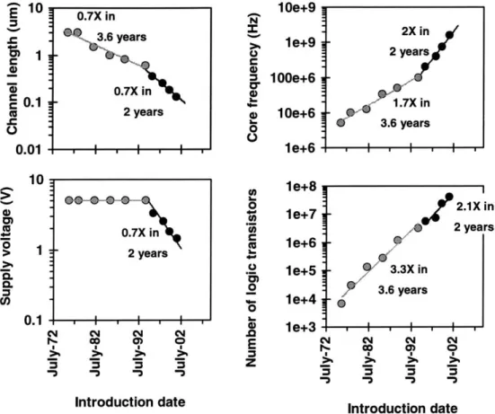
MOS transistor based integrated circuits have transformed the world we live in. It is estimated that there are more than 15 billion silicon semiconductor chips currently in use with an additional 500,000 sold each day [1]. The ever shrinking size of the MOS transistors that result in faster, smaller, and cheaper systems have enabled ubiquitous use of these chips. Among these semiconductor chips, a prevalent component is the high-performance general-purpose microprocessor. Figure 1-1 illustrates the timeline on technology scaling and new high-performance microprocessor architecture introductions in the past three decades [2]. This trend holds in general for other segments of the semiconductor industry as predicted by Moore's law [3]. In 1965, Gordon Moore showed that for any MOS transistor technology there exists a minimum cost that maximizes the number of components per integrated circuits. He also showed as transistor dimensions are shrunk (or scaled) from one technology generation to the next, the minimal cost point allows significant increase of the number of components per integrated circuit as shown in Figure 1-2.
Historically, technology scaling resulted in scaling of vertical and lateral dimensions by 0.7X each generation resulting in delay of the logic gates to be scaled by 0.7X and the integration density of logic gates to be increased by 2X. From the timeline shown in Figure 1-1 it is clear that there were two distinct eras in technology scaling - constant voltage scaling and constant electric field scaling.
Constant voltage scaling era (First two decades): Technology scaling and new architectural introduction in this era happened every 3.6 years. Technology scaling should scale delay by 0.7X translating to 1.4X higher frequency. However, frequency scaled by 1.7X with the additional
increase primarily brought about by increase in the number of logic transistors. As it can be seen from Figure 1-1 the number of logic transistors increased by 3.3X in each of the new introductions. Technology scaling itself would have provided only 2X - the additional increase was enabled by increase in die area of about 1.5X every generation [4].
E 10 1 Oe+9 E OX in 0 2X in . .
3.6
years3.6 CIc
2 years S100e+6
Z in e+.7X S0.1 - :1.7X in 2 years 1 1e+6 -3.6 years 0 1 e+8 0 2.1X in " 1 e+7-c.7ci 2 years 0 1 e+600
> 2 years 1 e+5 -3.3X in )"3.6 years Cn Ie+4 0.1 II I- 0Introduction date Introduction date
Figure 1-1: Timeline on technology scaling and new microprocessor architecture introduction.
Figure 1-2: Basic form of Moore's law.
22 Er-'&P 7 - - --.. ' --- - - - 7-
',--Constant electric field scaling era (Past decade): Technology scaling and new architectural introduction in this era happened every 2 years along with voltage scaling of 0.7X. As always technology scaling should scale delay by 0.7X translating to 1.4X higher frequency, but frequency increased by 2X in each new introduction. The additional increase in frequency was primarily brought by decrease in logic depth through architectural and circuit design advancements. The number of logic transistors grew only by about 2.lX every generation, which could be achieved without significant increase in die area. Since switching power is proportional to Area x s/distance x Vdd x Vdd x F, it increased by (1 x 1/0.7 x 0.7 x 0.7 x 2 =) 1.4X every generation. Although the die size growth is not required for logic transistor integration, it is important to note that the total die area did continue to grow at the rate of 1.5X per generation [4] due to increase amount of integrated memory. Relative die areas for the last nine microprocessor generations are shown in Figure 1-3.
Figure 1-3: Relative die sizes of the last nine microprocessor generations.
In the past decade, technology and new architecture product cycles reduced from 3.6 years to 2 years. From an operational perspective, this requires concurrent engineering in product design, process design, and manufacturing supply lines [5]. The past decade also required supply voltage scaling imposed by oxide reliability and the need to slow down the switching power growth rate. From the process design stand point supply voltage scaling requires threshold voltage scaling [6, 7] so that the technology scaling can continue to provide 1.4X frequency increase. To prolong the tremendous growth the industry has experienced in the past three decades threshold voltage scaling and concurrent engineering has to continue. These requirements pose several challenges in the coming years including increase in process variation, worsening interconnect RC delay, and increase in sub-threshold, gate, and tunneling leakage components [7, 8]. This thesis will focus on one of the challenges - the increasing importance of threshold voltage variation and how it impacts digital CMOS circuits used in microprocessors and other high-performance integrated circuits.
1.1 Thesis organization
In the subsequent chapters the effects of MOSFET threshold voltage variation on the leakage power, delay, and operation of high-performance digital CMOS circuits, and potential circuit solutions that alleviate these effects will be presented in the following order:
* Chapter 2 provides a brief background on the reasons for the increasing importance of threshold voltage variation, existing solutions, and a detailed overview of the research concepts investigated in this thesis.
" Chapter 3 focuses on different aspects of die-to-die threshold voltage variation and its impact on delay and power of the integrated circuit. Ineffectiveness of prior published circuit solution to minimize die-to-die threshold voltage variation as technology scales and the detrimental interaction this solution introduces between die-to-die and within-die threshold voltage variations are identified. An improved circuit solution that is void of these defects is described.
* Chapter 4 introduces (i) the importance of taking into account the influence within-die threshold voltage variation will have on system's leakage power especially as technology scales and (ii) a circuit technique to reduce system leakage power.
* Chapter 5 describes circuit techniques to reduce the impact threshold voltage mismatch between MOS devices in the same neighborhood.
* Summary of this work is described in Chapter 6. Suggestions for future work are also discussed in Chapter 6.
Chapter 2
Background
Conventionally, CMOS technology has been scaled to provide 30% smaller gate delay with 30% smaller dimensions, resulting in CMOS systems operating at about 40% higher frequency in half the area with reduced energy consumption. Scaled CMOS systems, such as new generation microprocessors, achieve at least an additional 60% frequency increase with augmented architecture and circuit techniques. This complexity increase results in higher energy consumption, peak power dissipation and power delivery requirements [4].
To limit the energy and power increase in future CMOS technology generations supply voltage will have to continually scale. The amount of energy reduction depends on the magnitude of supply voltage scaling [9]. Along with supply voltage scaling, MOSFET device threshold voltage will have to scale to sustain the traditional 30% gate delay reduction. This supply and threshold voltage scaling requirements pose several technology and circuit design challenges [4, 8, 10]. One such challenge is the expected increase in threshold voltage variation due to worsening short channel effects. This is explained in the following section.
2.1 Technology scaling and threshold voltage variation
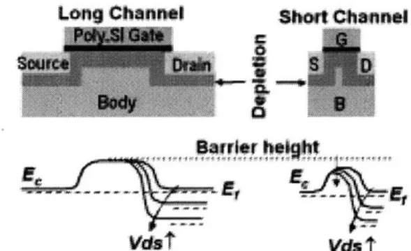
With technology scaling, the MOSFET's channel length is reduced. As the channel length approaches the source-body and drain-body depletion widths, the charge in the channel due to these parasitic diodes become comparable to the depletion charge due to the MOSFET gate-body voltage [11], rendering the gate and body terminals to be less effective. As the band diagram illustrates in Figure 2-1, the finite depletion width of the parasitic diodes do not influence the energy barrier height to be overcome for inversion formation in a long channel device. However, as the channel length becomes shorter both channel length and drain voltage reduce this barrier height. This
dimensional effect makes the barrier height to be modulated by channel length variation resulting in threshold voltage variation as shown in Figure 2-2. The amount of barrier height lowering, threshold voltage variation, and gate and body terminal's channel control loss will directly depend on the charge contribution percentage of the parasitic diodes to the total channel charge. Figure 2-3 shows measurements of 3a threshold voltage variations for three device lengths in a 0.18-gm technology confirming this behavior. It is essential to mention that in sub-micron technologies variation in several physical and process parameters lead to variation in the electrical behavior of the MOS device. The discussions in this thesis will address variation in the electrical behavior manifested as threshold voltage variation because of parameter variation. In addition, the threshold voltage variations addressed here are due to short channel effect in scaled MOS devices and not on threshold voltage variation due to random dopant fluctuation effect. Random dopant fluctuation effect is expected to be one of the significant sources of threshold voltage variation in devices of small area [12].
Long Chan".I ShW C$aw
VdST Vdst
Figure 2-1: Barrier height lowering due to channel length reduction and drain voltage increase in an nMOS.
V1LW,(Vo,4O
AV- -VTAT (VD.=VDOP
Channel length (um)
Figure 2-2: Barrier lowering (BL) resulting in threshold voltage roll-off with channel length reduction. Drain induced barrier lowering (DIBL) reduces threshold voltage for short channel devices and increases threshold
voltage roll-off. For short channel devices channel length variation (AL) translates to threshold voltage variation (AVT)
40 Vds: 5O mV 0 30- n: 10 >> 20 -0 1Da 0.18 0.36 0.72 L (jim)
Figure 2-3: Dependence of threshold voltage variation on channel length and drain voltage; n is the number
of MOS device samples measured.
It was mentioned in Chapter 1 that in order to maintain the performance increase trend with technology scaling threshold voltage would have to be scaled along with supply voltage. However, reduction in threshold voltage increases the sub-threshold leakage current significantly. Relationship between threshold voltage and sub-threshold leakage is illustrated in Figure 2-4. Typically, reduction in threshold voltage of about 85 mV, as shown in Figure 2-4, will increase the sub-threshold leakage current by lOX.
O
s
I
..
...
.
r 0.0010.00014
0.000001
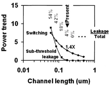
0 0.5 1 . Gate voltageAs indicated Chapter 1 switching power increases by 1.4X per generation. With scaling of threshold voltage sub-threshold leakage power will increase at a very rapid rate due to its strong dependence on the threshold voltage. Figure 2-5 illustrates the comparison between the increase in the switching power and sub-threshold leakage power with technology scaling. As it is evident from the figure sub-threshold leakage power will be comparable to the switching power in the immediate future. This 'inefficient' leakage power manifests itself as active leakage that influences the total power budget during operation and as standby leakage that influences the battery life of hand held systems. It therefore becomes important to not only reduce sub-threshold leakage power but also accurately estimate it.
Switching 1.4X Sub-threshold leakage
0.1
I - I~I ~*11111I
Channel length (um)
Figure 2-5: Trend in sub-threshold leakage and switching power with technology scaling.
28
15
-10
5
-0 a-L7
Leakage Total ft I U-r-0.01
With supply and threshold voltage scaling, control of threshold voltage variation becomes essential for achieving high yields and limiting worst-case leakage [13]. Maintaining good device aspect ratio, by scaling gate oxide thickness is important for controlling threshold voltage tolerances [7]. With the silicon dioxide gate dielectric thickness approaching scaling limits due rapid increase in gate tunneling leakage current [14, 15] researchers have been exploring several alternatives, including the use of high permittivity gate dielectric, metal gate, novel device structures and circuit based techniques [16, 17, 18, 19, 20, 21]. The use of high permittivity gate dielectric will result in thicker and easier to fabricate dielectric for iso-gate oxide capacitance with potential for significant reduction in gate leakage. Identification of a proper high permittivity dielectric material that has good interface states with silicon along with limited gate leakage is in progress [16]. However, it has also been shown that use of high permittivity gate dielectric has limited return [17]. Use of metal gate prevents poly-depletion resulting in a thinner effective gate dielectric. However, identification of dual metal gates to replace the n+ and p+ doped polysilicon is essential to maintain threshold voltage scaling. In addition, novel device structures such as self-aligned double gate planar MOSFETs provide better device aspect ratio [18]. Other than material
and device based solutions, circuit design solutions such as threshold canceling logic [19] and adaptive body bias [20, 21] enable supply and threshold voltage scaling. Threshold canceling logic mimics threshold voltage scaling by defining the MOS off state with IVgsI > 0, instead of IVgsI = 0. Although threshold canceling logic enables threshold voltage scaling, it requires larger area due to increase in logic complexity and number of power grids.
2.2
Threshold voltage variation categories
The three threshold voltage variation categories illustrated in Figure 2-6, which impact high-performance circuit design, will be covered in the next three chapters. In Chapter 3 of this thesis an analytical model will be developed, to show that traditional adaptive reverse body bias circuit solution to reduce die-to-die threshold voltage variation is not scalable for future generations and this technique results in increased within-die threshold voltage variation [22]. Use of bi-directional adaptive forward and reverse body bias to limit threshold voltage variation is more promising [23]. Forward body bias can be used not only to reduce threshold voltage [24, 25], but also to reduce die-to-die and within-die threshold voltage variations as will be shown in Chapter 3. Bias circuit impedance requirements for on-chip body bias are also discussed in Chapter 3.
It is important to note that threshold voltage variation not only affects supply voltage scaling but also the accuracy of leakage power estimation. Accurate leakage power estimation is very critical for future CMOS systems since the leakage power is expected to be a significant portion of the total power due to threshold voltage scaling [4]. In Chapter 4, leakage power estimation that takes into account within-die threshold voltage variation will be presented. In a leakage dominant CMOS system, it also becomes inevitable to identify techniques to reduce this variation and leakage power. In Chapter 4 the use of stacked devices to reduce system leakage power without reducing system performance will be shown. An analytical model to predict the scaling nature of this stack effect and verification of the model through statistical device measurements will be presented. Measurements also show reduction in threshold voltage variation for stacked devices compared to non-stack devices. Comparison of stack effect to the use of high threshold voltage or longer channel length devices for leakage reduction will also be discussed [26].
Chapter 5 of this thesis will deal with the variation in the threshold voltage of matched devices that are in the same neighborhood. The devices that are in close proximity can be either of the same polarity or of different polarity. Matched devices of the same polarity are used as sense-amplifier input devices for low voltage swing sensing among other applications [27]. Any mismatch in threshold voltage of this input device pair will appear as input offset resulting in degraded performance. A simple voltage-biasing scheme that reduces the mismatch between matched transistor pair of same polarity will be discussed.
Neighborhood threshold voltage mismatch Within-die threshold voltage variation Die-to-die threshold voltage variation
Figure 2-6: Threshold voltage variation categories covered in the thesis.
In addition, for some digital CMOS circuits a known PMOS to NMOS drive current ratio is required either to achieve a well-defined switching threshold or to achieve equal rising and falling delays. Since the processing steps such as threshold voltage implants for the PMOS and NMOS devices are not correlated there could be significant variation between the required and achieved threshold voltages for the two device types. The short channel effects further worsen this variation. The net variation will change the drive current ratio of PMOS to NMOS devices and can affect the operation of high performance circuits that depend on a pre-determined skew between the two device types. Ability to adjust the charging and discharging currents by sensing the skew difference can alleviate this problem. In Chapter 5 current biasing schemes that maintain the relationship between the charging and discharging currents, independent of the process skew is explained. The first current scheme that is the simplest, guarantees constant ratio between charging and discharging currents no matter the change in the relative skews of the PMOS and NMOS devices. Although this scheme maintains the relationship between charging and discharging delays, it doesn't provide constant delay as the threshold voltages vary. A true process insensitive current generation theory and circuit will be described in Chapter 5 [28]. This can then be used as bias current for the charging PMOS and the discharging NMOS networks enabling a threshold voltage variation and skew variation insensitive circuit. Example circuits that benefit from these biasing schemes will be presented. Apart from the digital circuits, a true process insensitive current can be used for numerous biasing applications in analog circuits.
Chapter 3
Die-to-die and Within-die Threshold
Voltage Variations
3.1 Adaptive body bias
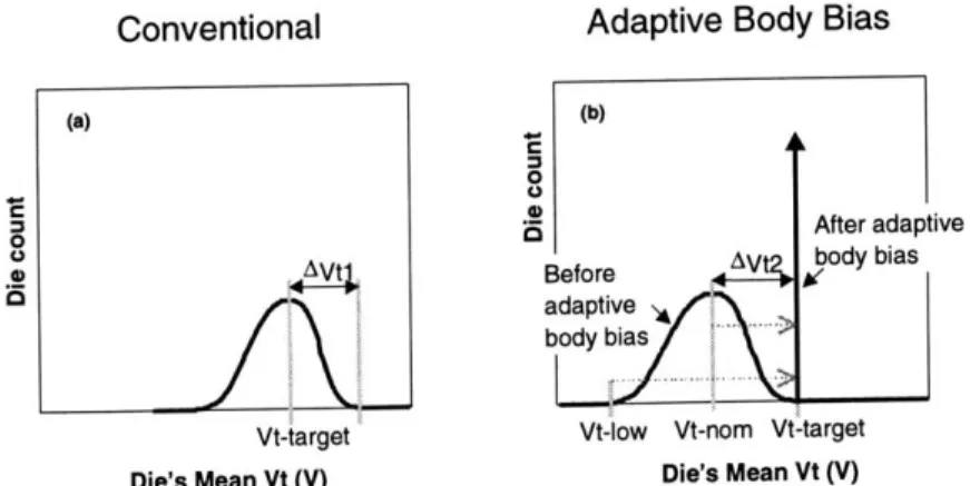
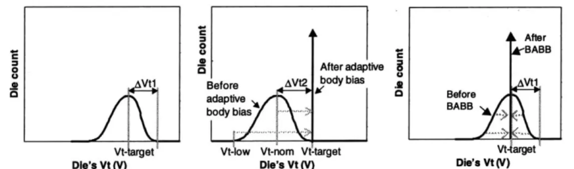
Supply voltage (Vdd) and threshold voltage (Vt) scaling is the most effective approach to keep active power dissipation under control while maintaining performance improvement [9]. One of the limits to Vdd scaling is the expected increase in Vt variation [8, 13]. Increase in die-to-die Vt variation will result in slow dies that do not meet the frequency target and fast dies that exceed the allowed power limits due to excessive leakage. The resulting reduction in yield will lead to increases in manufacturing cost and time to market, neither of which is acceptable especially with the technology life cycle shrinking from 3.6 to 2 years (Figure 1-1). Adaptive body bias schemes have been proposed in the past to reduce this expected increase in die-to-die Vt variation [20, 21].
Conventional Adaptive Body Bias
(a) (b)
0
0 After adaptive
AvtrBoe body bias
adaptive body bias
Vt-target Vt-low Vt-nom Vt-target
Die's Mean Vt (V) Die's Mean Vt (V)
Figure 3-1: Die-to-die threshold voltage distributions (a) Conventional approach without adaptive body bias
(b) Adaptive body bias approach.
Figure 3-1(a) illustrates that in a conventional approach without adaptive body bias the mean Vt of
all the die samples do not match the target Vt. By using adaptive body bias, a sharper distribution in die-to-die Vt variation can be achieved, as shown in Figure 3-1(b). Adaptive body bias first requires modification of the process so that mean Vt of all the dies are lower than the target Vt, as depicted in Figure 3-1(b). This lowering of Vt for a given technology is accomplished by reducing the channel doping which increases the depletion width of the MOSFET parasitic junction diodes. It was shown in Section 2.1 that this would result in increased Vt variation due to worsened short channel effect (SCE)! Therefore, AVt2 > AVt1 in Figure 3-1. After this process modification, depending on the mean Vt of a die sample an adaptive amount of reverse body bias is applied to the entire die so that its mean Vt will be increased to match the target Vt, as illustrated in Figure 3-1(b).
Reverse body bias increases the depletion width of the MOSFET parasitic junction diodes [29]. It was shown in Section 2.1 that this would result in increased Vt variation due to worsened short channel effect (SCE)! The research objectives in Section 3.1 are (1) to study the effectiveness of adaptive body bias in controlling die-to-die Vt variation as technology is scaled and (2) to determine impact of adaptive body bias on within-die Vt variation. It will shown that as MOSFET technology is scaled, the body bias required for compensating die-to-die Vt variation increases, which in turn further increases SCE, and, because of this increase in SCE, within-die Vt variation becomes worse. It will also be shown that the die that requires larger body bias to match its mean
Vt to the target Vt will end up with a higher within-die Vt variation. The resulting increase in within-die Vt variation due to adaptive body bias can impact clock skew, worst-case gate delay, worst-case device leakage current, total chip leakage power, and analog circuit performance. More importantly, increase in within-die Vt can also reduce the frequency of operation in high performance designs that have increasingly lesser logic stages between flip-flops [32, 34]. This will be elaborated in the second of this chapter. In the rest of this section, the effectiveness of adaptive body bias and within-die Vt variation due to adaptive body bias will be analytically quantified for three technology generations. To reiterate the point from Section 2.1, the focus of Vt variation in this thesis is due to worsening SCE with technology scaling and channel length variation.
3.1.1 Adaptive body bias and short channel effect (SCE)
For adaptive body bias the Vt of the process technology has to be re-targeted to be lower as shown in Figure 3-1. In a given technology this is achieved by lower channel doping that will result in lower body effect to begin with. Since adaptive body bias depends on body effect to modulate Vt
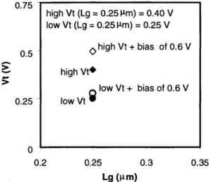
with reverse body bias, lowering Vt will render adaptive body bias less effective. The body effect is further reduced in short channel devices because lower Vt with reduced channel doping will increase diode depletion charge and SCE. Figure 3-2 illustrates the reduction in body effect due to
Vt lowering in a 0.25 gm technology. For an MOS device with Vt of 0.4 V, reverse body bias of 0.6
V increased the Vt by 25%. Vt modulation for the same amount of reverse body bias reduces to less than 8% for an MOS device with Vt of 0.25 V.
0.75
high Vt (Lg = 0.25 9m) = 0.40 V low Vt (Lg = 0.25 9m) = 0.25 V 0.5 -high Vt +bias of 0.6 V
high Vt*
0.25 low Vt low Vt + bias of 0.6 V
0
0.2 0.25 0.3 0.35
Lg (9pm)
Figure 3-2: Reduction in Vt modulation with reverse body bias with reduction in Vt.
high Vt + ias of 0.6 V low Vt + bias of C.6 V hig lt low Vt 0.2 0.25 0.3 0.35 Lg (Pm)
in Vt-roll-off with Vt reduction and reverse body bias increase.
Furthermore, since Vt reduction degrades short channel effect, Vt-roll-off with channel length
35 U.70 I 0.5 -0.25 0 Figure 3-3: Increase
reduction should be more for the lower-Vt device. In addition, reverse body bias will further increase the Vt-roll-off as shown in Figure 3-3.
It is known that increase in reverse body bias worsens MOSFET's short channel effect. Figure 3-4 shows sub-threshold characteristics of a 0.25 pm NMOS device. Using Drain Induced Barrier Lowering (DIBL) which is AVt observed for a given AVds, as another figure of merit to indicate short channel effect, we see that increasing reverse body bias (Vsb) from 0 V to 2 V increases AVt and hence DIBL, by 88%.
1e-3 Vds=1V 1e-5 A Vt1 40 mV
E
Vds= 50 mV Vsb = 2 V 1e -7 - - - - --- Vsb= 0 V1e-9
AVt2=75
mV 1e-11 0 0.5 1 1.5Vgs (V)
Figure 3-4: Increase in DIBL due to increase in reverse body bias.
3.1.2 Scaling of required body bias and SCE increase
Increase in Vt-roll-off due to adaptive body bias will lead in increase in within-die Vt variation. To quantify the impact of adaptive body bias on within-die Vt variation, we first determine the bias required to reduce die-to-die Vt variation, for two scaling scenarios, starting from a 0.25 gm technology as shown in Table 1. Once we determine bias required to reduce die-to-die Vt variation, we then determine, the SCE increase indicated by Drain Induced Barrier Lowering (DIBL) and the resulting increase in within-die Vt variation.
In Table 3-1, Lg, Tox, Xj, Vdd, and Vt-linear are gate length, oxide thickness, junction depth, supply voltage, and linear threshold voltage respectively. In both scaling scenarios Lg, Tox, Xj, and
Vdd scale by 30%. While Vt-linear scales by an aggressive 30% in the first scenario, it scales by a
less aggressive 20% in the second. Equation (1) gives threshold voltage for a short channel NMOS by including body effect reduction factor, )b, from [30] and DIBL, Ad [31]. Using (1) with Vsb = 0 and Vds -+ 0, we can determine the channel doping N, for a given Vt-linear. The calculated values of N for the target devices are also listed in Table 3-1.
I..Q25...
0.8.5...0
35.j
0.5
Q .2.
400e-
280e-35.99E+1 7
7,37E+1 70.13 25 [0.025 1.2 196e-3 9.26E+17
20% Vt scalin
Tabl 5x Acnlg me unde twoscan s
0.18 3 0,5 1.8 320e-3 8,2+1 7
0.3 25 0.025 1.2 256e-3 1.21 E+1 8
Table 3-1: Technology parameters under two scaling scenarios.
With channel doping known, we can determine DIBL, Ad, using equation (2), which has been verified for accuracy down to Lg = 0.1 gm [31]. It is important to note that equation (2) is empirical and therefore its form cannot be explained using physical reasoning. With Ad and
Vt-linear known, we can now estimate Vt-target, the saturation threshold voltage for the target device.
*0 0 0 CD 0) U Die-to-die variation (a) A Before adaptive body bias '..9 .... After adaptive body bias A"
Vt-low Vt-nom Vt-target
Die's Mean Vt (V)
Within-die variation
(b)
Die 1
Die 2 Die 1 + bias
Die 2 + bias
Vt-low Vt-nom Vf-target Within-die Device Vt (V)
Figure 3-5: (a) Adaptive body bias reduces the die-to-die Vt variation. (b) Within-die Vt variation increases for die samples that require body bias to match their mean Vt to the target Vt. Vt-target is the target saturation threshold voltage for a given technology. Vt-low and Vt-nom are the minimum and mean threshold voltages of the die-to-die distribution.
V =VJ +1 20s+p2qN, , |+V )-AV, ; W = 26
s(I2
I+VbqN
'd -DIBL ) L=Lg 2Xj -- 2.7L
2.2/m
(T+
0.012/tm) (Wsd +0.15/tm) (X
1+
2.9/tm)
1(2)
26s
2Es
(W +W );W, = (Obi +Vb) ;Wd =q
+V, +Vsb )qN
qN
AV
Dd~d +
Vt
dl
f
+Vd
from
(1)
AL
AsdL
a2bd L
__ AL_> (3).. AV =2.7 Vdd Ad+ 2qNe,(|2p|+Vsb) (1-A)
C,
aoxassume
VdS= VddJ 39Y(1)
'd Wsd1w
(F
-- l -: j;
xj
L
Let us now define Vt-nom and Vt-low to be the mean saturation threshold voltages of two different die samples as shown in Figure 3-5(b). Vt-nom is also the mean saturation threshold voltage of the die-to-die distribution as shown in Figure 3-5(a), and is due to 2.5% reduction in Lg,
Tox, and N, and 2.5% increase in Xj, from the target device. Similarly, Vt-min is the minimum
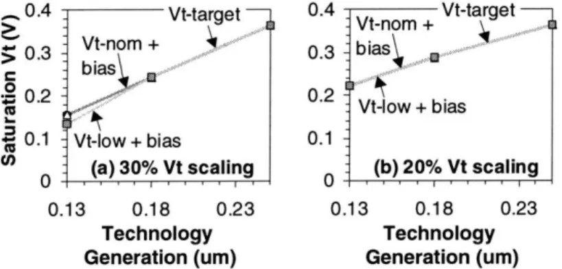
saturation threshold voltage of the die-to-die distribution, and is due to 5% change in Lg, Tox, N, and Xj from the target device. The values of Vt-target, Vt-nom, and Vt-min, before adaptive body bias are illustrated in Figure 3-6. Using equation (1) we can determine the body bias required to increase the saturation threshold voltage of the Vt-nom and Vt-min devices to Vt-target. The resulting saturation threshold voltages after adaptive body bias are depicted in Figure 3-7. The required bias values to match the saturation threshold voltages under the two scaling scenarios are given in Table 3-2 within parenthesis.
0.4 - 0.4 - Vt-target Vt-target :Vt-nom V 0.3 Vt-nom , 0.3 > 0.2 - -n 0.2 Vt-low .20.2 Vt-lowO 0.1 0.1
C (a) 30% Vt scaling (b) 20% Vt scaling
0 1.1 I I . 0 . .I . . . . I I .
0.13 0.18 0.23 0.13 0.18 0.23
Technology Technology
Generation (um) Generation (um)
Figure 3-6: Trend in mean saturation threshold voltage of different die samples before adaptive body bias under (a) 30% Vt scaling and (b) 20% Vt scaling scenarios.
0.4 Vt-target 0.4 Vt-target -Vt-nm +Vt-nom + -5 0.3 Vt-nom + 0.3 bias bias 0.2 0.2 cc Vt-low + bias 0.1 Vt-low + bias 0.1
(a) 30% Vt scaling (b) 20% Vt scaling
0 - . 0- .
0.13 0.18 0.23 0.13 0.18 0.23
Technology Technology
Generation (urn) Generation (um)
Figure 3-7: Matching of mean saturation threshold voltages of different die samples with adaptive body bias under (a) 30% Vt scaling and (b) 20% Vt scaling scenarios.
Comparing Figure 3-6 and Figure 3-7, it is clear that adaptive body bias will reduce die-to-die
Vt variation. It is also clear from Table 3-2 that the bias required to match die-to-die Vt variation
increases with scaling. Note from Figure 3-7 (a) that under 30% Vt scaling, adaptive body bias was unable to increase Vt-low (103 mV) to Vt-target (156 mV) for 0.13 gm technology due to body effect reduction with bias [30]. For body bias above 1.34 V the saturation threshold voltage of this
device saturates at 134 mV.
DIBL increase and body effect factor reduction for the different devices with and without body bias can be estimated using equation (2), and the values are listed in Table 3-2. As expected, SCE (DIBL increase and body effect reduction) becomes worse with scaling and degrades further with body bias. In addition, the increase in SCE due to adaptive body bias escalates with technology scaling, since the amount of bias required for reducing die-to-die Vt variation increases.
0.18 0.74, 21 0.13 0.70, 32 20% Vt scalinq U.7b, If 0.72.,24
-I
-I I-0.68, 38 0.69, 27 (0.31) 0.62, 44 (0.49)'I
U.(/4, zU 0.70, 29 0.65,44-I-0.59, 40 (1.13) 0.52, 64 (1.34) 0.25 0.78, 15 0.76, 17 0.74,18 (0.24) 0.74, 20 0.68, 25 (0.66) 0.18 0.75,19 0.73,23 0.71, 25 0.28 0.71, 27 0.63, 34(0.84) 0.13 0.73, 28 0.71, 33 0.67, 36 (0.34) 0.68, 39 0.57, 53 (1.26) Table 3-2: With adaptive body bias short channel effect of devices increase, indicated by DIBL (lid in mVN) increase and body effect reduction factor (4) decrease. This SCE increase is worse for Vt-low devices, compared to Vt-nom devices, as they require larger body bias to match Vt-target. The required bias values (in V) are indicated within parentheses.
3.1.3 Impact on within-die threshold voltage variation
If for a given technology within-die Vt variation is primarily due to variation in critical dimension, equation (3) shows that within-die Vt variation of a device depends on its DIBL (Ad) and body effect reduction factor (Ad). Hence, the increase in DIBL and decrease in body effect with
41
I
I
_
_
adaptive bias will be translated to increase in within-die Vt variation. In other words, the within-die
Vt variation of a die sample whose mean saturation threshold voltage was made to align with Vt-target using body bias, will be worse than that of the die sample whose mean saturation voltage
was Vt-target to begin with.
For example, for the 0.25 gm technology with 5% (12.5 nm) variation in within-die Lg, the die sample whose mean saturation threshold voltage was Vt-target to begin with, is estimated to have a within-die Vt variation of 8.2 mV. On the other hand, after adaptive body bias, the within-die Vt variation for the die sample with Vt-low (Vt-nom) as the mean threshold voltage is estimated to be 15.7 mV (11 mV). So, the saturation threshold voltage ranges for the Vt-target, Vt-nom, and Vt-low die samples will be 363 mV ± 8.2 mV, 363 mV ± 11 mV, and 363 mV ± 15.7 mV respectively.
If we assume that within-die variation in critical dimension is 5% of target Lg then the percentage variation in Vt can be calculated using equation (3) and is illustrated in Figure 3-8. Clearly, with scaling within-die Vt variation due to adaptive body bias increases and is more pronounced for aggressive Vt scaling. This increase in within-die Vt variation can impact clock skew, worst-case gate delay, worst-case device leakage current, total chip leakage power, and analog circuit performance.
40% 30%Vt scaling 40% 20%Vt scaling
'M 30% Vt-low + bias 30% Vt-low + bias Vt-nom + bias N. Vt-nomn + bias 20% Vt-target 20% 10% 10% 0% 0% 1 0.13 0.18 0.23 0.13 0.18 0.23 Technology Technology
Generation (urn) Generation (um)
Figure 3-8: Increase in within-die threshold voltage variation due to increase in short channel effect with adaptive body bias under (a) 30% Vt scaling and (b) 20% Vt scaling. We assume that the dominant reason for within-die Vt variation is critical dimension variation. The results shown here assume within-die variation in
Lg of 5%.
3.1.4 Summary
We showed that although adaptive body bias reduces die-to-die Vt variation it increases within-die Vt variation, due to increase in short channel effect. Moreover, we quantified this increase under two Vt scaling scenarios. The analysis showed that the increase in within-die Vt variation due to adaptive bias worsens with scaling and is more pronounced for aggressive Vt scaling. Consequently, to make effective use of the traditional adaptive body bias scheme one should consider (a) the maximum acceptable within-die Vt variation increase that can be tolerated for a given design and (b) the use of multiple adaptive bias generators within-die on a triple well process. Even if these techniques are employed to minimize impact of adaptive body bias on with-die Vt variation, adaptive body bias is still destined to become less effective with scaling due to increased SCE and weakening body effect. In addition, circuits that cannot tolerate increase in short channel effect due to reverse body bias should be isolated not to receive body bias. This will require triple-well process if adaptive body bias needs to applied for both PMOS and NMOS devices.
In the next section, a scheme called bi-directional adaptive body bias is introduced. This scheme does not require process modification for Vt re-targeting, minimizes die-to-die Vt variation without impacting Vt within-die variation, and more importantly, its effectiveness scales better with technology compared to the traditional adaptive body bias. The bi-directional adaptive body bias scheme discussed in the next section is designed to minimize the variation in microprocessor operating frequency due to within-die and die-to-die Vt variations. The testchip was designed in collaboration with James Kao (MIT Ph.D. 2001). My contributions were to (i) study the impact that within-die variation plays on the microprocessor frequency distribution and (ii) determine the proper bias circuit impedance required to ensure minimal impact of noise on the stability of the bias value. The details of the testchip and measurement results are discussed in Section 3.2 and the bias circuit impedance requirement and measurement results are discussed in Section 3.3.
3.2 Bi-directional adaptive body bias
Both die-to-die and within-die Vt variations, which are becoming worse with technology scaling, impact clock frequency and leakage power distributions of microprocessors in volume manufacturing [32]. In particular, they limit the percentage of processors that satisfy both minimum frequency requirement and maximum active switching and leakage power constraints. Their