HAL Id: hal-00189476
https://hal.archives-ouvertes.fr/hal-00189476
Submitted on 21 Nov 2007HAL is a multi-disciplinary open access
archive for the deposit and dissemination of sci-entific research documents, whether they are pub-lished or not. The documents may come from teaching and research institutions in France or
L’archive ouverte pluridisciplinaire HAL, est destinée au dépôt et à la diffusion de documents scientifiques de niveau recherche, publiés ou non, émanant des établissements d’enseignement et de recherche français ou étrangers, des laboratoires
A SCANNING FLUORESCENT PROBE FOR LOCAL
TEMPERATURE IMAGING OF
MICROELECTRONIC CIRCUITS
L. Aigouy, G. Tessier, M. Mortier, B. Charlot
To cite this version:
L. Aigouy, G. Tessier, M. Mortier, B. Charlot. A SCANNING FLUORESCENT PROBE FOR LOCAL TEMPERATURE IMAGING OF MICROELECTRONIC CIRCUITS. THERMINIC 2005, Sep 2005, Belgirate, Lago Maggiore, Italy. pp.220-223. �hal-00189476�
A SCANNING FLUORESCENT PROBE FOR LOCAL TEMPERATURE IMAGING
OF MICROELECTRONIC CIRCUITS
L. Aigouy
1, G. Tessier
1, M. Mortier
2and B. Charlot
31
Laboratoire ‘Spectroscopie en Lumière Polarisée’, UPR A0005 du CNRS, ESPCI,
10 rue Vauquelin, 75231 Paris Cedex 5, France
2
Laboratoire de Chimie Appliquée de l'Etat Solide, UMR 7574 du CNRS, ENSCP,
11 rue Pierre et Marie Curie, 75231 Paris Cedex 5, France
3
TIMA, 46 Avenue Félix Viallet, 38031 Grenoble, France
ABSTRACT
A fluorescent particle settled at the extremity of an atomic force microscope tip is used as a scanning temperature sensor. Since fluorescence is an effect that depends on temperature, by collecting the amount on light emitted by the particle as a function of its position on a sample, we are able to map the heat distribution on its surface. To validate the technique, we have imaged the heating of a stripe resistor.
1. INTRODUCTION
An important and useful application of scanning probe microscopy concerns the study of thermal effects on inhomogeneous materials or microelectronic circuits [1]. These effects are for example linked to the determination of intrinsic physical parameters of materials such as their thermal conductivity [2] or to the mapping of the thermal conductivity on phase-separated compounds and artificial structures [3,4]. Another technological issue is related to the visualization of hot zones in operating microelectronic circuits [5]. The visualization of hot zones is an important application since it can allow to determine the position of possible defects and weak points as well as to find out how heat can be dissipated in the circuits.
Until now, scanning thermal probes have mainly used two main types of sensors located at the extremity of atomic force microscope (AFM) tips: a thermocouple or a resistive wire. Thermocouple-based probes are fabricated by several technological steps in clean rooms [5]. Two metallic stripes are generally evaporated and connected at the end of the tip to form a thermocouple junction. They allow the determination of the local temperature of a sample with a submicron lateral resolution [6]. Resistive probes [4,7] are formed by a metallic wire (a platinum rhodium alloy for example) that forms the tip of the AFM. Its section is reduced to the micrometer range to
allow the measurement of topographies as well as thermal effects. The temperature variations and heat transfers between the tip and the sample surface are determined by monitoring the variations of the filament resistance. Such a probe has also demonstrated a lateral resolution much smaller than the micrometer [1,4].
Recently, a technique that employs a layer of europium-based fluorescent dyes spin-coated on a microheater has been developed to monitor temperature variations of the device [8]. The fluorescent dyes, spread all over the circuit, emit less light on hot zones than on cold ones allowing to map the temperature distribution on the sample.
In this communication, we will present a technique based on a similar effect, but that employs a single fluorescent particle as a temperature sensor. In our case, the fluorescent fragment is settled at the extremity of an AFM tip and behaves like a scanning thermal probe. By monitoring the fluorescence intensity variations of the particle as a function of its position on the surface of a microelectronic circuit, we are able to determine the absolute temperature of the particle and therefore of the zone of the device it is in contact with.
2. THE TEMPERATURE DETERMINATION PROCESS
The fluorescent particles are glass ceramic fragments that contain erbium and ytterbium ions [9]. A scanning electron micrograph of such a particle settled at the extremity of an AFM tip is given on Fig. 1. The particle is glued at the tip end using nanomanipulators [10] with a temperature resistant, UV curable, polymer glue. The particle is excited using a 980 nm laser diode (by a 2-photon absorption process). It emits light at different wavelengths: in the visible, fluorescence occurs at 520nm, 550nm and 670nm.
The excited energy levels (2H
11/2 and 4S3/2) involving
the 520nm and 550nm lines have the peculiarity of being in thermal equilibrium. This means that the relative
L. Aigouy, G. Tessier, M. Mortier and B. Charlot
A SCANNING FLUORESCENT PROBE FOR LOCAL TEMPERATURE IMAGING ...
Fig. 1 : Scanning electron micrograph of a fluorescent particle glued at the end of an AFM tip.
population of the two levels depends on temperature. The relative area of the two fluorescence peaks are therefore linked by an exponential law that directly depends on temperature [11] : β α+ − ≅ ⎟⎟ ⎠ ⎞ ⎜⎜ ⎝ ⎛ T I I 1 2 ln (1)
where I2 and I1 are the area of the peaks located at 520nm
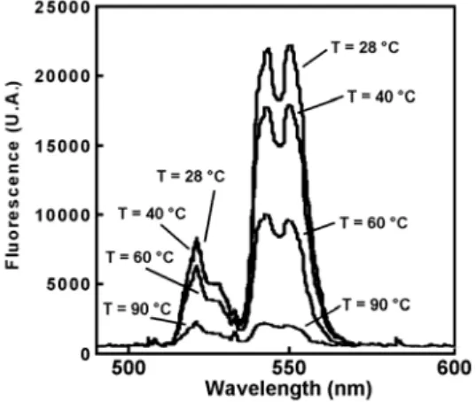
and 550nm, α and β are coefficients and T is the temperature. When temperature increases, the peak located at 550nm diminishes more rapidly than the one located at 520nm (see Fig. 2). Therefore, it is possible to determine the temperature of the particle by measuring the amount of fluorescence emitted at 520nm and 550nm. Since the particle is in contact with a sample during a scan, its temperature reflects the temperature of its surface.
The calibration of the coefficients α and β is performed by measuring the fluorescence spectrum of a micron-sized particle deposited on a substrate heated at a known temperature. The thermal conductivity of the particle is 0.8 W.m-1.K-1.
3. THE EXPERIMENTAL SET-UP
The experimental setup is a homemade AFM combined with an optical microscope able to detect the fluorescence emitted by the particle with a high sensitivity. It is sketched on Fig. 3. A 980nm laser diode is focused on the tip extremity and the sample surface. The diode is internally modulated at around 620Hz. Two different interferential filters are placed in front of two photomultiplier tubes (PMT): one is centered at 520nm and the other one at 550nm. The bandwidth of these filters is 10nm. The fluorescence of the peaks can then be measured independently and simultaneously when the tip is scanned on the surface. The fluorescence of the fragment is collected with a high numerical aperture objective followed by a beam splitter that sends the
emitted photons towards the two PMTs. Afterwards, the signals are detected by two lock-in amplifiers synchronized to the laser diode modulation frequency and are sent to a computer for recording and processing.
Fig. 2 : Dependence of the particle fluorescence as a function of temperature.
The tip is scanned in intermittent contact on the sample surface, in the tapping mode. Its oscillation frequency is around 5kHz (around ten times higher than the fluorescence modulation frequency) and its amplitude is around 10nm.
In order to validate our experimental technique, an operating microelectronic circuit seemed to be a good candidate. Three images are acquired. The first one is the topography of the chip. The second and the third ones are the fluorescence images at the two different wavelengths. As it can be seen in eq. (1), the ratio of the two fluorescence images permits to determine if some zones are hotter than others.
4. VISUALIZING THE HEATING OF AN OPERATING MICROELECTRONIC CIRCUIT The microelectronic circuit we have tested is a polysilicon resistor stripe implemented on a standard 0.8µm CMOS process. The stripe has a width of 20µm and a height of approximately 600nm. The experiment has been performed at two different DC voltages. The current flowing in the device is therefore constant. We first describe the experimental procedure used to visualize the temperature heating. Afterwards, we will present the experimental results and discuss on the uncertainties and the different factors that can influence the measurements. 4.1. Description of the experimental procedure
First, measurements have been achieved when no current is flowing through the resistor. This allows to have a reference for the optical contrast at room temperature. We can expect that two zones made of a different material (for instance, the resistor and the substrate) will have a different optical image at the two wavelengths. Indeed, the reflection coefficient of both the exciting laser beam and the fluorescence lines will not be the same on the resistor and on the substrate. Therefore, even if the temperature of the whole system is the same, the ratio of the two fluorescence images will be different on different materials.
For the second scan, a DC voltage of 25V is applied to the stripe generating a constant current of around 50mA. Under this high current, the stripe is heating and the heat is spreading all around the substrate.
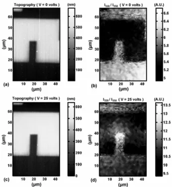
The ratio of the two fluorescence images and its comparison with the reference one at room temperature allows to see if the sample has heated and where. The results are shown on Fig.4.
4.2. Experimental results
The optical image (b) corresponds to the ratio of the fluorescence signals of the particle (I520 / I550) when no current is flowing. The temperature is the same everywhere. Since the polysilicon resistor and the silicon substrate have different optical properties, they appear contrasted on this image. The resistor appears darker than the substrate. The values of the scale bar indicated on the right are arbitrary units.
The optical image (d) corresponds to the same ratio but a current of around 50mA is flowing through the resistor (V=25volts). The stripe is still clearly visible but some features have appeared. First, on the stripe, a gray, curved zone is visible. It corresponds to a hot zone through which the majority of the electrons are probably passing. Second, in the middle, a bright zone is also
dominating the image. This area corresponds to a hot zone of the substrate which is created by heat diffusion from the elbow of the stripe nearby.
Fig. 4: (a) Topography of the stripe and (b) ratio of the two fluorescence images (I520 / I550) when no current is flowing through the resistor ; (c) topography of the stripe and (d) ratio of the two fluorescence images when a voltage of about 25V is applied. The fluorescence images have been treated using a 3x3 median filter to eliminate noise.
Note that, if we look at the scale bar of Fig 4d, the values are much higher than in the image obtained at room temperature (Fig. 4b), indicating that the whole scanned area has heated. A rough estimation, not detailed here, indicates that the temperature is approximately equal to 70°C on the lower part of the substrate and 90°C in its hot area of the middle. On the stripe, the temperature also varies from around 80°C in the ‘cold’ zone to 100°C in the hot one. The time necessary to perform a thermal image is around half an hour.
4.3. Discussion
The first point we would like to discuss is the influence of the tip on the measurement. Does the tip modify the real temperature of the device? As can be seen on Fig. 1, the size of the particle is smaller than one micrometer and the tip that holds it is very sharp. The point of contact with the surface is therefore very small. Besides, it is intermittent since the tip is oscillating on the surface in the tapping mode. We do not think that the tip perturbs enormously the temperature and the operation of the device, at least no more than most other scanning
probe microscope tips that have a spatial extension much larger above the surface.
The other question we can ask is linked to the signal measured by the tip. How close is it to the real temperature of the surface? Indeed, since the tip is in intermittent contact with the sample, the heat transfer mechanisms are complicated. The oscillation amplitude of the tip is around 10nm. During its movement, the time the tip remains in direct contact with the surface depends on the offset used for the feedback mechanism. By varying this parameter and by changing the oscillation amplitude, we do not have observed a noticeable variation of the signals. Besides, almost no significant difference could be observed when the tip was in contact with the surface and when it was situated at several hundreds of nanometers from it. This shows that the heat transfer mechanism in air was important in this experiment. This is not surprising since the size of the device is significantly larger than the tip itself. A different behavior would probably be observed on submicron devices or structures like carbon nanotubes for which air heating is much smaller due to their reduced spatial extension.
Regarding the spatial resolution of the measurements, we can expect it to be of the same order as the particle size in the best case. In principle, a 100nm resolution could be obtained for a 100nm sized particle. Since the tip is very sharp, indirect heating from its far zones and from the cantilever is small. For the device we have studied, it is not possible to determine the real lateral resolution of the method since the heat is diffusing over distances much larger than the particle size. Experiments carried out on smaller circuits will soon be performed.
5. CONCLUSION
The technique we have developed allows to visualize the hot zones of operating microelectronic circuits. It is based on the measurement of the fluorescence of a submicron-sized particle settled at the extremity of an AFM tip. The method permits the determination of the absolute temperature of the device. We are currently performing experiments to determine the limits of the technique in terms of lateral resolution and sensitivity. In particular, we are studying well-defined resistor with integrated diodes which allow the precise temperature calibration of the technique.
6. ACKNOWLEDGMENTS
The authors strongly thank D. Fournier for stimulating and motivating discussions.
7. REFERENCES
[1] H.M. Pollock, and A. Hammiche, “Micro-thermal analysis: techniques and applications,” J. Phys. D : Appl. Phys. 34, Institute of Physics Publishing, UK, pp. 23-53 (2001).
[2] F. Ruiz, W.D. Sun, and F.H. Pollak, “Determination of the thermal conductivity of diamond-like nanocomposite films using a scanning thermal microscope,” Appl. Phys. Lett. 73(13), American Institute of Physics, USA, pp. 1802-1804 (1998). [3] V.V. Gorbunov, N. Fuchigami, J.L. Hazel, and V.V. Tsukruk, “Probing surface microthermal properties by scanning thermal microscopy,” Langmuir 15(24), American Chemical Society, USA, pp. 8340-8343 (1999).
[4] S. Lefèvre, and S. Volz, “3ω-scanning thermal microscope,” Rev. Sci. Instrum. 76, American Institute of Physics, USA, pp. 033701-1-6 (2005).
[5] G. Mills, H. Zhou, A. Midha, L. Donaldson, and J.M.R. Weaver, “Scanning thermal microscopy using batch fabricated thermocouple probes,” Appl. Phys. Lett. 72(22), American Institute of Physics, USA, pp. 2900-2902 (1998).
[6] L. Shi, S. Plyasunov, A. Bachtold, P.L. McEuen, and A. Majumdar, “Scanning thermal microscopy of carbon nanotubes using batch-fabricated probes,” Appl. Phys. Lett. 77(26), American Institute of Physics, USA, pp. 4295-4297 (2000). [7] P.G. Royall, V.L. Kett, C.S. Andrews, and D.Q.M. Gray, “Identification of crystalline and amorphous regions in low molecular weight materials using microthermal analysis,” J. Chem. Phys. B 105, American Chemical Society, USA, pp. 7021-7026 (2001).
[8] E. Van Keuren, M. Cheng, O. Albertini, C. Luo, J. Currie, and M. Paranjape, “Temperature profiles of microheaters using fluorescence microthermal imaging,” Sensors & Materials
17(1), MYU Tokyo, Japan, pp. 1-6 (2005).
[9] L. Aigouy, Y. De Wilde, and M. Mortier, “Local optical imaging of nanoholes using a single fluorescent rare-earth-doped glass particle as a probe,” Appl. Phys. Lett. 83(1), American Institute of Physics, USA, pp. 147-149 (2003). [10] L. Aigouy, Y. De Wilde, M. Mortier, J. Giérak, and E. Bourhis, “Fabrication and characterization of fluorescent rare-earth-doped glass-particle-based tips for near-field optical imaging applications,” Appl. Opt. 43(19), Optical Society of America, USA, pp. 3829-3837 (2004).
[11] M.A.R.C. Alencar, G.S. Maciel, C.C.B. de Araujo, and A. Patra, “Er3+-doped BaTiO
3 nanocrystals for thermometry:
influence of nanoenvironment on the sensitivity of a fluorescence-based temperature sensor,” Appl. Phys. Lett.
84(23), American Institute of Physics, USA, pp. 4753-4755
(2004).