DESIGN AND FABRICATION OF A VERTICAL POWER MOSFET WITH AN INTEGRAL TURN-OFF DRIVER
by
JOSEPH BARRY BERNSTEIN
B.S. IN ELECTRICAL ENGINEERING, UNION COLLEGE (1984)
SUBMIITED IN PARTIAL FULFILLMENT OF THE REQUIREMENTS FOR THE DEGREE OF MASTER OF SCIENCE
IN ELECTRICAL ENGINEERING AND COMPUTER SCIENCE
at the
MASSACHUSETTS INSTITUTE OF TECHNOLOGY Sept 1986
@ Massachusetts Institute of Technology
1986
Signature of Author
DepS reref' of Ele6trical Engineifg and Computer Science
August 8, 1986
Certified By->
Martin F. Schlecht
,Thesis Supervisor
Accepted By
-SAtnhur
C. Smithl
Chairman, Departmental Committee on Graduate Studies
ARCHIVES
MASSACHUSETTS INS•TITUTE
OF TECHNGOLGGY
JAN 2 7 1987
Design and Fabrication of a Vertical Power MOSFET with an
Integral Turn-OFF Driver.
by
Joseph Barry Bernstein
Submitted on August 8, 1986,87 in partial fulfillment of the requirements for the degree of Masters of Science in Electrical Engineering at the Massachusetts Institute of Technology.
ABSTRACT
The circuitry which delivers power to a computer system has not experienced the extensive miniaturization of the rest of the computer over the past decade. To reduce the size and cost of power delivery systems, the technology is being developed at MIT for increasing the operating frequency of switching converters. However, in order to achieve a significant increase in the switching frequency, the per-cycle energy dissipation in the power MOSFET must be diminished.
Losses in a power MOSFET generally result from the inability of the gate drive to adequately control the gate voltage of the switch. Parasitic capacitances interact with the resistance and inductance of a physically separate driver, resulting in a miller effect which tends to delay the turn-off and cause dissipation in the device. This effect can be minimized by reducing the capacitance associated with a vertical DMOS and eliminating the inductance associated with the gate drive.
A process has been developed, along with the necessary masks, for fabricating a vertical power DMOS with reduced capacitance for a given on-state resistance. It also contains a low voltage planar MOSFET integrated on the structure to serve as the gate driver during turn-off. The combined structure nearly eliminates the power dissipation due to the miller effect by providing a low resistance path from the gate to the source, increasing the speed of the turn-off, and reducing the power lost by nearly a factor of 5.
Thesis Supervisor
:
Martin
F. Schlecht
ACKNOWLEDGMENTS
This project could not have been completed without the constant guidance and assistance of my advisor, Martin Schlecht, who coached me along when I needed it, but gave me ample freedom to learn and create on my own. As for the fabrication of the devices, I am grateful to all the students and staff in the Microelectronics Laboratory at MIT who helped me master the skills required to design, lay out, and produce the devices. Particularly, I wish to thank Gary Ditmer and Lawrence Bair for having such patience with me. Furthermore, my fondest wishes go to my office mate, Khalid Rhamat, who was always there to offer a sympathetic ear. I especially wish to express my appreciation to my family and friends for their moral support and companionship whenever I needed it, and to the MIT Folk Dance club for providing a consistent source of socialization and recreation.
Abstract 2
Acknowledgments 3
Contents 4
List of Figures 5
Chapter 1. Introduction 6
1.1 Increasing power density 7
1.2 Improving the semiconductor devices 9
Chapter 2. Justification 14
2.1 Quasi-resonant approach 15
2.2 Turn-off limitations 17
2.3 Integrating a turn-off driver 21
Chapter 3. Design details 24
3.1 Decreasing the on-state resistance 31 3.2 Integrating the turn-off driver 35 3.3 Calculated properties of the design 41
Chapter 4. The Fabrication Process 46
4.1 Gate oxide and polysilicon 48
4.2 Double diffusion 49
4.3 P+ source contact 51
4.4 Polysilicon etch 52
4.5 Isolation oxide etch 53
Chapter 5. Mask Details 56
5.1 Oversized flashes 57
5.2 Alignment markers 60
5.3 Individual mask layers 62
Chapter 6. Results 67
6.1 Tested devices
6.1.1 Vertical Power DMOS 67
6.1.2 Lateral Driver 70
Chapter 7. Conclusions and Recommendations 72
7.1 What's next 73
References 76
5
LIST OF FIGURES
1-1 Schematic representation of a distributed power delivery system 6 1-2 Simplified cross-section of a single DMOS cell 10 1-3 Power MOSFET with an integrated shorting switch 11 2-1 I and V waveforms for a generalized switch in a power circuit 14 2-2 Schematic of the circuit topology used for high frequency switching 15 2-3 Schematic of the DMOS and associated parasitic elements 18 2-4 waveforms of the turn-off of a standard DMOS 19 2-5 More complete parasitic representaion of the DMOS 20 2-6 Modified DMOS structure with an integrated turn-off driver 21 2-7 Predicted waveforms of the modified device during turn-off 23
3-1 Cross section of a Vertical DMOS 24
3-2 Some typical dimensions for a 200V vertical power DMOS 25
3-3 Detail of the first mask layer 26
3-4 Cross section showing current flow path 28
3-5 Cross section of an OFF device 29
3-6 Top view and cross section of p-type guard rings 30 3-7 Cross sections showing double self-aligned process 32 3-8 Double diffusion and guard ring placement with first mask 33 3-9 Matrix of devices used for determining the optimal geometry 35
3-10 Cross section of the integrated driver 36
3-11 Basic scheme for incorporating the driver around the DMOS 39 3-12 Detail of a single device showing the interdigitated metalization 40 3-13 Metaliztaion detail in the center of the device 41 3-14 Cross section of the vertical DMOS showing the parasitic elements 43 3-15 Cross section showing the final metalization and the driver 45 4-1 Cross section of the wafer with gate oxide and polysilicon 49 4-2 Cross section of the source and p-well diffusions 50 4-3 SUPREM simulation for the required doping profile 51
4-4 SUPREM simulation for the p+ diffusion 52
4-5 Cross section of the etched polysilicon 53
4-6 Cross section of patterned and etched isolation oxide 54 4-7 Cross section of the double wet etch method 55 5-1 Illustration of how oversized flashed narrowed guard ring openings 58 5-2 Overlapping flashes used to define openings on clear field reticals 59 5-3 Suggested masks over the wafer alignment markers 61 5-4 Cross section of the guard rings surrounding the devices 63 5-5 Cross section of a single source cell just before the third poly etch 64 6-1 Transfer characteristics for a fabricated device 68 6-2 Same as Fig. 6-1 at low drain to source voltages 69 6-3 Transfer characteristics for a device which did not break down 69 6-4 Transfer characteristics for a lateral MOSFET driver 70 6-5 Same as Fig. 6-4 at low drain to source voltages 71 7-1 Two oxide etch mask layers for self-aligned source metalization
INTRODUCTION
Over the last 10 years, the electronic circuits used in computers have undergone extensive miniaturization, but the power circuits which interface these computers to the utility have not. The power supply consequently occupies a large proportion of a typical computer's volume and it has become a major impediment to
overall system size reduction.
In addition to the power circuits, large computers consuming 5-10 kW of power at 5 VDC also need a great deal of expensive and cumbersome buswork to deliver the 1-2 kA of current required. Busing the power at a higher voltage (e.g. 50 V), and therefore a lower current, would alleviate this burden. "Point-of-load" power circuits, distributed throughout the circuit boards, would then be needed to provide the final conversion to the 5 V logic level, however. A schematic of this distribution system is shown in Fig 1-1.
voint
or 108oDC - DC
converters
(5
VDC)
Circuit
Board
Fig. 1-1 Schematic representation of a distributed power delivery system.
110
or
In order to justify a distributed power delivery system, the point-of-load power circuits must be very small. Circuit board area is at a premium and the spacing between boards is tight, so converters need a power delivery density of 50 W/in3 or more. Today's power electronic technology is only able to achieve densities on the order of 10 - 15 W/in3, thus it is not practical, at present, to implement a distributed power system.
Smaller power supplies, incorporated in a distributed system, would reduce the size and the cost of a power delivery system, hence, it is important to significantly improve the power density of switching power supplies. This goal is important for all electronic systems, and it is not limited to the computer industry.
1.1. Increasing power density
Switching power supplies convert electrical power in a nearly lossless manner. Silicon power devices, switched at a high frequency, perform the basic time average conversion while inductors and capacitors remove the unwanted frequency components of the current and voltage output waveforms. Less inductance and capacitance can provide the same filter action at higher frequencies since the physical size of the energy storage elements is inversely proportional to the switching frequency. The size of the silicon devices, on the other hand, is proportional to the power requirement and not the frequency.
The silicon devices used in a typical power circuit are small compared to the inductors and capacitors. Therefore, the density of a power converter can be substantially increased by raising its switching frequency. There is historical evidence that this is true. Circuits that were operated just above the audible limit of 20 kHz with bipolar devices, for instance, delivered power at approximately 3
converters could operate efficiently at around 100 KHz and deliver power at nearly 7 W/in3.
The frequency alone does not necessarily determine the power density, however. Heat sinks and fans, which remove heat from the system, also contribute to the overall size. A point may be reached, if the frequency is raised without maintaining the efficiency, when the heat removal apparatus dominates the power circuitry. Thus, the efficiency is what limits the switching frequency for a given per-cycle dissipation. Since the switching loss increases in proportion to the frequency, the operating frequency is raised to the point where this maximum tolerable efficiency is reached. Therefore, in order to decrease the power density with increased frequency, one must first decrease the energy dissipated per switching cycle.
A common method used to reduce the switching loss takes advantage of resonant circuit elements which tailor the current and voltage waveforms for decreased dissipation. The switch can be turned ON at a time in the cycle when there are zero volts across the switch. This allows the current to increase while the voltage remains at zero, so there is no dissipation due to the turn-on transition. While the resonant approach reduces the switching loss and allows higher frequency operation, it places a larger burden on the inductors and capacitors. Consequently, larger reactive elements are needed for a resonant converter making the power density smaller for the same switching frequency.
Some small firms have shown that power converters can operate efficiently at nearly 1 MHz in a quasi-resonant circuit and achieve densities of nearly 15 W/in3. It is believed that the density can still be improved to nearly 30 W/'n3at this frequency
if a purely switching circuit topology is employed. Such a density would be practical for the front-end converter of the computer's distributed system. To accomplish this goal, a 1 MHz power supply research program at MIT, dedicated to fabricating a high voltage front-end switching converter is underway.
In order to incorporate individual DC-DC converters on the circuit boards, however, still higher densities must be achieved. To do so requires efficient 10 MHz operation. The limitations for such high frequency operation, however, are inherent in the materials used for the inductors and capacitors, as well as in the power switches. Thus, a second project at MIT, dedicated to developing the technology for these low-end DC-DC converters with sufficient power density, is also underway. The purpose of the work presented in this document is to develop a power MOSFET with improved turn-off characteristics which will be used in both the 10 MHz resonant power supply and the 1 MHz switching power supply.
1,2. Improving the semiconductor devices
Vertical DMOS (Double-diffused MOS) transistors are used for high frequency power converters because they are very fast compared to bipolar devices. They are purely majority carrier devices and do not exhibit storage time effects. These devices can theoretically operate at switching speeds much higher than those presently used, but the gate drives are usually incapable of adequately controlling the gate voltage. These devices consequently sustain significant switching losses when operated at frequencies above 1 MHz.
One reason the gate drives are so slow is their physical separation from the power MOSFET. The parasitic inductance that exists between the gate and the driver, as well as the series resistance between the contacts and the active region of
energy stored in the parasitic gate capacitor is lost each time the device is switched. This energy is equal to CV2, regardless of the resistance in series with the gate, or the speed of the switch. Hence, a larger parasitic capacitance results in more energy
dissipated per cycle and a lower maximum operating frequency.
The parasitic capacitance of a vertical DMOS should be reduced to improve the switching response. The physical layout of the structure, as shown schematically in Fig. 1-2, yields depletion capacitance from the drain to source, and oxide capacitance from the gate to drain and the gate to source. The area occupied by the p-well at the source contact is not available for the on-state current flow since carriers must drift through the channel at the surface, around the p-well, and down the epilayer. Therefore, the p-well should be as narrow as possible in order to increase the conduction area and reduce the on-state resistance.
Source
T
CDS n-epin+
Drain
Fig. 1-2 Simplified cross section of a single DMOS cell.
The depletion capacitance of the reverse biased p-n junction is proportional to the area taken up by the p-well. This area, therefore, adds to the capacitance of the off-state device and does not add to the on-state conductance. Thus, the parasitic
capacitance can be reduced for a given on-state resistance if the width of the p-well were reduced. The capacitance can be decreased in order to further reduce the dissipation in the device, to allow higher frequency operation. The device designed in this study uses high resolution photolithography in order to reduce the size of the p-well and decrease the capacitance for a given ON resistance.
The effect of using improved resolution lithography, to decrease the capacitance for a given on-state resistance, is limited. The capacitance can not actually be reduced by more than 20% to 30% for a 150 V device. The effect is even smaller for higher voltage devices, thus, simply decreasing the capacitance does not decrease the turn-off time. The turn-off response can still be improved by providing a gate driver in close enough proximity to the device itself to enhance the control imposed on the gate by the external circuitry.
G
G2
Drain
Main power MOSFET
Integrated Turn-OFF
Driver
Snlirrc
Fig. 1-3 Power MOSFET with an integrated shorting switch.
To improve the switching response, a turn-off driver will be integrated within the basic vertical power DMOS structure, that is designed for minimal capacitance given a specific on-state resistance. This structure can improve the turn-off transition time by nearly a factor of 5 over a similar device with a discrete driver. Fig. 1-3
illustrates the basic schematic of the designed device. Both gates (G1 and G2) and the source are contacted from the top of the silicon, while the drain is accessed from the n+ substrate. This device will have decreased power loss, and can be used in both the 10 MHz and the 1 MHz power supplies being developed at MIT.
The driver (Q2) physically surrounds the main device (Q1) in a way that minimizes the parasitic inductance and resistance between the two devices. The integration is accomplished in an interdigitated fashion to allow for a minimum resistance between the gate (Gl) and the driver. High resolution photolithography and self-aligned diffusions also allow the designed structures to achieve a minimum possible capacitance for a required on-state resistance in order to increase the maximum operating frequency even further.
Chapter 2 introduces the theory of how an integrated driver on a DMOS with a lower capacitance can significantly decrease the switching loss for a given operating frequency. Both switching and resonant converter topologies are discussed with respect to commercially available devices and their turn-off limitations. Then the project is justified by showing how incorporating an integral turn-off driver reduces its switching loss.
The off-state capacitance of the power device depends only on its area, while the on-state resistance also depends on geometrical factors. The conduction path within the device can be optimized by using fine line lithography and an optimal layout geometry. Chapter 3 describes how this is done. The configuration of the entire structure, including the integrated shorting switch and the guard ring placement for field isolation, will also be defined.
The process sequence is then detailed in Chapter 4. The procedure to achieve the desired doping profiles, as well as specific processing details will be described.
13 Several difficulties arose during the process, so improvements to the fabrication process are suggested. A discussion of the masks, including specific details of the design, follows in Chapter 5, along with suggestions for how they may also be improved for future devices.
Finally, results of the fabrication and the produced devices are reported in Chapter 6. Suggestions based on the results provide a basis for continuing the investigation of increasing the maximum operating frequency of power MOSFETs.
JUSTIFICATION
When a power MOSFET is either ON or OFF, the power it dissipates is small compared to the power being processed. During a transition between the two states, however, both a large current and a large voltage exist simultaneously. Fig. 2-1 illustrates the current and voltage waveforms of a typical power MOSFET in a square-wave switching converter. The current and voltage overlap throughout the turn-off transition (Atl) and the turn-on transition (At2), indicating time during which
the device operates in its active mode and dissipates energy.
The integral of the power dissipated in the transistor during both the turn-on and the turn-off transition is the switching energy lost per cycle. This energy, multiplied by the frequency (f), represents the switching component of the dissipated power. This component must be negligible compared to the power delivered if the converter is to be efficient. The simplest way to assure this condition is to have the total transition time (At = At1 + At2) be much less than the period (1/f)
(not to scale)
ai.1
i
L
2
Fig. 2-1 I and V waveforms for a generalized switch in a power circuit.
15 2.1. Ouasi-resonant approach
The switch transition dissipation can also be decreased by choosing a circuit topology that does not force the transistor's voltage and current to change simultaneously. Such a circuit is called a resonant converter because an inductor and capacitor are driven near resonance to create sinusoidal, rather than square, voltage and current waveforms. Fig. 2-2 shows a simple illustration of a resonant converter along with its associated waveforms.
t = tO
(not to scale)
1/fAt At t
t=O
1
2
t
Fig. 2-2 Schematic of the basic circuit topology used for high frequency switching along with the associated I and V waveforms of the switch. For this circuit, when the transistor is ON, it carries the full circuit current. When the device is then turned OFF at time t = 0, its current falls to zero and the
inductor current instead flows into the capacitor. The voltage across the transistor rises slightly during this time because it is held down by the capacitor. After At1, the
switch transition is complete and all the current flows through the capacitor. Its voltage then rings in resonance with the inductor for a full cycle until it again returns to zero. The voltage never goes negative because of the diode in parallel with the switch. At this point, the switch may be turned ON with essentially zero volts across it. Once the switch is turned on, the inductor current transfers from the capacitor to the switch.
One can see from these waveforms that switching loss occurs only during the turn-off transition, when the voltage begins ramping up while the current falls off. The energy dissipated during this time (At1) is less than the energy lost during the
turn-off of a square wave converter (Fig. 2-1), however, because the voltage does not rise as much. This makes the switching loss of a resonant converter significantly smaller than a square wave converter, and allows operation at a much higher frequency for the same efficiency. Reducing this turn-off loss even further would allow operation at still higher frequencies.
Once the tolerable switching loss has been determined, the L and C of Fig. 2-2 are chosen to ring at the maximum frequency which yields that loss. The inductor (L) is chosen so that the ripple current is small in comparison to the circuit current. This implies that the characteristic impedance, Zckt =
"(L/V),
must be much greaterthan nt times the input impedance (VIN / IIN). When operating at frequencies in the 10 MHz range with an input voltage of 50 V and a current of 1 A, an inductance of 2 pH and a capacitance of 50 pf are therefore needed. This amount of capacitance is so small that it will be possible to use the transistor's junction capacitance. In fact, care must be taken to keep C this small.
For the purpose of the 10 MHz project at MIT, the following requirements
must be fulfilled by the power DMOS: VOFF = 150 volts, RoN = 1/2 Q. The
effective capacitance of the device, which occurs as a consequence of the p-n junction from the drain to source (represented by the diode in Fig.2-2), is determined by averaging the capacitance over all values of switch voltage. For 10 MHz operation, this capacitance must be less than 50pf.
2.2. Turn-off limitations
Feedback through the arrangement of parasitic capacitors and resistors in the MOSFET tends to inhibit its turn-off transition. Fig. 2-3 is a schematic representation of the parasitic elements associated with a standard DMOS configuration that is driven by a separate driver. The current, I0, in the external inductor of the power circuit (Fig. 2-2) flows to ground through the MOSFET. RG represents the combined resistance of the gate material and the resistance of the gate drive circuitry.
The Miller capacitor, represented by the capacitance CDG, provides feedback to the gate when the voltage across the device begins to rise. The current, Io, has three paths through which it can flow: CDG, CDS, and the channel represented by the resistor RDS. Current flowing through the resistor results in dissipation while current flowing through the capacitors results in stored energy that is later recovered in the second half of the L-C ringing cycle.
4- G
II ^ 0)
sl
Gate
Fig. 2-3 Schematic representation of the DMOS and associated parasitic elements.
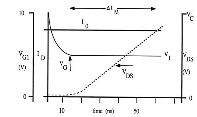
When the output at the gate driver goes to zero, the MOSFET's gate voltage decays exponentially, with the R-C time constant RG(CGS+CDG), to the threshold voltage (VG = Vt), where it remains for the miller time Atm. As drain current flows through the capacitors, VDS rises, causing a current to flow through the gate and the series resistance (RG). The current through the miller capacitor (CDG) is limited by the gate voltage. If more current were to flow, the gate voltage would rise, more current would flow through the channel, and less current would flow through CDG to the gate. Consequently, there is a feedback loop maintaining the gate at Vt while the
drain voltage rises.
The drain current splits between the two capacitors, in proportion to their relative sizes (q = CDG / CDS). Since the current in CDG depends on the gate current
(IG = V/RG), if this sum is less than the total drain current (l0), then the remainder
must flow through the channel while the drain to source voltage rises. Hence, a
19
larger gate resistance results in a smaller gate current, forcing more current through the channel and therefore greater dissipation.
In order to avoid this effect, the gate current must be large enough to allow all the drain current to flow through the capacitors so none will be dissipated. RG must be small enough so VG < Vt when all the drain current flows through the capacitors.
The total gate resistance includes the polysilicon gate and the driver resistance, so reducing RG involves reducing both components.
4 -- At -A 1u
-V
(V)
G
0-II
10
time (ns)
50
Fig. 2-4 Simulated turn-off response of the DMOS used in the case study. Miller time is represented in Fig.2-4, by AtM, as the time during which the gate voltage remains constant. Voltage rises across the device with a dV/dt determined by
the current through the capacitors and the combined value of CDG and CDS. Therefore, an average capacitance can be calculated for determining the miller time,
VOFF
Cavg = (VOFF -VON) 1 CDG(V) + CDs(V) dV .[2-1]
VON
ql II
Assuming the gate voltage remains constant at threshold (V), the gate current through the miller capacitor IG = Vt/RG. The ratio of IG to Is1 is equal to the ratio of
the capacitors, 9. The current lost to the channel resistance, therefore, is 1S2 = 0- IG - IS1 = 10 - (1+c VL [2-2]
Now, the miller time is calculated by assuming a linear capacitor Cavg with a constant current I0 - IS2 = (1+9) Vt/RG, giving a value for the miller time
AtM = [ RGCavg / (1+9)Vt] [VOFF - VON] .
[2-3]
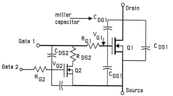
One additional characteristic of a discrete driver separated from the Gate is the appearance of a parasitic inductance. This inductance further limits the amount of cotrol one can achieve over the gate voltage. Fig. 2-5 shows the complete structure including the parasitic inductance. Changing the current through the inductor causes a parasitic impedance in series with the resistance, further enhancing the miller effect. The current can not be drawn out of the capacitor quickly, and more time is spent with current flowing through the channel during turn-off.
is Gate
Source
2.3. Integrating a turn-off driver
In an attempt to reduce the power dissipation due to the miller feedback effect of the turn-off portion of the switching cycle, we have decided to eliminate nearly all the parasitic inductance and reduce the gate resistance by integrating the turn-off gate driver on the power device. Such an integration could minimize the separation between the switch and the driver as well as reduce the gate resistance to an arbitrarily small value.
Gate 2
C DS1
Fig. 2-6 Modified DMOS structure with an integrated turn-off driver, showing all the parasitic elements.
The gate of a typical DMOS is made of heavily doped polysilicon. The conductivity of this material is lower than 1% of aluminum and typically dominates the value of the total gate resistance (RG). A driver integrated within the DMOS itself can be placed in a way which substantially decreases RG. The total gate resistance can be made small enough to keep the device OFF while current flows through the miller capacitor. During the miller time, the gate voltage will be below threshold and no power will be dissipated in drain - source resistance. Fig. 2-6 shows the
proposed DMOS structure with an integrated turn-off driver, including all its parasitic elements.
When the full current flows through the gate (Gl), the series resistance (RGT RG1+ RDS2) yields a positive voltage drop. If the total gate resistance were small enough, such that when the maximum miller current flows, the gate voltage stays below threshold (VG < Vt), then the channel would remain off while the drain to source voltage rises. Consequently, the entire drain current increases the voltage across the capacitors, while no current flows through the resistive channel during the plateau time
AtM = ( Cavg/I) (VF F- VON) . [2-4]
No power is dissipated in the channel as long as IG RGT < Vt. As compared to Eq.
2-3, there is no dependence on RG or 9 for a sufficiently small series resistance.
Therefore, with the value of the total series resistance
RGT 5 (1-9) Vt/ 10
[2-5]
including the driver, the gate poly, and the series impedance, the device is off, and no energy is dissipated in the channel during turn-off.
23
10
VG (V) 0-IIE
2
time (ns)
10
Fig. 2-7 Calculated current and voltage transient response of the modified DMOS with an integrated turn-off driver.
For the case device and circuit considered in this study, 10 = 1A and Cavg =
40pf. The values for Vt = 4.5 V and 9 = 0.8 as calculated from the geometry of the designed structure. The gate resistance, including the on-state resistance of the shorting switch RGT = 3 92. Thus the criterion of eq. 2-5 is met and the power dissipation, due to the miller feedback effect, is eliminated. Fig. 2-7 shows the resulting waveform for a transition from 1 to 150 V, with the turn-off time calculated from eq. 2-4. AtM = 10 nS, which is an improvement by almost a factor of 5 over the same structure with a discrete driver.
CHAPTER III.
DESIGN DETAILS
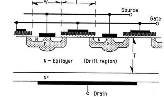
The structure of a basic vertical n-channel power MOSFET is shown in Fig. 3-1. A lightly doped epitaxially grown n-type layer of silicon on top of a low resistivity n+ substrate forms the drain of the device, and a patterned n+ polysilicon on a 1000A oxide forms the gate. The source and p-well diffusions are implanted through openings in the gate material, assuring their alignment to the gate edges. The channel forms in the p-type material just beneath the gate, between the n+ source and the n- epi-layer.
ýý W L -;p1
N - Epilayer (Drift region)
N+
SDrain
Fig. 3-1 Cross section of a typical Vertical DMOS showing the dimensions of the gate (L), the source well opening (W), and the epi thickness (T). The p-wells, which contain the n+ sources, are arranged in a matrix as seen from the top of the device in Fig. 3-2. The individual sources are interconnected with a continuous layer of metal that is deposited over the surface of the device. This metal is electrically isolated from the gate by a 1.5 gm thick layer of oxide. The metal also shorts the source (n+) regions with the p-wells at every contact in order to
25 avoid the detrimental effects of a floating substrate. To provide a low resistance path from the channel to the contact, the center of the p-well is heavily doped.
The channel region is self aligned to the gate by diffusing the p-well through openings in the poly. This approach minimizes the gate's overlap of the source, and therefore keeps the gate -source capacitance small. It also allows the design for the gate to be built into the same mask as the one used to incorporate the p-well, eliminating the need for alignment tolerances in the mask which defines the gate, keeping the dimensions small, and the fabrication process simple.
--
W --
L -00 --
*1
P
14-WM
poly
gate
W = 20 gm L = 14.5 lm P = 9.3 ltmW
= 12.7
glm
OX
W = 3.7 glm MTFox=
1.5
gtm
Tpoly
1.5
gm
Tpw
4
Lm
TN+ = 1.2 lim To = 975A
Fig. 3-2 Some typical dimensions for a 200 V vertical power DMOS. The p+ diffusion in the center of the source well is not typically self aligned in commercial power MOSFETs. This diffusion is instead introduced early in the
fabrication sequence, before the gate poly deposition. The openings for the source diffusions through this poly must therefore be aligned to the deep p+ regions. As a result, the design tolerances for the process steps that follow must be large enough to accommodate the spread of the p+ region. The well width (W) should be as small as possible, however, its minimum dimension is limited by the lateral diffusion of the p+ diffusion and the subsequent alignment tolerances.
The individual source wells are typically arranged as hexagons or squares within the polysilicon gate matrx. The source forms an annulus within the p-well, leaving the center open for the metal to contact the p+ region. The arrangement of these source wells within the poly determines the device geometry. Early investigations have shown that there is no significant difference in on-state resistance between a hexagonal geometry (Fig. 3-2), and a square geometry (Fig. 3-3).4
'7/
Fig. 3-3 Detail of the first mask layer defining the double diffusion within the region of side W, and the p+ contact made through the region marked P.
Hexagonal structures, on the other hand, have later been shown to give a slightly lower resistance for a given area than square ones. The effect, however, is second order (< 5%) and only becomes apparent with high current densities.5 Also, the optimal spacing between well widths (L) is independent of the geometry (square or hexagonal), so a square geometry will suffice for investigating the optimal values
27 of L for a given W. It is also easier to fabricate masks for the square geometry with the CAD facility at MIT.
The chip area used by the p-wells is not fully available for current to flow down the epi-layer. The electrons flow from the source, through the channel, and down to the n+ drain. The current spreads out under the p-wells at approximately 450 angles as shown in Fig 3-4. Narrower p-wells therefore increase the area available for conduction and provide a lower resistance for the same amount of area. The dimension of the source well, therefore, must be as small as possible to maximize the ON conduction for a given total device area.
The significance of this effect depends on the thickness of the epi as compared to the width of the p-well. Since the width (W) is made as narrow as lithography allows and the epi thickness depends on the off-state voltage of the device, the on-state resistance varies much more with the p-well width in lower voltage devices than in higher voltage devices. For example, the depth of the p-well is approximately 4 pm, and the width is 26 gm in a common commercial device. In a 150 volt device the epi is about 15 gm thick, so the current paths of adjacent cells do not even meet at the n+ substrate. Consequently, the on-state resistance of devices designed to withstand voltages in this range or lower depends greatly on the p-well width (W).
T
1Pm
4
L
-I-*-W/2
-o-Drain
Fig. 3-4 Cross section showing the current flow path of a typical 150 V DMOS.
When a sufficiently positive gate voltage is applied with respect to the source, the p-region beneath the gate inverts and forms a channel which turns the device ON. The surface of the n-region between the p-wells also goes into accumulation with the same gate voltage. The surface of the silicon thus becomes more conductive with the accumulated charge, allowing the current to spread out between the p-wells at the surface (Fig. 3-4). However, this effect is limited. Once the lateral surface conductance becomes comparable to the vertical conductance of the bulk epi, the current no longer spreads out, but flows downward instead.
Consequently, for a given epi thickness (hence a particular breakdown voltage), there is a particular p-well separation (L) which yields a maximum use of the area between the p-wells. This value should also be independent of W since it is a measure of the effectiveness of the current spreading. One can model the spreading resistance with a two dimensional model to determine an optimal value of L for a given breakdown voltage. Hower et. al.5 has investigated the optimal p-well spacing
29
for both a 120 V and a 500 V device. Their results confirm the geometries used in the 200 V commercial device shown in Fig. 3-2.
4- L
j
4-W / 2--T
15
15
VDS
10 V
50 V
120 V
Drain
Fig. 3-5 Cross section of an OFF device showing the depletion depth with various applied drain to source voltages
When the power MOSFET is off, on the other hand, a depletion region forms within the epi-layer and spreads across the device area. For voltages as low as 10 V, this depletion layer width is nearly independent of the source well geometry, as shown in Fig. 3-5. The capacitance caused by the depletion of the OFF device is thus nearly independent of the geometry and approximately proportional to the total device area. Consequently, if a given area is chosen for a desired on-state resistance, the off-state capacitance will be nearly directly related to it, independent of the p-well geometry. If W were decreased to yield a lower resistance, less area is needed, so the off-state capacitance will be smaller for the same desired ON resistance.
Some typical dimensions for a 150 V power DMOS are shown in Fig. 3-2. These values are shown for a hexagonal geometry, but should suffice for a "first guess" with a square geometry. The epi-layer is 2 92-cm n-type material with a
L
thickness of about 15 lm, which will withstand the full reverse voltage as long as field guard rings provide sufficient termination at the device edges.
The field guard rings surround the active device area as shown from the top and in cross section in Fig. 3-6. These p-type rings help spread out the equipotentials near the device edges to avoid premature breakdown. The rings are usually introduced with the p+ diffusion, early in the fabrication process, before the poly is deposited. On top of the guard rings, a thick isolation oxide must be grown or deposited so metal or poly from the main device will not interfere with the field termination.
Field guard rings
Device area
p+ Field guard rings
Fig. 3-6 Top view and cross section of p-type guard rings surrounding the active device area which provide field termination at the edges.
The following two sections of this chapter describe the way the process and masks are designed to reduce the capacitance for a given on-state resistance, and how a secondary lateral MOSFET integrated on the main device structure is a turn-off driver. Some of the design considerations which lead to the fabrication sequence and mask set are discussed. Also, the structure which has been fabricated at MIT is detailed. Finally, the last section provides calculated resistance and capacitance values for the completed structure.
3.1. Decreasing the on-state resistance
One can achieve a source region with the smallest possible W by having both a p-well that is self-aligned to the gate and a p+ contact region that is self-aligned to the
center of the n+ annulus. The first mask, which defines the gate poly, the p-well, and the n+ source, can also define the opening in the center of the well as shown in Fig 3-7. This process takes advantage of the selectivity by which silicon can be etched with respect to oxide in a controlled plasma. The center region of width P is removed after the double diffusion of Boron (p-well dopant) and Arsenic (n+ dopant) to define the implant for the p+ contact.
Resist Poly SBoron
implant
Resist
Oxide
n+ n+p+
Fig. 3-7 cross sections showing double self-aligned process. a) The first mask patterns the poly for the p-well diffusion and the n+ implant. b) The poly at the center of the region is plasma etched and the heavy boron dose is implanted. c) The final diffusion step forms the junctions.
The heavy p+ Boron must diffuse beneath the n+ region, so a high temperature step follows that final implant. However, the n+ diffusion can not be allowed to diffuse more than 1 gm under the gate, otherwise the channel will be too narrow. At lower temperatures, the diffusion constant of Boron is higher than that of Arsenic2, so the n+ region will not diffuse as far as the p+ region. Thus, a long
diffusion at a lower temperature after both the n+ and p+ implants have been made will allow the Boron to diffuse farther than the Arsenic. The p+ region is more
a)
33 lightly doped than the n+ region which insures that the n+ region will contact the source metal. The Arsenic profile is what limits this final diffusion, thus, the final diffusion step should be adjusted for the ljtm junction between the n+ and the p-well, without concern for the p+ profile. Also, there should be no high temperature processing steps between the n+ and the p+ implants to insure a maximum diffusion
of the p+ "plug" region.
Along with the implant for the source double diffusion, guard rings are defined for field termination at the edges of the devices. The p-well diffusions, used for the p-region of the "rings", consequently have n+ at the surface (Fig 3-8). This occurs because there is no masking step between the p-well diffusion and the n+ implant. Since they basically provide equipotential regions around the active device area in the OFF state, there is no trouble with isolated n+ regions at the surface. These diffusions are also aligned to the rest of the device since the first mask defines all the structures. A plasma can etch poly in a selective and anisotropic fashion giving straight sidewalls, accurately transferting the mask pattern and stopping at the underlying oxide.
and
Ion implant
w/ -
o
I
y
l
-ep-typeguard
ring
Fig. 3-8 Double diffusion and guard ring placement, defined with the first mask.
The best way to determine the optimum dimensions of the power MOSFET is to fabricate a matrix of devices on the same chip and compare their characterisics on a
flResist
one-to-one basis. One of the devices with the smallest W should have the lowest on-state resistance, but it is not clear what the optimal value of L will be for that well width. Secondly, it is not clear how reliably the devices with the smallest W can be produced. Hence, in order to determine the geometry which consistantly yields the lowest ON resistance for a given area of silicon, a matrix of devices with various values of W and L have been chosen around the values which were determined as optimal from two dimensional models.4-8 Fig. 3-9 shows the layout of the chip with
LO c c 4~ S j II CNj Id- (C co F -4 0 0 4)) 4 4 do bi )C 0 .5 4) L_ T-o II .0 6o o 0 . '0 ..4o 4o O '0q ). . E4 -'0 c Fi V- 1- V- T- i u 4 4)9 "-I L 4) '0Cce C o .. 44 C.) .$ I= '0 4-44bIbi C4 Crl
high voltage device, as long as the gate of the shorting switch is narrow enough for the lateral p-well diffusions to join from either end. Fig. 3-10 illustrates how the driver is incorporated within the main device with 4 gm wide gates on either side of the n+ sources. The isolated n+ diffusion between the two gates (G2) acts as the drain of Q2 and must be electrically connected to G1. The lateral spread of the n+ diffusion under the gate is 1 gtm, while that of the p-well is 3 gtm, giving a 2 gm channel length for the device which will be used as the integrated turn-off driver.
Gate 2 -4 Source
Gate
1
oNQ2
Q1 N+Drain
Fig. 3-10 Cross section of the integrated driver, housed in an extended p-well within the basic DMOS structure.
This arrangement allows the driver to be routed around the chip in order to achieve sufficient channel width (Zch). The lateral MOSFET must occupy as much area as needed for its full ON resistance, plus the resistance of the main device's gate poly, to meet the criterion of eq. 2-5 (409 for the device of this study).
For the designed device, the voltage at the gate G1 must be able to withstand 20 volts without breaking down or punching through. Since the channel length is 2 gm, the p-type doping must be 1017 cm-3 at the surface of the well.1 If the doping is
much less than that, the drain of Q2 will reach through to the source, and the gate
37
voltage will not be able to go higher without current flowing to the source. Similarly, if the doping were made much heavier, the p-n junction would break down due to normal avalanching.
The thresholdvoltage of both the shorting switch and the main device will be the same since they are formed by the same diffusions and have equal surface doping concentration and gate oxide thickness. Assuming this concentration is
approximately 1017 cm-3
and the oxide thickness is 1000A, the threshold voltage Vt should be around 4.5 volts. For voltages greater than this, inversion charge accu
-mulates at the silicon surface, and the total charge in the channel (Qch) is approximately
Qch = Cox [VG - Vt] [3-1]
where Cox is the gate oxide capacitance per unit area. Knowing the inversion charge for a given applied gate voltage and the channel mobility (gch), the resistivity in 9/' is
Rch = (ch Qch )-1 [3-2]
The inversion charge is directly proportional to the applied voltage, and therefore the E-field, but the mobility is not. The dependence of the channel mobility on transverse E-field (Ex ) is approximately linear for Ex between 2 and 8 x 10⁵
V/cm. Experimentally determined values for tch verses Ex at room temperature,
within these limits, can be fit into the following relation, tch = 700 - 5.56 x 10-4 E
x [3-3]
Ex
=
(VG
-
V)/Tox
A quadratic relation results in which Rch is minimized when Ex = 6.3 x 10⁵ V/cm.
Raising the gate voltage above this point only decreases the channel conductivity. Consequently, the gate voltage which minimizes the channel resistance is approximately 10 V, resulting in a minimum channel resistance of
Rch , min = 4500 2/13 . [3-4]
The resistance of the poly is the largest portion of the total resistance from the gate G1 to ground. This total resistance must be 4 Q2 or less for the designed device. The area of the whole device is 1mm x lmm to achieve the desired 0.5 Q ON resistance from the drain to source of Q1, as required by the circuit of the case study (Ref. Chapter 2). Assuming 12 92/Dpolysilicon, and a minimum distance between metal contacts of 0.5 mm, the total gate poly resistance can be approximated for the
lmm x lmm device.
By assuming that half the area is insulated, the effective sheet resistance is twice that of a sheet of poly. The number of squares can be conservatively approximated as half the width of the gate area divided by the perimeter. Since the distance to the center is 0.25 mm and the perimeter is 6 mm, there are 1/24 squares. Therefore, the resistance is 1 9 by a conservative estimate, so to achieve a minimum ON resistance of less than 2 K2, the total channel width Zch must be larger than 0.9 cm.
39
G2
poly
Guard
rings
-IFig. 3-11 Basic scheme for incorporating the driver around two blocks of DMOS.
The chosen configuration, as illustrated in Fig. 3-11, has two blocks of DMOS surrounded by double shorting switches. Each block is 1mm x 0.5mm, and the extended p-wells contain two gate lengths. The center of the two blocks has a row of four G2 lines separating them. The total effective channel width is therefore
Zh = 1.2 cm
Since the channel length is 2 gm, the minimum ON resistance with 10 volts at G2 is RON, Q2 = 0.75 Q
which makes the total gate resistance less than 2 Q2 from the gate to ground when the driver is ON, as long as the connections with the metal make contact with a low enough resistance.
II
-Fig. 3-12 A detail of a single DMOS with an integrated shorting switch showing the interdigitated metalization scheme connecting the source and gate to the driver.
In order to achieve a minimal resistance from G1 to the shorting switch, the metal contacts must be interdigitated as closely as possible. Fig. 3-12 illustrates how the metal connects over the shorting switch. A close-up of the center portion is shown in Fig. 3-13. The contacts are made through the field isolation oxide. Long fingers down the middle of the device contact the poly gates on either side to each other and to the n+ diffusion in the center of the shorting switch (drain of Q2).
3uard rings Gate 1 metal Source metal Gate 2 poly Metal separation Gate 2 metal
a
G1 poly p+ n+ contact vias
II: 'I i I G2 ii , • 1 ;', , t i ~ ~ , I / z' ,,: S'/' ,Source m // ,G1 metaK //, .: //, / • I' , / i / / i 0 / /It ' t' /I , t /I i
/
~,
~i,
~i
,/
I
Fig. 3-13 Metalization detail in the center of the device. how the double shorting switch is incorporated.
I· ,
· ,
i I I i i I r i I iI i I i iI IIII I I i ( I I ,Ii I I ItI iI
ThisXt
illustratesCalculated properties of the design
To approximate the resistances and the capacitances of the total structure, certain assumptions must be made about the device. First, each device in the 4 x 4 matrix is assumed to have only slightly different dimensions. Second, the actual values of the on-state resistance cannot be accurately modeled, so for the purpose of determining the approximate properties of the designed devices, a single case example will be used, one which should be optimized for high conductiviy per given area. The dimensions for this case example are L=16 grn, and W=8 gm. The single device contains N=1600 source wells in the 1mm x 1mm area.
a .
The on-state resistance of the main device can be calculated by determining the conductance per source cell, multiplying it by N, and then inverting the result. The length of the p-well on one side is the opening (W) plus the lateral diffusion on either side (6gm). This makes the total p-well width (s1) equal to 14 gm, for this example, and the separation between the p-wells (lc) equal to 10 gm. Referring to Fig. 3-14, the total resistance includes the channel resistance Rch, the resistance due to the lateral current flow in the accumulated n-region R1, the resistance due to the vertical path
between p-wells R2, and finally, the resistance due to the spreading under the p-wells
R3.4
The channel has the same sheet resistance as the shorting switch: 4500 2/ . The total channel resistance is therefore 0.1 9. R1 and R2 may be combined, and
approximated as a single resistance contribution5,6 whose resistance equals
approximately 0.1 Q. Finally, the spreading resistance is calculated assuming a 45 o spreading angle beneath the p-well regions. Assuming the gate over the n-region encompasses 65% of the total device area, the relative resistance has been calculated as a ratio of R/Ro = 1.2, where Ro is simply the resistance of the bulk epi.7 The epi
is 2 92-cm material, and there is a 10 gm separation between the p-well junction and the n+ substrate, making R3 = 0.24 0. Thus, the total on-state resistance for the
43
oxide
n+
ol Gate
GS
Fig. 3-14 Cross-section of the vertical DMOS showing the resistances and the capacitances for the main structure
The gate area is what determines the relative input capacitances of the two MOSFETs. These are found for the 1mm x lmm device, where area of the main device is
AG1 = (lmm)2 - N(W)2 = 9.0 x 10⁻³ cm2 [3-5]
similarly, the area of the shorting switch gate (G2) is
AG2 = (12mm) x (41gm) = 0.48 x 10⁻³ cm2 [3-6]
which is simply the total length times the width of the driver. The input capacitance to the driver is thus approximately 5% that of the main device. This is important when considering the speed at which the device can turn on and off. The RC time
constant of the driver, which determines the minimum time needed to create the channel, is
tRC = Cox Rs,poly (1G2/8)2 [3-7]
where Rs is the sheet resistance of the poly, and 1G2 is the length of G2. For the
designed device, this product is approximately 2 ns.
The drain - source and the drain - gate capacitances will now be calculated.
They are both strongly dependent on the device area and not on the source cell geometry. Their values are significantly larger when the device is ON and the depletion region is narrow than when the device is OFF. Both capacitances follow a V-1/2 dependence with the Drain voltage since the depletion width primarily determines the total capacitance. As described in Chapter 2, the relative values of CDs and CDG (the miller capacitor) are nearly constant by a factor 9. This geometrical factor relates the area beneath the p-well to the surface beneath the gate in the n-layer. The results for the device are summarized for each steady state (ON and OFF):
State VDS CDS CDG
ON 1 volt 100 pf 240 pf
OFF 150 volt 3.4 pf 6.6 pf
Finally, the gate - source capacitance calculation considers the driver's contribution to the total capacitance. Fig. 3-15 illustrates the device cross section including the driver. The contribution to the gate - source capacitance from the shorting switch is shown schematically as CGS"'. This capacitance depends strongly on the gate (Gl) - source voltage and must be added to the contributions from the isolation oxide and the gate overlap, as shown in Fig. 3-14 (CGs' and CGSi").
45
Fig. 3-15 cross section showing the final metalizatin, indicating the depletion capacitance contribution form the driver.
The isolation oxide thickness is approximately 1.5 .tm thick over the entire structure. Assuming the area of this capacitor as AOl gives a value of CGs' = 21 pf. Similarly, the fixed capacitor due to the the overlap of the gate poly with the p-well diffusion yield a value CGS" = 66 pf. A more rigourous calculation is not necessary since these capacitances are nearly independent of voltage, and they are generally small by comparison to the depletion capacitance of the shorting switch.
Depletion in the shorting switch only occurs beneath the drain of Q2 since the source is shorted to the p-well, so the area of concern is the junction of the n+ diffusion with the p-well. The calculation assumes a uniform doping of 1017 cm-3 with an area of 12 gm wide and 12 mm long and a uniform, one-dimensional depletion layer. When the main device is ON, the gate voltage (Gl) is high at 10 V and this capacitance is found to be 39 pf. The value increases with (VG1 - 1)-1/2 to its
maximum capacitance of 130 pf. Thus, summing the three components of the Gate to Source capacitance together yields:
State VG1 GGS
ON 10 volts 126 pf
OFF 0 volts 215 pf
CHAPTER IV.
THE FABRICATION PROCESS
Each high temperature step in the fabrication process increases the likelihood that impurities will enter the wafer. In order to minimize extraneous contamination, the process sequence uses the fewest possible number of diffusion steps by combining the drive-ins of the n+ source and the p+ contact into the same step. This approach allows the p+ plug, which is self-aligned to the source cont-:t, to be diffused only a small amount. It is only driven in with the final diffusion step, so it does not spread any farther than about 2.5 pgm under the source diffusion. The n+ region is also more heavily doped than the p+ region so the metal will make a good contact to the source and the p-well. The source and p-well can thus be made much smaller than is typical for devices where the p+ contact is driven in first.
Since the p-wells and sources are self-aligned to the gate, the gate oxide growth and the polysilicon deposition must take place before any of the dopants are implanted and diffused. The fabrication thus begins with lightly doped n-type silicon epi wafers on (100) n+ silicon substrates. The epi is of the thickness and resistivity needed for standing off the 150 V required. Aside from the epitaxy, high temperature steps include: oxidation, polysilicon deposition, p-well diffusion, n+ and p+ diffusion, and deposited oxide densification. Other steps, including oxide deposition, are performed at temperatures below 500 OC where they do not contribute significantly to dopant diffusion or wafer contamination.
The following five sections of this chapter discuss details of the fabrication sequence. The appendix contains a complete step-by-step proceedure for fabricating
47 the actual devices whereas this chapter discusses the purpose of each step in the overall process.
First, the gate oxide is grown and polysilicon is deposited. The poly is then patterned and plasma etched to form the basic structures. Boron is implanted through the openings and then diffused to nearly its final depth in the silicon. Through the same openings, Arsenic is implanted but not driven in. The poly is also doped with the arsenic by the same implantation.
The poly surrounding the active device area, and between the field guard rings, is then removed by a second plasma etch, through openings defined by the second mask. At this point, the poly is doped, so it has a different etch rate than pure poly, hence the etch rate must be monitored before each run.
A 1 gm layer of oxide is then deposited over the structure and patterned with the third mask. Openings to the contact plugs, through the oxide, help align the final poly etch. Once the oxide over the plugs and the poly have been etched, the oxide over the rest of the wafer protects the poly from the deep Boron implant meant to be the p+ contact diffusion. After this implant, the oxide is removed so a final isolation oxide deposition will be uniform over the wafer. The oxide is then densified with the long diffusion at a low temperature (1000 OC) in a nitrogen ambient.
The wafers are then completed by defining and etching the contact vias with the fourth mask followed by the metalization with aluminum. The metal is then patterned and etched using the fifth mask and the backside of the wafer is prepared and metalized.
4.1. Gate oxide and polysilicon
The growth of 1000 A of gate oxide on a prepared and cleaned epi wafer as the first process step insures that no sodium or other bulk impurities will be introduced into the oxide from a previous diffusion. Immediately following the oxidation, gate polysilicon is deposited by low pressure chemical vapor deposition (LPCVD). This passivates the oxide by encapsulating it between the silicon epi and the polysilicon gate. Also, if the wafers go directly from the oxidation furnace to the poly furnace, the likelihood of impurities being introduced is further decreased.
Once the wafers have been properly prepared for oxidation, and the furnace and boat have been cleaned in an HCl environment for at least 1 hour at 1100 OC, the wafers are loaded on the boat and put into the furnace. The parameters for growing 1000
A
of gate oxide have been experimentally determined for the furnace in the microfabrication laboratory at MIT to be 46 minutes at 1100 oC in dry oxygen. This process was first performed on test wafers which were then measured to have oxide thicknesses of 1020 + 30A,
a sufficient value for the desired gate oxide.During the oxide growth, the polysilicon furnace is prepared for the 1 gm deposition. When the growth is completed, the wafers are brought to the mouth of the oxidation furnace where they remain in the nitrogen flow until they can be loaded into the poly furnace. This insures that they do not become contaminated between the two steps. The wafers are then loaded onto the boat of the poly furnace, without delay, after being withdrawn from the oxidation furnace. No wafer cleaning is needed between these two steps.
49
...
. . . .
t
T
=1gmJ±
poly
:f:::::::I~f::i~::::::iS~::iP Y~
= I UUUAoxide
epi
region
Fig. 4-1 Cross section of the device with the gate oxide and polysilicon. The structure at this point is shown in Fig. 4-1, where the 1000
A
of gate oxide on the n- silicon epi is covered by 1 gm of polysilicon. This sandwich is patterned by the first mask and the photo-resist alone is what masks the poly for the plasma etch. The wafers are etched in a Freon plasma in the LAM plasma etching system, where silicon is selectively removed. The etch rate of polysilicon is nearly five times that of the underlying oxide, so the process is essentially self stopping at the oxide under the poly. This process step is further described in section 4.4.4.2. Double diffusion
The p-well and the n+ source are both implanted through the same openings created by the first lithographic step. The Boron must first be diffused in deeply enough so there will be sufficient isolation between the drain and the source after the second diffusion (Fig. 4-2). The second diffusion must drive in the p+ contact region as deeply as possible while not allowing the n+ source to diffuse lateraly more than 1 gm. Since the diffusion coefficient for Arsenic is approximately 5 times smaller than that of Boron at 1000 OC, the second diffusion step will be done at this temperature for long enough time to make the junction between the n+ source and the p-well occur 1 gm laterally under the gate.
'""^~