HAL Id: hal-02045474
https://hal.archives-ouvertes.fr/hal-02045474
Submitted on 3 Mar 2019HAL is a multi-disciplinary open access archive for the deposit and dissemination of sci-entific research documents, whether they are pub-lished or not. The documents may come from teaching and research institutions in France or abroad, or from public or private research centers.
L’archive ouverte pluridisciplinaire HAL, est destinée au dépôt et à la diffusion de documents scientifiques de niveau recherche, publiés ou non, émanant des établissements d’enseignement et de recherche français ou étrangers, des laboratoires publics ou privés.
Gas Phase Synthesis of Multifunctional Fe-Based
Nanocubes
Jérôme Vernières, Stephan Steinhauer, Junlei Zhao, Audrey Chapelle,
Philippe Menini, Nicolas Dufour, Rosa E. Diaz, Kai Nordlund, Flyura
Djurabekova, Panagiotis Grammatikopoulos, et al.
To cite this version:
Jérôme Vernières, Stephan Steinhauer, Junlei Zhao, Audrey Chapelle, Philippe Menini, et al.. Gas Phase Synthesis of Multifunctional Fe-Based Nanocubes. Advanced Functional Materials, Wiley, 2017, 27 (11), pp.1605328. �10.1002/adfm.201605328�. �hal-02045474�
1 DOI: 10.1002/ ((please add manuscript number))
Article type: Full Paper
Gas Phase Synthesis of Multifunctional Fe-based
Nanocubes
Jerome Vernieres, Stephan Steinhauer, Junlei Zhao, Audrey Chapelle, Philippe Menini, Nicolas Dufour, Rosa E. Diaz, Kai Nordlund, Flyura Djurabekova, Panagiotis
Grammatikopoulos and Mukhles Sowwan*
Dr. J. Vernieres, Dr. S. Steinhauer, Dr. R. E. Diaz, Dr. P. Grammatikopoulos and Prof. M. Sowwan
Nanoparticles by Design Unit, Okinawa Institute of Science and Technology (OIST) Graduate University, 1919-1 Tancha, Onna-son, Okinawa 904-0495, Japan
E-mail: mukhles@oist.jp
Dr. J. Zhao, Prof. K. Nordlund, Dr. F. Djurabekova
Department of Physics and Helsinki Institute of Physics, University of Helsinki, P.O. Box 43, FI-00014 Helsinki, Finland
Dr. A. Chapelle, Prof. P. Menini, Dr. N. Dufour
LAAS-CNRS, Université de Toulouse, CNRS, UPS, 7 avenue du Colonel Roche, 31031 Toulouse, France
Fe nanocubes, magnetron sputtering, gas sensor, magneto-plasmonic, molecular dynamics
Magnetron-sputtering inert-gas condensation is an emerging technique offering single-step, chemical-free synthesis of nanoparticles with well-defined morphologies optimized for specific applications. Here, we report a flexible approach to produce Fe nanocubes as building
blocks for high-performance NO2 gas sensor devices, and hybrid FeAu nanocubes with
magneto-plasmonic properties. Considering that nucleation happens within a short distance from the sputtering target, we utilize the high-permeability and resultant screening effect induced by magnetic Fe targets of various thicknesses to manipulate the magnetic field configuration and plasma confinement. We thus readily switch from bimodal to single-Gaussian size distributions of Fe nanocubes by modifying their primordial thermal environments, as explained by a combination of modeling methods. Simultaneously, we obtain a material yield increase of more than one order of magnitude compared to
2
experiments using post-growth mass filtration. The effectiveness of our method is demonstrated by the deposition of Fe nanocubes on microhotplate devices, leading to unprecedented NO2 detection performance for Fe-based chemoresistive gas sensors. The
exceedingly low detection limit down to 3ppb is attributed to a morphological change in
operando from Fe/Fe-oxide core/shell to specific hollow-nanocube structures, as revealed by
in situ environmental transmission electron microscopy.
1. Introduction
Over the past decades, metallic nanoparticles (NPs) with optimized morphologies have attracted significant interest in research areas such as catalysis,[1,2] hydrogen storage,[3]
biomedicine,[4] plasmonics[5,6] and gas sensing.[7] In particular, the unique size- and shape-dependent electronic, magnetic and optical properties of NPs and their assemblies[8] have led
to various emerging technologies of functional devices[9] ranging from reconfigurable
Boolean logic[10] to novel types of biosensors[11] and chemoresistive gas sensors.[12,13] For the latter application, the development of scalable nanomaterial fabrication techniques that are
compatible with industrial complementary metal-oxide-semiconductor (CMOS)
manufacturing is of utmost importance for successful gas sensor commercialization and incorporation with integrated circuit technology. In this regard, inert-gas condensation approaches are ideally suited, as they allow single-step NP deposition at room temperature under high-vacuum conditions, resulting in high chemical purity due to the absence of organic solvents.[14,15] Furthermore, by using a versatile magnetron sputtering synthesis method,[16] NPs with well-defined size, chemical composition, and crystalline structure can be achieved,
which is a crucial prerequisite for optimized gas sensing[17] or nanoplasmonic
characteristics.[18] For many important systems, however, NP gas-phase synthesis techniques have been facing low material yield[19] as a major obstacle to high volume production for
3
technologies.[20,21] Regrettably, precise size control has always been associated with
post-growth NP separation such as time-of-flight or quadrupole mass filtration,[19,22] which inevitably leads to a reduced quantity of deposited NPs. In order to overcome these limitations, advances in understanding NP formation are required for further improvement and technology up-scaling of NP gas-phase synthesis.
To this end, we recently investigated the growth mechanism of Fe NPs of switchable shapes, and demonstrated the decisive kinetics effects that give rise specifically to anisotropic, cubic morphologies.[23] Here, we tackle the issue of precise simultaneous control over size and chemical composition, as well as shape, while maintaining high-uniformity and consistently sufficient material yield. We present an in-depth study on Fe nanocube synthesis and their application in high-performance gas sensing devices, and explore the possibility for additional functionalities by doping with Au. Introducing the magnetic target thickness as a new experimental parameter to manipulate the plasma density and distribution near the target surface ensures precise control of NP size and morphology during growth, rendering subsequent mass filtration obsolete. A material yield increase of more than one order of magnitude is thus obtained, which, coupled with the well-known preferential head-to-tail alignment of the magnetically anisotropic cubes,[24] enables the realization of percolating Fe nanocube thin films as low-cost material for chemoresistive gas sensing. We report on the low
ppb-level range detection of NO2 (down to 3ppb), which is, for instance, relevant for
biomedical applications (i.e. exhaled breath analysis) and for atmospheric air pollution monitoring.[25] Compared to previously reported in Fe-based sensors,[26] our devices show
unprecedented sensor performance, while comparing favorably with the vast majority of literature reports on NO2-sensing using inorganic materials such as 1D metal oxides[27] or 2D
materials[28]. In contrast to other currently available nanofabrication techniques, our NP synthesis method simultaneously offers simplicity, scalability and CMOS-compatibility due
4
to room-temperature deposition, making Fe nanocubes realized by magnetron sputtering inert gas condensation ideally suited for gas sensing applications.
2. Thermal Environment Effect on Nanoparticle Morphology
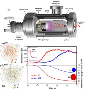
In a magnetron sputtering inert-gas aggregation system the sputter target is placed on the magnetron gun, and when aggregation gas (usually Ar) is fed into the chamber, plasma is formed by ionization due to electrical discharge (Figure 1a). Subsequently, Ar+ ions bombard the target, sputtering atoms off its surface. Unlike conventional sputtering, these energetic atoms collide with room-temperature Ar atoms, cool down, and, upon collisions with each other, eventually form nanoclusters.[29,30]
Figure 1. a) Schematic representation of a high-vacuum magnetron sputtering inert-gas
aggregation system. b) MD computer simulation representations of NP formation in systems
containing high (top) and low (bottom) Fe:Ar atomic ratios. Top graph: temperature
5
energy evolution of both systems, indicating a large number of small NPs in the former case,
compared to a smaller number of larger NPs in the latter, as shown by representative NP
insets.
There is a direct correlation between the morphology of the resultant clusters and the
thermal environment in which they were generated. NP temperature during growth is
governed by the relative rates between collisions with Ar and sputtered atoms; any variation in these rates may result in clearly distinct NP structures. In order to demonstrate this delicate effect of Fe:Ar ratio on Fe nanocluster growth, we applied molecular dynamics (MD) computer simulations with a model designed to correspond to the conditions of our experimental setup as closely as practically possible, within computational time and size
limits (Section 1, Supporting Information). In Figure 1b, exemplary MD results are shown
with sputtered species-to-inert gas atomic number density ratios of 1/5 (red curves) and 1/10 (blue curves), respectively, while maintaining equal total atomic densities. The top graph reveals typical temperature evolution profiles for both samples. An instantaneous initial temperature drop due to single Fe atoms colliding with room-temperature Ar atoms (inset) is followed by a heating phase due to Fe-Fe bond formations. Clearly, condensation of the high-Fe density sample started earlier (~0.3 μs) and led to a slightly higher maximum temperature. In both cases, when the simulation box eventually became depleted of Fe atoms, a maximum temperature was reached and the systems started cooling down gradually.[31,32] The growth rate of the nanoclusters is more clearly demonstrated in the bottom graph, showing the potential energy evolution of the Fe atoms. Decreasing potential energy is the fingerprint of bond formation; therefore, it is evident that aggregation of the high-Fe density sample was faster and more pronounced than that of the low-Fe density one. By the end of the simulation run, the overall potential energy decrease in the former model was double that of the latter,
6
corresponding to a smaller number of larger-size particles (only 3 compared to 11 in the low-Fe density sample).
Besides their effect on size, subtle differences in the thermal environment can also have a major effect on the shape of the NPs. The rate of atomic deposition on the growing nanoclusters in combination with their current temperature can determine the morphology;
decisive differences in kinetic growth modes give rise specifically to cubic rather than
near-spherical shapes.[23] Due to the sensitive correlation between growth conditions and the
resultant nanoparticles, in what follows special emphasis is given to determining the former as
accurately as possible, in order to predict and control the properties of the latter.
3. Magnetic Field Optimization via Target Thickness Modification
In magnetron sputtering, plasma confinement is achieved by locating a set of permanent magnets behind the target surface (Figure 2a). The resulting magnetic field acts as a secondary electron trap that modifies their trajectories into a cycloidal path, enhancing the ionization rate of the sputtering gas. Once a sputtering target is used, a groove (commonly referred to as the racetrack) starts forming, which modifies the magnetic field strength close to the target surface. A higher ionization rate occurs in this region due to an enhancement of the magnetic field.[33] This leads to a modification of the sputter yield,[34] influencing considerably the cluster size obtainable with the source.[35] When magnetic targets (Fe, Ni, Co, etc.) are used, they can affect the magnetic field configuration via a screening effect. This effect, arising from the high permeability of ferromagnetic materials, induces magnetic flux through the target, allowing only a small part to leak out and sustain the magnetron plasma. Therefore, if the magnetic field is adjusted via the magnetic target thickness, the electron
7
confinement (magnetic field distribution) and the plasma density (magnetic field strength) are modified, as demonstrated previously.[36,37]
In order to scrutinize the influence of the magnetic screening effect experimentally, Fe NPs were deposited onto silicon nitride transmission electron microscopy (TEM) grids using three Fe target thicknesses: 0.3mm, 0.5mm and 1mm. Typical low-magnification TEM
images reveal well-dispersed Fe NPs with a markedly high probability of demonstrating
cuboid morphology (average over 9 samples ~90%), as shown in Figure 2b. The Gaussian
distributions obtained in all cases clearly demonstrate that no coalescence or agglomeration took place during NP formation.
8
Figure 2. a) Schematic of the magnetron sputtering principle. b) Particle-size distributions
and representative TEM micrographs for the Fe nanocubes (Left: 0.3mm; Center: 0.5mm and
Right: 1mm target thicknesses). c) Finite Element Method (FEM) applied to a paramagnetic
Ti target (1mm thickness) compared to the three ferromagnetic Fe targets (d) Normal
components Bz of the magnetic field for all cases. e) Normalized profile measurements of the
groove after Fe nanocube depositions.
We quantified the screening effect induced by Fe targets of various thicknesses using finite element method (FEM) simulations of the commercial magnetron source utilized in this study(Figure S1, Supporting Information). For benchmarking we compared the magnetic flux densities for the cases of the ferromagnetic Fe targets with a paramagnetic Ti target (Figure 2c, top). Primarily, the magnetic field strength near the target surface, which dictates the plasma density, shows a gradual decrease with target thickness, especially for the 1.0mm Fe target (Figure 2c, bottom). Moreover, the magnetic field distribution is also drastically modified in the 1.0mm case due to the screening effect induced by the Fe target. The magnetic confinement of electrons is essential to the erosion of the target, since it governs the ionization of Ar atoms. In the cases of the paramagnetic target and the 0.3-0.5mm Fe targets (Figure 2c, second and third rows), the emitted electrons are confined tightly within the
electron trap region (Bz=0, indicated by the red circles in Figure 2b). In the 1mm Fe target
case, the electron trap region is shifted toward the center of the target, as shown in Figure 2c. This is clearly demonstrated in Figure 2d with a displacement toward zero (center position) of the Bz component of the magnetic field. Moreover, considering less efficient electron confinement due to the reduced normal flux density, a wider erosion region is expected. In order to obtain the erosion profile of each target, we performed profilometry measurements
9
after NP deposition using a Bruker DektaXT profiler instrument; clear evidence of the target
thickness influence on the racetrack width is demonstrated in Figure 2e.
According to the FEM results, the magnetic field strength close to the target depends on its thickness and controls the electron confinement; this, in turn, governs the width of the erosion profile and consequently the atomic density and temperature of the plasma zone, i.e. the thermal environment where nucleation and growth occur. In that sense, the well-defined narrow size distribution obtained in the 0.3mm case can be explained by the enhancement of the plasma density close to the target surface, with the electron confinement more localized in the direction perpendicular to the target surface[38] leading to a uniform thermal environment. In contrast, gradual increase of the target thickness induces a broader electron confinement along the direction parallel to the target plane and a decrease in uniformity of the thermal environment. The 0.5mm case confirms this tendency with a larger standard deviation compared to the 0.3mm case. Furthermore, in the 1mm case, a surprisingly well-defined bi-modal distribution is obtained, which signifies totally different plasma conditions, leading to the simultaneous creation of two distinct growth environments.
4. Quantitative Analysis of Nanoparticle Size as a Function of Sputtering Yield
In order to elucidate the growth behavior of the Fe nanoclusters under specific magnetic plasma conditions, we combined MD simulations with an analytical model and correlated the results with the groove profile measurements. We focus on the 1mm target as a case study, exploiting the well-defined bi-modal size distribution it exhibits.
The incidence angle, θ, of the energetic ions (Ar+) bombarding the target defines the
depth of the interaction volume between the ions and the target[39]. In the beginning of the
10
surface, leading to a change of the incidence angle and affecting the growth behavior of the nanocluster.[34] The aforementioned screening effect of the thick magnetic target led to the creation of an asymmetric racetrack. Two distinct angles were measured on the upper part of the groove in Figure 3a, namely θ1≈45° and θ2≈70°. MD simulations were utilized to calculate the sputter yield YFe as a function of the incidence angle for a constant Ar kinetic impact energy of 300eV (Figure 3b and Section 3, Supporting Information). Since experimental Fe targets are typically polycrystalline, three low-index {100}, {110}, {111} surfaces were simulated and the results were averaged (Figure 3c). It should be emphasized that this distinct difference in incidence angle between the two sides of the race track leads to a remarkable disparity in YFe: a 5-fold increase is obtained, with YFe[θ1]≈2.5, compared to
YFe[θ2]≈0.5 (Figure 3c), which induces a major modification of the Fe:Ar atomic ratio in two
11
Figure 3. a) Groove profile measurement after Fe nanocube deposition (1mm target thickness
case). The red area represents the approximate pre-sputtering region. b) Exemplary
simulation cell for MD simulations. c) Angular dependence of the sputtering yield at 300eV
ion energy. d) Calculated number of atoms in one Fe NP (N(t) as a function of time (t)) using
different initial density of Fe atoms (ρFe).
In order to explain the large difference in size of the bi-modal distribution obtained with the 1mm target, we developed an analytical model based on our previous studies[23,40] (Section 4, Supporting Information). It is clear from Figure 3d that there is a superlinear dependence between the number of atoms in one cluster and the Fe atom density. A 5-fold difference of Fe atom densities (ρFe1 and ρFe2, estimated from the sputter yields mentioned
12
good agreement with the ratio calculated from the NP sizes of the bi-modal distribution (Section 4, Supporting Information). Furthermore, the NP size difference between the 0.3mm and 0.5mm targets can be correlated with a slight variation of the incidence angle (Figure S2, Supporting Information).
Similarly to our model, previously suggested mechanisms for the creation of bi-modal
distributions of nanoparticles grown under plasma conditions also focus on the presence of
inhomogeneous nucleation and growth regions. Studying the synthesis of Cr nanoparticles,
Yamamuro et al. correlate the Ar gas pressure in the chamber with the width of the growth
region, which, under certain conditions, can become inhomogeneous.[41] Koten et al., on the
other hand, speculate on the formation of an initial distribution of Cu nanoclusters with a
large standard deviation, attributed to a high Ar flow rate, which may be later converted to a
bi-modal distribution via heating by plasma electrons of distinct temperatures.[42] Our
suggested mechanism, attributing the inhomogeneity of the primordial thermal environment
of the nanoclusters to magnetic effects of the target, provides an additional explanation which
is, for the first time, supported by good quantitative agreement between a theoretical model
and experimental findings.
5. Transmission Electron Microscopy Characterization of Fe Nanocubes
Shape, crystalline structure and uniformity of the Fe nanocubes were characterized using (scanning) TEM, high-resolution TEM (HRTEM) and Electron Energy-Loss Spectroscopy (EELS). The low magnification high-angle annular dark-field (HAADF) scanning TEM images (Figure S3a, Supporting Information) show well-defined and uniform
Fe nanocubes with a distinct core/shell structure typical for metallic NPs covered by an oxide (air exposure at room temperature).[43] Moreover, two distinctive morphologies depending on
13
NP size were observed[44] (Figure S3b, Supporting Information). The EELS line-scan profile
along a representative Fe core/shell nanocube (Figure 4a) points to the presence of a metallic Fe core (Fe L2,3 edge at 711.7eV) and a homogeneously distributed Fe oxide shell (O-K edge
at 531.7eV). The near-edge fine structure was characterized using a monochromator (energy resolution around 0.2eV), which is shown in Figure 4b. The O-K edge reveals the four distinct features (a, b, c, and d) characteristic for the Fe oxide phase. The intensity ratio of the pre-peak (a) compared to the major contribution (b) suggests the presence of either Fe3O4 and/or
γ-Fe2O3 instead of the FeO phase. In addition, the near-edge fine structure of the Fe L2,3 edge
shows the characteristic L3 and L2 white lines of Fe. Interestingly, we observe a specific
splitting of the L3 (1.3eV) and L2 white lines. This splitting is often related to an octahedral
coordination of the Fe (III) species[45] and is usually attributed to the γ-Fe
2O3 phase.[46]
Figure 4. a) HAADF-STEM Z-contrast image of a typical Fe/Fe oxide core-shell nanocube
14
edge fine structure of the O-K edge (top graph) and Fe L2,3 edge (bottom graph). c) HRTEM
image along [100] zone axis and corresponding FFT of the core and the (core + shell) shown
in d) and e), respectively.
The crystalline structure of the obtained Fe nanocubes was characterized using HRTEM imaging (Figure 4c). The Fast Fourier Transform (FFT) analysis of the core in Figure 4d revealed the (110), (200) and (310) reflections characteristic of the [001] zone axis for a bcc structure (α-Fe phase). Concerning the Fe oxide shell, the FFT (Figure 4e) demonstrated that the oxide is composed of an inverse spinel structure, which can be either γ-Fe2O3, Fe3O4 or an intermediate phase. A gradual decrease of the calculated lattice parameter
toward a value close to that of γ-Fe2O3 phase was observed compared with that of the large
nanocubes (Figure S5, Supporting Information), which confirms the EELS results shown above. Additional information on the oxidation behavior and comparison with the large Fe nanocubes is shown in Section 6 (Supporting Information).
6. Synthesis of Magneto-Plasmonic Fe-Au Nanocubes
It should be stressed that, following our deposition approach, uniformity in shape, size, and crystallinity is not compromised by simultaneous co-sputtering of non-magnetic dopants. Hence, one can also tailor the chemical composition of bi-metallic nanocubes to engineer multifunctional nanomaterials, such as magneto-plasmonic nanoalloys for bio-sensing, magnetic-resonance imaging contrast agents, hyperthermia, etc. As an additional advantage, the non-equilibrium nature of the growth process can lead to metastable final products with desirable properties.
15
Figure 5. a) Low-magnification TEM micrograph of the FeAu nanocubes. Upper left inset:
High-resolution TEM image of a representative single-crystalline nanocube. b) EDX scan and
corresponding EDX linescan profile (upper right inset) over one FeAu nanocube. c)
Comparative normalized magnetization at room temperature for the Fe and FeAu nanocubes
in aqueous solution. Inset: Temperature dependence of the coercive field. d) UV-Vis
absorbance spectra for Fe and FeAu nanocubes.
As an example, the Fe-Au system, which combines the physical and chemical
properties of its two constituent elements, is a promising candidate for numerous
applications.[refs 47,48] The limited miscibility of Fe and Au normally implies a tendency of Au
segregation owing to its positive heat of mixing.[49] As a result, the vast majority of studies on
16
dumbbell-like Au-Fe3O4,[51] or star-sphere Au-Fe nanoparticles[52] that simultaneously
maintain the high saturation magnetization of Fe and red-shift the absorption peak of Au to
the near infrared. On the other hand, the nanoalloy configuration also displays promising
magneto-optical properties for various applications, due to the high spin-orbit coupling
characteristics of Au.[53] However, only a limited number of studies on the synthesis of Fe-Au
nanoalloys have been reported to date, mostly by chemical methods, without conclusive
results regarding the homogeneity of the nanoparticles.[54,55]
Here, using gas phase synthesis from a composite Fe target with inserted Au pellets,[56] we fabricated well-defined FeAu nanocubes (see Figure 5a) with single crystalline cores, as shown in Figure 5b. FFT analysis indicates a single-phase bcc structure (α-Fe) with an expansion of the lattice parameter of ~3-4%, which can be attributed to a purely substitutional solid solution with Au concentration of ~10-15%, as confirmed by EDS analysis of multiple
nanocubes. Moreover, using energy dispersive x-ray spectroscopy (EDS) combined with EDS
linescan profiling indicates the presence of both elements homogeneously distributed in the core, as shown in Figure 5c. The FeAu nanocubes were dispersed in ultra-pure water using a harvesting procedure (see details in experimental section) based on a bio-compatible polymer coating (PVP). Their normalized magnetization in aqueous solution as a function of the applied magnetic field, M(H), is shown in Figure 5d. A typical ferromagnetic behavior at room temperature is observed for the Fe and FeAu nanocubes with a coercive field (Hc) of 200Oe and 40Oe, respectively (left inset Figure 5d). The decrease of Hc in the FeAu sample can be attributed to weak dipolar interaction due to a lower particle density in the aqueous solution. In contrast, at low temperature, an inverse tendency is observed with an increase of the remanence accompanied by a drop of the coercivity in the Fe sample (right inset Figure 5d), which confirmed the higher particle density on this sample.[57] The optical properties of
17
FeAu nanocubes reveal a broadband absorption centered at ~450nm compared to the Fe nanocubes which show absorption at ~320nm. The broadband absorption and blue shift
(compared to the usual Au plasmon peak) obtained in the FeAu sample can be attributed to
the good dispersion and homogeneity of the nanocubes in water solution,[58] whereas the
rather weak absorption band is expected, due to the relatively low concentration of Au
(compared to previous studies using Au-rich samples).[58]
Our goal in growing homogeneous solid solution FeAu nanocubes was twofold: first,
we explored the possibility for adding extra functionalities to our Fe nanocubes by doping
with other metals. More importantly, though, we demonstrated the potential of our fabrication
method for overcoming thermodynamic limitations in both physical and chemical ordering.
Naturally, once a metastable configuration with an optimized composition is obtained, it can
be reverted to an energetically favorable one by thermally assisted segregation processes, thus
paving the way for future studies on tailored magneto-plasmonic nanostructures.
7. Chemoresistive Gas Sensing Application
By employing our efficient synthesis of homogeneous Fe NPs, we demonstrate the assembly of Fe nanocubes into percolating films on microhotplate devices (see schematic illustration in
Figure 6a) and their application for chemoresistive gas sensors. To this end, the importance
of NP size control by plasma properties rather than mass-filtration needs to be emphasized. The overall NP deposition rate was evaluated with and without operation of a quadrupole mass filter (Figure S8, Supporting Information). It is clear from Figure 6a (left inset) that the relative standard deviation obtained using a Gaussian fit is almost constant in all cases (~8-10%) with no significant gain by mass-filtration. For larger particles (containing a few
18
thousand atoms or more), the physical properties generally exhibit moderate size-dependence; therefore, a relative standard deviation of ~10% is usually sufficient for applications.[21] More importantly, a remarkable increase of the deposition rate without filtration was found (Figure 6a, left inset) with a 10-times higher material yield compared to size-selected samples. This considerable yield improvement enabled the realization of conductive layers of Fe nanocubes, which were achieved between circular-shaped metal electrodes on microhotplate devices[59]
(Figure S9, Supporting Information) used for local heating to the sensor operation temperature (see representative thermo-electrical simulation[60] in Figure 6a, right inset).
19
Figure 6. a) Schematic illustration of the fabrication of the Fe-based gas sensor devices. The
left inset shows the deposition rate and standard deviation of Fe nanocube cluster width for
different mass filter settings. Thermo-electrical simulations of the temperature distribution at
the membrane surface of the microhotplate is shown in the right inset. b) Resistance change
of Fe nanocube gas sensor during exposure to ppb-level concentrations of NO2 (operation
temperature 200°C). Inset: Comparison of normalized resistance change during exposure to
100ppb NO2, 100ppb H2S and 10ppm CO. c) Sensor response RNO2 /Rair for three different Fe
nanocube sensor devices.
The electrical resistance of an Fe nanocube layer during exposure to NO2 pulses in dry
synthetic air at 200°C is shown in Figure 6b, indicating a marked increase in the presence of the toxic gas. Sensor response is observed for NO2 concentrations down to 3-100ppb,
highlighting the excellent performance (literature comparison in Table S2 and Table S3, Supporting Information). In previous reports, the lowest analyte concentration detected with Fe-based devices – most commonly employing α-Fe2O3 as gas-sensitive material – was in the
ppm-level concentration range, also for the case of NO2.[26] Hence, the superior performance
of the presented Fe-based nanoparticles with cuboid morphology is evident, comparing
favorably with other inorganic nanomaterials such as 1D metal oxides[27] or 2D materials.[28]
In order to assess the selectivity to other toxic gases, electrical resistance
measurements were also performed during exposure to 100ppb H2S and 10ppm CO, as shown
in the inset of Figure 6b. No marked resistance change was found in the presence of CO,
whereas a decrease was found for the case of H2S. The signs of the resistance changes
indicate that the sensing mechanism can be described by literature models for n-type metal oxide semiconductors.[61] Furthermore, the sensing performance was compared for NO2
concentrations from 3-100ppb for three Fe nanocube devices from two deposition batches. The sensor response RNO2/Rair was found to be well comparable (Figure 6c), which confirms
20
the reproducibility of the obtained results. In all three cases, the sensor response curves can be
described by a power law dependence with an exponent close to one (linear relation), which is
in agreement with experimental and theoretical results for n-type metal oxide semiconductors
interacting with NO2 through the adsorption of NO2‒ anions.[62] At an operation temperature
of 200°C, this direct adsorption process is expected to be favored over catalytic
decomposition (above 250°C).[61]
The conduction model of film-based devices and thus their sensor performance is
strongly dependent on layer geometry and grain morphology.[63] Traditionally, studies on gas
sensitive materials are restricted to structural characterization of the employed nanostructures
before sensor operation. However, this neglects the fact that elevated temperatures and
oxidizing/reducing gas atmospheres can have a significant impact on the nanoscale
morphology of the sensor device. In order to understand the gas sensing functionality of the
presented Fe nanocubes, we utilize in situ experiments in an environmental TEM as a novel
approach for assessing structural changes of gas-sensitive nanomaterials induced by elevated
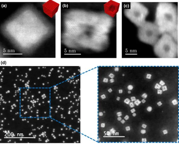
temperatures and oxidizing gas atmosphere.A high-resolution scanning TEM image of an Fe
nanocube after ambient air exposure is presented in Figure 7a, showing Fe–Fe oxide core– shell morphology, as described above. In situ thermal oxidation was performed (200°C, 1h, 20mbar O2) resulting in distinct morphological changes of Fe nanocubes: formation of voids
was observed in the NP center, as shown in Figure 7b. This phenomenon is attributed to the Kirkendall effect – a difference in solid-state diffusion rates in alloying or oxidation reactions.[64] The outward diffusion of metallic Fe is expected to be faster than the inward
oxygen diffusion, resulting in consumption of the Fe core and void formation.[65] Our environmental TEM results demonstrate that Fe NPs retain close-to-cubic shapes after complete thermal oxidation, which differs from literature results on Fe nanocubes that adopt approximately spherical shapes after long-term storage at room temperature.[66]
21
Figure 7. High-resolution scanning TEM image of Fe nanocube a) before the experiment b)
after in situ thermal oxidation (200°C, 1h, 20mbar O2) and c) after ex situ control experiment
(200°C, 1h, ambient air). d) Low magnification TEM image of Fe nanocubes after in situ
thermal oxidation and a specifically chosen area of low cubic purity (blue square).
In an ex situ control experiment shown in Figure 7c, equivalent morphological changes of Fe nanocubes were observed, validating the environmental TEM results and suggesting that the gas sensor resistance is determined by the percolation of fully oxidized, hollow Fe oxide nanocubes. We attribute the excellent sensing performance to the morphology of individual NPs: the space charge region due to chemisorbed gas species[61,67] is expected to extend to the entire Fe oxide shell, as the Debye length of undoped metal oxide semiconductors is typically in the range of few nm.[68,69] Thus the formation of hollow nanostructures ensures optimized NP morphologies for gas sensing,[70] resulting in electrical
22
conductivity being highly sensitive to minute NO2 concentrations. It is noteworthy that void
formation via the Kirkendall effect is mostly suppressed in spherical NPs under these specific conditions, as shown in Figure 7d, once more emphasizing the importance of using anisotropic NP shapes such as nanocubes. As magnetron sputtering inert-gas condensation has
been successfully employed for the synthesis of diverse nanoparticle structures,[30] it can be
applied for a broad range of materials, aiming at morphological control of gas sensing
activity.[7]
8. Conclusion
In summary, we study multifunctional Fe-based nanocubes synthesized by a simple and versatile gas-phase method. The magnetic target thickness was introduced as a crucial parameter in NP synthesis by magnetron-sputtering gas condensation, which revealed the influence of magnetic screening on Fe nanocube formation. By ensuring precise control over NP size and shape during formation instead of using mass filtration, a remarkable increase in NP deposition yield was achieved, which enabled the realization of chemoresistive gas sensor devices for NO2 detection in the low ppb-level range. The excellent sensing properties due to
specific NP morphologies combined with the inherent advantages of NP gas phase synthesis make our approach a highly promising candidate for future large-scale production of miniaturized, high-performance gas sensor devices integrated with standard microelectronic components. Furthermore, we tune the magneto-plasmonic properties by introducing dopant materials in hybrid FeAu nanocubes, which opens new prospects for biomedical applications as well as for future studies on chemoresistive sensors with improved selectivity.
23
Synthesis of Fe NPs: Fe NPs were prepared by a commercial inert-gas condensation
magnetron sputtering source. The aggregation chamber was water-cooled and the base pressure was kept below 10-6 mbar prior to sputtering. In all experiments, an Argon (Ar) flow of 55sccm was set to maintain a similar differential pressure, which dictates the residence time and temperature balance in the aggregation zone, and therefore the crystallinity and the size of the nanoparticles. Pure Fe nanoparticles were initially formed through a supersaturated vapor of metal atoms by DC sputtering of a high-purity Fe target (99.9%) under Ar atmosphere. Three different target thicknesses (1mm, 0.5mm and 0.3mm) were used to adjust the thermal environments, which determine the size and shape during formation (see main article). Due to the difference in inter-electrode distance, i.e. the distance between the target surface (cathode) and the fixed anode, for the three target thicknesses, we adjusted the DC current to balance the slight variation of the DC voltage. The aggregation length was set to 90mm and the substrate was rotated during deposition at 2 rotations per minute (rpm) to improve the uniformity.
Synthesis of FeAu NPs: FeAu NPs were obtained using a modified Fe target with two Au
pellets inserted at positions within the expected racetrack. The NPs were deposited on TEM grids and on a Polyvinylpyrrolidone (PVP) film to allow for their transfer in aqueous solution.
For the PVP film, a glass slide substrate (76mm × 26mm) was thoroughly cleaned in dry
methanol for 10min under ultra-sonication; then dried under N2 gas. 10mg of PVP
(Sigma-Aldrich, St. Louis, USA) were dissolved in 250µL of methanol solution and gently dispensed onto the clean glass substrate. A thin PVP film was formed by a spin-coater (MS-A-150, MIKASA, Japan) operated at 3,000rpm for 30sec. NPs were exfoliated by immersing the NPs/PVP/glass samples in methanol and sonicating for 15min, followed by a separation step to remove the excessive PVP polymer using a centrifuge at 100,000rpm for 60min. After
24
washing the precipitated NPs with methanol, the NPs were re-dispersed in ultrapure water from a Milli-Q system (Nihon Millipore K.K., Tokyo, Japan) using 0.1µm filters.
Materials characterization: The Fe nanoparticles were deposited on Si substrate (5 × 5mm)
and Si3N4 amorphous TEM grids (8mm film, 60 × 60m Apert. on 5 × 5mm windows) for
characterization after exposure to air. Nanoparticle dispersions on Si substrates and on gas sensing devices were analyzed using an FEI Quanta FEG 250 Scanning Electron Microscope (SEM). High Resolution Transmission Electron Microscopy (HRTEM) images were acquired using a FEI Titan 80-300kV Environmental TEM (ETEM) equipped with a Cs-image corrector and operated at 300kV and 80kV. Particle size distributions of Fe nanocubes were determined by measuring the lateral dimensions of more than 1,000 nanoparticles for each sample using low magnification TEM images. Electron Energy Loss Spectroscopy (EELS) was performed to study the native oxide formed on individual Fe nanocubes in Scanning Transmission Electron Microscopy (STEM) mode at 80kV (energy resolution of 0.2eV estimated using the full-width at half maximum (FWHM) of the zero-loss peak (ZLP) and a collection semi-angle around 13mrad). The energy loss spectra of the O K-edge and Fe L2,3
-edge were acquired simultaneously in dual EELS mode.
In-situ measurements: Environmental TEM studies were performed using a commercial TEM
heating holder based on heating chips with closed loop temperature control (Protochips Inc.). Fe nanoparticles were imaged on a carbon support in STEM mode using a high-angle annular dark-field (HAADF) detector. In situ thermal oxidation was performed with a heater setpoint temperature of 200°C for 1h at a pressure of 20mbar O2. Ex situ control experiments were
performed by heating Fe nanoparticles on Si3N4 TEM grids to 200°C for 1h in ambient air.
Supporting Information
Supporting Information is available from the Wiley Online Library or from the author.
25
Work performed at OIST was supported by funding from the Okinawa Institute of Science and Technology Graduate University. Research performed at the University of Helsinki was supported by the doctoral program MATRENA. F. Djurabekova expresses her gratitude for additional support by the Academy of Finland (Grant No. 269696).The authors are also grateful to the Finnish IT Center of Science, CSC, for grants of computational time. This work was partly supported by LAAS-CNRS micro and nanotechnologies platform member of the French RENATECH network. We thank T. Sasaki and A. J. Winchester for experimental support, Dr. J-H. Kim for the nanoparticle transfer in aqueous solution, and the Mantis R&D team for helpful discussions.
Received: ((will be filled in by the editorial staff)) Revised: ((will be filled in by the editorial staff)) Published online: ((will be filled in by the editorial staff)) References
[1] I. Lee, F. Delbecq, R. Morales, M. A. Albiter, F. Zaera, Nature Mater. 2009, 8, 132-138.
[2] K. An, G. A. Somorjai, ChemCatChem. 2012, 4, 1512-1524.
[3] S. Syrenova, C. Wadell, F. A. A. Nugroho, T. A. Gschneidtner, Y. A. D. Fernandez, G. Nalin, D. Switlik, F. Westerlund, T. J. Antosiewicz, V. P. Zhdanov, K. Moth-Poulsen, C. Langhammer, Nature Mater. 2015, 14, 1236-1244.
[4] G. Y. Tonga, K. Saha, V. M. Rotello, Adv. Mater. 2014, 26, 359-370.
[5] H. A. Atwater, A. Polman, Nature Mater. 2010, 9, 205-213.
[6] S. Linic, U. Aslam, C. Boerigter, M. Morabito, Nature Mater. 2015, 14, 567-576.
[7] A. Gurlo, Nanoscale 2011, 3, 154-165.
[8] G. Singh, H. Chan, A. Baskin, E. Gelman, N. Repnin, P. Kral, R. Klajn, Science 2014,
345, 1149-1153.
[9] Z. Nie, A. Petukhova, E. Kumacheva, Nature Nanotech. 2010, 5, 15-25.
[10] S. K. Bose, C. P. Lawrence, Z. Liu, K. S. Makarenko, R. M. J. van Damme, H. J. Broersma, W. G. van der Wiel, Nature Nanotech. 2015, 10, 1048-1052.
[11] P. D. Howes, R. Chandrawati, M. M. Stevens, Science 2014, 346, 1247390. [12] A. Tricoli, S. E. Pratsinis, Nature Nanotech. 2010, 5, 54-60.
26
[13] Y. Yan, S. C. Warren, P. Fuller, B. A. Grzybowski, Nature Nanotech. 2016, 11, 603-608.
[14] S. Steinhauer, V. Singh, C. Cassidy, C. Gspan, W. Grogger, M. Sowwan, A. Kock,
Nanotechnology 2015, 26, 175502.
[15] A. Lassesson, M. Schulze, J. van Lith, S. A. Brown, Nanotechnology 2008, 19, 015502.
[16] M. Benelmekki, M. Bohra, J-H. Kim, R. E. Diaz, J. Vernieres, P. Grammatikopoulos, M. Sowwan, Nanoscale 2014, 6, 3532-3535.
[17] G. Korotcenkov, Mater. Sci. Eng. B 2007, 139, 1-23.
[18] H.-H. Jeong, A. G. Mark, T.-C. Lee, M. Alarcon-Correa, S. Eslami, T. Qiu, J. G. Gibbs, P. Fischer, Nano Lett. 2016, 16, 4887-4894.
[19] P. Hernandez-Fernandez, F. Masini, D. N. McCarthy, C. E. Strebel, D. Friebel, D. Deiana, P. Malacrida, A. Nierhoff, A. Bodin, A. M. Wise, J. H. Nielsen, T. W. Hansen, A. Nilsson, I. E. L. Stephens, I. Chorkendorff, Nature Chem. 2014, 6, 732-738.
[20] P. R. Ellis, C. M. Brown, P. T. Bishop, J. Yin, K. Cooke, W. D. Terry, J. Liu, F. Yin, R. E. Palmer, Faraday Discuss. 2016, 188, 39-56.
[21] B. Van Issendorff, R. E. Palmer, Rev. Sci. Instrum. 1999, 70, 4497-4501. [22] S. R. Plant, L. Cao, R. E. Palmer, J. Am. Chem. Soc. 2014, 136, 7559-7562. [23] J. Zhao, E. Baibuz, J. Vernieres, P. Grammatikopoulos, V. Jansson, M. Nagel, S.
Steinhauer, M. Sowwan, A. Kuronen, K. Nordlund, F. Djurabekova, ACS Nano. 2016,
10, 4684-4694.
[24] X. Zhang, Z. Zhang, S. C. Glotzer, J. Phys. Chem. C 2007, 111, 4132-4137. [25] A.-M. Andringa, C. Piliego, I. Katsouras, P. W. M. Blom, D. M. de Leeuw, Chem.
27
[26] S. T. Navale, D. K. Bandgar, S. R. Nalage, G. D. Khuspe, M. A. Chougule, Y. D. Kolekar, S. Sen, V. B. Patil, Ceram. Int. 2013, 39, 6453-6460.
[27] D. Zhang, Z. Liu, C. Li, T. Tang, X. Liu, S. Han, B. Lei, C. Zhou, Nano Lett. 2004, 1919-1924.
[28] A. N. Abbas, B. Liu, L. Chen, Y. Ma, S. Cong, N. Aroonyadet, M. Köpf, T. Nilges, C. Zhou, ACS Nano 2015, 9, 5618-5624.
[29] H. Haberland, M. Karrais, M. Mall, Y. J. Thurner, Vac. Sci. Technol. A 1992, 10, 3266-3271.
[30] P. Grammatikopoulos, S. Steinhauer, J. Vernieres, V. Singh, M. Sowwan, Advances in
Physics: X 2016, 1, 81-100.
[31] V. Singh, C. Cassidy, P. Grammatikopoulos, F. Djurabekova, K. Nordlund, M. Sowwan, J. Phys. Chem. C 2014, 118, 13869-13875.
[32] N. Lummen, T. Kraska, Nanotechnology 2005, 16, 2870-2877.
[33] J. Li, Q-M. Chen, W. Zhang, Z-G. Li, J. J. Pan, J. Phys. D: Appl. Phys. 1996, 29, 1624-1631.
[34] M. Ganeva, A. V. Pipa, R. Hippler, Surf. Coat. Technol. 2012, 213, 41-47.
[35] S. Pratontep, S. J. Carroll, C. Xirouchaki, M. Streun, R. E. Palmer, Rev. Sci. Instrum.
2005, 76, 045103.
[36] K. Nanbu, S. Kondo, Jpn. J. Appl. Phys. 1997, 36, 4808-4814.
[37] S. Ido, M. Kashiwagi, M. Takahashi, Jpn. J. Appl. Phys. 1999, 38, 4450-4454. [38] J.-P. Wang, Proceedings of the IEEE 2008, 96, 1847-1863.
[39] P. Sigmund, Physical review 1969, 184, 383.
[40] J. Zhao, V. Singh, P. Grammatikopoulos, C. Cassidy, K. Aranishi, M. Sowwan, K. Nordlund, F. Djurabekova, Phys. Rev. B 2015, 91, 035419.
28
[42] M. A. Koten, S. A. Voeller, M. M. Patterson, J. E. Shield, J. Appl. Phys. 2016, 119, 114306.
[43] A. Shavel, B. Rodriguez-Gonzalez, M. Spasova, M. Farle, L. M. Liz-Marzan, Adv.
Funct. Mater. 2007, 17, 3870-3876.
[44] C. M. Wang, D. R. Baer, J. E. Amonette, M. H. Engelhard, Y. Qiang, J. Antony,
Nanotechnology 2007, 18, 255603.
[45] K. M. Krishnan, Ultramicroscopy 1990, 32, 309-311.
[46] J. H. Paterson, O. L. Krivanek, Ultramicroscopy 1990, 32, 319-325.
[47] V. Belotelov, I. Akimov, M. Pohl, V. Kotov, S. Kasture, A. Vengurlekar, A. V. Gopal, D. Yakovlev, A. Zvezdin, M. Bayer, Nat. Nanotechnol. 2011, 6, 370-376.
[48] D. Wang, Y. Li, Adv. Mater. 2011, 23, 1044-1060.
[49] P. Mukherjee, L. Zhou, M. J. Kramer, J. E. Shield, Appl. Phys. Lett. 2013, 102, 243103.
[50] E. A. Kwizera, E. Chaffin, X. Shen, J. Chen, Q. Zou, Z. Wu, Z. Gai, S. Bhana, R. O’Connor, L. Wang, H. Adhikari, S. R. Mishra, Y. Wang, X. Huang, J. Phys. Chem C
2016, 120, 10530-10546.
[51] H. Yu, M. Chen, P. M. Rice, S. X. Wang, R. L. White, S. Sun, Nano Lett. 2005, 5, 379-382.
[52] J. Reguera, D. J. de Aberasturi, N. Wincklemans, J. Langer, S. Bals, L. M. Liz-Marzan, Faraday Discuss. 2016, 191, 47.
[53] Y. Lee, Y. Kudryavtsev, V. Nemoshkalenko, R. Gontarz, J. Rhee, Phys. Rev. B 2003,
67, 104424.
[54] H. L. Liu, J. H. Wu, J. H. Min, Y. K. Kim, J. Appl. Phys. 2008, 103, 07D529. [55] C. de J. Fernandez, G. Mattei, E. Paz, R. L. Novak, L. Cavigli, L. Bogani, F. J.
29
[56] P. Mukherjee, P. Manchanda, P. Kumar, L. Zhou, M. J. Kramer, A. Kashyap, R. Skomski, D. Sellmyer, J. E. Shield, ACS Nano 2014, 8, 8113-9120.
[57] D. Kechrakos, K. N. Trohidou, Phys. Rev. B 1998, 58, 12169-12177.
[58] V. Amendola, M. Meneghetti, O. M. Bakr, P. Riello, S. Polizzi, D. H. Anjum, S. Fiameni, P. Arosio, T. Orlando, C.de J. Fernandez, F. Pineider, C. Sangregorio, A. Lascialfari, Nanoscale 2013, 5, 5611.
[59] S. Steinhauer, A. Chapelle, P. Menini, M. Sowwan, ACS Sens. 2016, 1, 503-507. [60] N. Dufour, A. Chapelle, F. Mesnilgrente, V. Conedera, P. Menini, 25th
Micromechanics and microsystems Europe workshop, Istanbul, Turkey (2014). [61] A. Stanoiu, S. Somacescu, J. M. Calderon-Moreno, V. S. Teodorescu, O. G. Florea, A.
Sackmann, C. E. Simion, Sens. Actuators B 2016, 213, 166-174.
[62] N. Yamazoe, K. Shimanoe, Sens. Actuators B 2008, 128, 566-573.
[63] N. Barsan, D. Koziej, U. Weimar, Sens. Actuators B 2007, 121, 18-35.
[64] Y. Yin, R. M. Rioux, C. K. Erdonmez, S. Hughes, G. A. Somorjai, A. P. Alivisatos,
Science 2004, 304, 711-714.
[65] S. Peng, S. Sun, Angew. Chem. 2007, 119, 4233-4236.
[66] A. Pratt, L. Lari, O. Hovorka, A. Shah, C. Woffinden, S. P. Tear, C. Binns, R. Kroger,
Nature Mater. 2014, 13, 26-30.
[67] N. Barsan, U. J. Weimar, Electroceram. 2001, 7, 143–167. [68] M. E. Franke, T. J. Koplin, U. Simon, Small 2006, 2, 36–50. [69] G. Rahman, O.-S. Joo, Mater. Chem. Phys. 2013, 140, 316-322. [70] J.-H. Lee, Sens. Actuators B 2009, 140, 319-336.
30
A flexible gas-phase synthesis method is demonstrated for the fabrication of multifunctional hybrid Fe nanocubes by means of morphological control during formation. Utilizing this approach, magneto-plasmonic properties of Fe nanocubes are
tailored by Au-doping and Fe-based gas sensors with remarkable performance for NO2
detection down to concentrations as low as 3 ppb.
Fe nanocubes, magnetron sputtering, gas sensor, magneto-plasmonic, molecular dynamics
Jerome Vernieres, Stephan Steinhauer, Junlei Zhao, Audrey Chapelle, Philippe Menini, Nicolas Dufour, Rosa E. Diaz, Kai Nordlund, Flyura Djurabekova, Panagiotis
Grammatikopoulos and Mukhles Sowwan*