HAL Id: hal-01710779
https://hal.archives-ouvertes.fr/hal-01710779
Submitted on 16 Feb 2018
HAL is a multi-disciplinary open access
archive for the deposit and dissemination of
sci-entific research documents, whether they are
pub-lished or not. The documents may come from
teaching and research institutions in France or
abroad, or from public or private research centers.
L’archive ouverte pluridisciplinaire HAL, est
destinée au dépôt et à la diffusion de documents
scientifiques de niveau recherche, publiés ou non,
émanant des établissements d’enseignement et de
recherche français ou étrangers, des laboratoires
publics ou privés.
Pinning force scaling of electrospun Bi-2212 nanowire
networks
Michael Koblischka, Denis Gokhfeld, Crosby Chang, Thomas Hauet, Uwe
Hartmann
To cite this version:
Michael Koblischka, Denis Gokhfeld, Crosby Chang, Thomas Hauet, Uwe Hartmann. Pinning force
scaling of electrospun Bi-2212 nanowire networks. Solid State Communications, Elsevier, 2017, 264,
pp.16-18. �10.1016/j.ssc.2017.07.002�. �hal-01710779�
Pinning force scaling of electrospun Bi-2212 nanowire networks
Michael R. Koblischka
Institute of Experimental Physics, Saarland University, Campus C 6 3, 66123 Saarbr¨ucken, Germany.
Denis Gokhfeld
Kirensky Institute of Physics, Federal Research Center KSC SB RAS, Akademgorodok 50/38, Krasnoyarsk, 660036 Russia.
Xian Lin Zeng, U. Hartmann
Institute of Experimental Physics, Saarland University, Campus C 6 3, 66123 Saarbr¨ucken, Germany.
Crosby Chang, Thomas Hauet
Institut Jean Lamour, UMR CNRS-Universit´e de Lorraine, 54506 Vandœvre-l`es-Nancy, France.
Abstract
Flux pinning forces were determined on different network samples of superconducting Bi2Sr2CaCu2O8(Bi-2212) nanowires
pre-pared by the electrospinning technique. We employed magnetization data determined by SQUID magnetometry in a wide tem-perature range 10 K < T < 35 K, where a strong superconducting signal prevails. The scaling analysis of the pinning forces was applied to interprete the data obtained. Both pure and Li-doped Bi2212 nanowire networks exhibit a peak position of h0 ∼0.11,
which is smaller than the expected value of h0= 0.2 indicating flux pinning at grain boundaries or extended defects. For the flowing
currents through such a network, the crystallographic anisotropy and the percolation play an important role, resulting in reduced peak positions as compared to bulk samples.
Keywords:
PACS:74.70.Es, 74.72.-h, 74.25.Ha
1. Introduction
Recently, superconducting nanowires of Bi2Sr2CaCu2O8
(Bi-2212) could successfully be prepared by employing the electrospinning technique [1, 2, 3]. The nanowires themselves were found to be polycrystalline, consisting of nanometer-sized grains of random orientation and exhibit diameters of about 250 nm, which is comparable to the London penetration depth, λ0. The networks of these nanowires formed by electrospinning
and the subsequent heat treatment have an extremely low den-sity and show numerous interconnects between the nanowires which enable a current flow through the entire network. The transport and magnetization measurements [2, 4] revealed that the currents can flow through the entire sample perimeter even at applied magnetic fields of 10 T. These properties of the nanowire network samples are very interesting from the under-lying physics and for possible applications. Therefore, in this letter, we analyze the flux pinning forces obtained from M(H) measurements using the model of Dew-Hughes (DH) [5, 6] to gain a deeper understanding of the magnetic behavior of the nanowire networks, which may be interesting for certain ap-plications whereever the weight of the samples counts, and we compare the resulting pinning force scaling diagrams to such of other types of Bi-2212 and Bi-2223 materials published in the
literature.
2. Experimental procedure
The Bi-2212 nanowire networks were fabricated using the electrospinning technique from an aqueous solution of polyvinylpyrrolidone (PVP, MW 1,300,000), bismuth(III)
ac-etate, strontium acetate hydrate, calcium acetate hydrate and copper(II) acetate monohydrate and followed by calcination treatment of the electrospun polymer/inorganic composite fibers including one oxygenation step in pure O2. The
chemi-cals were commercially available (Alfa Aesar GmbH & Co KG, purity above 99.99 %) and used as received without further pu-rification. X-ray analysis confirmed that the samples are pure Bi-2212 phase with some residing carbon. For the sample with Li doping, 30 x.-% Li acetate was added to the precursor solu-tion. Further details of the nanowire fabrication procedure are given elsewhere[3]. The density of our nanowire networks is found to be equal to 0.0459 g/cm3, which is considerably lower
than the theoretical density of bulk Bi-2212 (6.4 g/cm3).
The magnetization of the nanowire networks was measured using a SQUID magnetometer (Quantum Design MPMS3) with ±7 T magnetic field applied perpendicular to the sample sur-face. The onset of superconductivity takes place at 76 K, which
is somewhat lower than the bulk Tc of the Bi-2212 phase (85
K) [2, 4].
3. Results and discussion
Figure 1: (a) Optical image of heat-treated nanowire network samples. (b) SEM image (magnification 3000×) of the nanowire network after the final heat treatment.
The microstructure of the Bi-2212 nanowire networks are presented in Figs. 1 (a/b) after the final heat treatment. The nanowire networks (a) look like a thin fabric and are extremely brittle. Due to the numerous interconnects between the indi-vidual nanowires as shown in (b), transport currents can flow through the entire nanowire network sample.
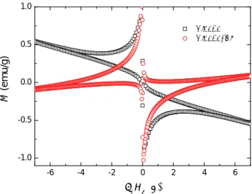
Figure 2 shows magnetization hysteresis loops of the Bi2212 and Bi2212+Li samples measured at T = 15 K. The loops ex-hibit the typical asymmetric shape of polycrystalline materials [7]. Both loops show an additional magnetic signal overlaid on the superconducting loop. For pure Bi-2212, there is a diamag-netic signal, and for the Li-doped sample, the signal is param-agnetic.
The dependence of the pinning force density on the applied magnetic field was determined by Fp(H)= µ0H × Jc(H). The
Jc(H) datapoints are obtained from the width of the
experimen-tal loops using the Bean formula. In Figs. 3, 4, the normalized
- 6 - 4 - 2 0 2 4 6 - 1 . 0 - 0 . 5 0 . 0 0 . 5 1 . 0 Bi2212 Bi2212+Li M ( e m u /g ) µ0H a (T)
Figure 2: Magnetization hysteresis loops measured at T= 15 K.
pinning force fp = Fp/Fp0 is plotted as a function of the
re-duced field h= H/Hirrfor different T, here Fp0is the maximal
pinning force density at given T . For high-Tcsuperconductors,
the values of Hirr are usually determined from a logarithmic
plot. Here we see that noise appears in the Jc(H) datapoints
right at H > Hirr. The noise level was subtracted before the
fp(h) dependencies were plotted. The resulting fp(h)
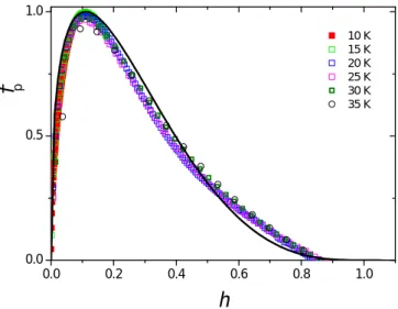
depen-dencies at all temperatures are almost coinciding, thus the fp
scaling is well developed in both types of samples studied here.
0 . 0 0 . 5 1 . 0 0 . 0 0 . 5 1 . 0 1 0 K 1 5 K 2 0 K 2 5 K 3 0 K fp h
Figure 3: Scaling of the pinning forces of the Bi2212 sample. The solid line represents the ECSM fitting curve with p= 0.37 and q = 3.
The pinning force scaling reveals a peak position, h0, of
∼0.11. This value is smaller than h0 = 0.2, which is
ex-pected for the flux pinning at 2D objects like grain boundaries [5] and was found for various Bi-based superconducting ma-terials in the literature [8, 9, 10, 11, 12, 13, 14]. This small value of h0reflects the influence of anisotropy and percolation,
which was described already in Refs. [9, 15]. The supercurrents 2
0 . 0 0 . 2 0 . 4 0 . 6 0 . 8 1 . 0 0 . 0 0 . 5 1 . 0 1 0 K 1 5 K 2 0 K 2 5 K 3 0 K 3 5 K
f
ph
Figure 4: Scaling of the pinning forces of the Bi2212+Li sample. The solid line represents the ECSM fitting curve with p= 0.37 and q = 3.
flowing within an individual nanowire have to pass grains with many different orientations, so the anisotropy factor (i.e., the anisotropy of the upper critical fields) is important to describe the resulting current. According to Ref. [15] regarding the pin-ning force analysis in bulk MgB2samples, an anisotropy factor
larger than 4, which is certainly fulfilled for Bi-2212, yields a position of h0 = 0.1 for the grain boundary pinning which
otherwise would give h0 = 0.2. The influence of percolation
effects on the peak position was found to be much smaller as described in Ref. [15]. However, the percolation effects were also found to reduce the peak positions as compared to the DH model. Therefore, one can safely conclude that the peak posi-tion h0∼ 0.1 describes grain boundary pinning in the case of an
anisotropic material and percolating currents.
For a bulk type-II superconductor with sizes much higher than the London penetration depth λ0, the dependence of the
critical current density Jc on the magnetic field H can be
ex-pressed by: Jc(H)= Jc0
1 − |H/Hc2|α
1+ |H/(h1Hc2)|α
, (1)
where α ≤ 1. This expression is a modification of the Kim-Anderson and Urban [16] dependencies. The extended criti-cal state model [17, 18, 19] supports a faster decreasing of the Jc(H) dependence due to an extension of the equilibrium
sur-face. A type-II superconductor with size being comparable to λ0has the following Jc(H) dependence:
Jc(H)= Jc0
1 − |H/Hc2|α
1+ |H/(h1Hc2)|α
(1 − |H/Hirr|)n , (2)
where n is the index defined by the geometry of the grain, n = 3 for a cylindrical sample and n= 2 for a thin plate[19].
We are interested in the behavior of the pinning force in the field range Hp < H Hc2. Given h1 1 and H Hc2, one
obtains the pinning force density from eq. (2): Fp(H) ≈ |H|1−α 1 −
|H| Hirr
!n
Jc0(h1Hc2)α . (3)
After substitution for α = 1 − p and n = q, the well-known scaling law of Dew-Hughes [5] is resulted:
fp(h)= h h0 !p 1 − h 1 − h0 !q , (4)
where h0 is the position of the maximum, h0 = p/(p + q).
The position of the pinning force maximum is easily deter-mined from graphs such that one can find the value of α from α = 1 − n/(1/h0− 1). Given h0 = 0.11 and n = 3 we obtain
α = 0.63. This corresponds to p = 0.37 and q = 3. These values differ from each other and are typical for anisotropic and polycrystalline superconductors [9, 15]. The solid line in Figs. 3, 4 represents the fp(h) dependence computed using
eq. (3) and gives a good fit to the data in both cases.
Both types of nanowire networks (undoped and doped with Li) were found to show a good scaling of the flux pinning force data, and the peak, h0 is located at ∼0.11, which is clearly
smaller than the expected value of 0.2 as found for Bi-based superconductors [8, 9, 10, 11, 12, 13, 14].
Here it should be noted that the high-h region of the Fp
-scaling plots is influenced by several factors, (i) the magne-tometer shows noise being close to its resolution, and (ii) the currents at high fields are very small and highly percolative. As a consequence, the irreversibility field is hard to determine from the plots. Nevertheless, the obtained scalung of the flux pinning forces turned out to be quite good in the temperature range in-vestigated here, and the peak position of the fp-plot is a good
indicator of the active pinning mechanism, as flux creep effects do not play a role here.
It is interesting to note that the influence of anisotropy and percolation were only recently introduced to the pinning force analysis [15], when regarding the behavior of bulk, polycrys-talline MgB2 samples. In superconducting samples with a
forced texture (bulk samples or tapes), the anisotropy does only play a minor role, and only recently, bulk, polycrystalline FeSe samples [20, 21] were found to behave similar to polycrystalline MgB2 due to a well-developed coupling between the grains.
According to Ref. [15], the changes in Fp due to changes in
the percolation threshold are comparatively small since pc is
expected to vary only between 0.2 and 0.3 in three-dimensional systems [22]. The percolation threshold mainly depends on the number of connections between the grains; thus, clean dense samples have a comparatively small pcand porous or dirty
sam-ples with a large amount of secondary phases have a larger pc.
For the present nanowire networks, the character of an individ-ual nanowire is more 2D, as only a small number of grains form the entire nanowire. This number can be as small as 3-5 grains. Furthermore, the residing carbon in the nanowire samples may be located at the grain boundaries, and this effect is even en-hanced in the case of the Li-doped samples, where we assume that Li is also found in the grain boundaries [23, 24]. Therefore, the nanowire network samples with their high porosity and the dirty grain boundaries should exhibit a stronger influence of pc
as compared to MgB2bulks analyzed in Ref. [15], which causes
a move of the peak position in the fp(h)-diagram to lower values
4. Conclusions
We have performed a pinning force scaling on the data ob-tained from electrospun Bi-2212 nanowire networks based on magnetization data. The analysis was performed using the Bean model and the ECSM model. The obtained scaling was found to quite good in the investigated temperature range 10 K < T < 35 K, and the peak position of the fp-plots were found at ∼0.11.
Due to anisotropy and percolation, this value is reduced as com-pared to the value obtained for the grain boundary pinning in bulk materials.
This work is supported by the DFG project Ko2323/8, which is gratefully acknowledged.
[1] E. A. Duarte, P. A. Quintero, M. W. Meisel, J. C. Nino, Physica C 485 (2013) 109-113.
[2] M. R. Koblischka, X. L. Zeng, T. Karwoth, T. Hauet, U. Hartmann, AIP Advances 6(2016) 035115.
[3] X. L. Zeng, M. R Koblischka, T. Karwoth, T. Hauet, U. Hartmann, Super-cond. Sci. Technol. 30(2017) 035014.
[4] M. R. Koblischka, X. L. Zeng, T. Karwoth, T. Hauet, U. Hartmann, IEEE Trans. Appl. Supercond. 26(2016) 1800605.
[5] D. Dew-Hughes, Philos. Mag. 30 (1974) 293-305.
[6] M. R. Koblischka, A.J.J. van Dalen, T. Higuchi, S. I. Yoo, M. Murakami, Phys. Rev. B 58(1998) 2863-2867.
[7] S. Senoussi, J. Phys. III France 2 (1992) 1041-1257.
[8] G. Yang, P. Shang, S. D. Sutton, I. P. Jones, J. S. Abell, C. E. Gough, Phys. Rev. B 48(1993) 40544060.
[9] P. Fabbricatore, C. Priano, A. Sciutti, G. Gemme, R. Musenich, R. Parodi, F. G¨om¨ory, J. R. Thompson, Phys. Rev. B 54 (1996) 12543-12550. [10] M. R. Koblischka, Physica C 282-287 2193-2194 (1997).
[11] S. Chu, M. E. McHenry, IEEE Trans. Appl. Supercond. 7 (1999) 1150-1153.
[12] H. Sasakura, O. Miura, D. Ito, IEEE Trans. Appl. Supercond. 9 (1999) 2332-2335.
[13] B. Ni, M. Kikuchi, E. S. Otabe, IEEE Trans. Appl. Supercond. 13 (2003) 3695-3698.
[14] M. R. Koblischka, J. Sosnowski, Eur. Phys. J. B 44 (2005) 277-280. [15] M. Eisterer, Phys. Rev. B 77 (2008) 144524.
[16] E. W. Urban, J. Appl. Phys. 42 (1971) 115-127.
[17] D. M. Gokhfeld, D. A. Balaev, M. I. Petrov, S. I. Popkov, K. A. Shaykhut-dinov, V. V. Val’kov, J. Appl. Phys. 109 (2011) 033904.
[18] D. M. Gokhfeld, Phys. Solid State 56 (2014) 2380-2386. [19] D. M. Gokhfeld, J. Phys. Conf. Ser. 695 (2016) 012008.
[20] A. Leo, G. Grimaldi, A. Guarino, F. Avitabile, A. Nigro, A. Galluzzi, D. Mancusi, M. Polichetti, S. Pace, K. Buchkov, E. Nazarova, S. Kawale, E. Bellingeri, C. Ferdeghini, Supercond. Sci. Technol. 28 (2015) 125001. [21] M. R. Koblischka, M. Muralidhar, Int. J. Mod. Phys. B 30 (2016)
1630017.
[22] S. C. van der Marck, Phys. Rev. E 55 (1997) 1514.
[23] I. Parinov, Microstructure and properties of high-Tcsuperconductors, 2nd
edition (Springer: Berlin, Heidelberg, 2012) p. 283. [24] T. B. Tang, C. R. Li, Chin. J. Phys. 36 (1998) 280-287.