HAL Id: hal-01624557
https://hal.archives-ouvertes.fr/hal-01624557
Submitted on 26 Oct 2017
HAL is a multi-disciplinary open access
archive for the deposit and dissemination of
sci-entific research documents, whether they are
pub-lished or not. The documents may come from
teaching and research institutions in France or
abroad, or from public or private research centers.
L’archive ouverte pluridisciplinaire HAL, est
destinée au dépôt et à la diffusion de documents
scientifiques de niveau recherche, publiés ou non,
émanant des établissements d’enseignement et de
recherche français ou étrangers, des laboratoires
publics ou privés.
Silicon-rich SiO2/SiO2 multilayers: A promising
material for the third generation of solar cell
F. Gourbilleau, C. Ternon, D. Maestre, Olivier Palais, C. Dufour
To cite this version:
F. Gourbilleau, C. Ternon, D. Maestre, Olivier Palais, C. Dufour. Silicon-rich SiO2/SiO2 multilayers:
A promising material for the third generation of solar cell. Journal of Applied Physics, American
Institute of Physics, 2009, 106 (1), pp.013501. �10.1063/1.3156730�. �hal-01624557�
Silicon-rich SiO
2/ SiO
2multilayers: A promising material for the third
generation of solar cell
F. Gourbilleau,1,a兲C. Ternon,1,b兲D. Maestre,2O. Palais,2and C. Dufour1
1
CIMAP, UMR CEA/CNRS/Ensicaen/Université de Caen, 6 Boulevard Maréchal Juin, 14050 Caen Cedex 4, France
2
Université-Paul Cézanne-Aix-Marseille, IM2NP, UMR CNRS 6242, Av. Escadrille Normandie Niemen, 13397 Marseille-Cedex 20, France
共Received 12 February 2009; accepted 23 May 2009; published online 1 July 2009兲
Si-rich-SiO2共SRSO兲/SiO2 multilayers 共MLs兲 have been grown by reactive magnetron sputtering. The presence of silicon nanoclusters共Si-ncls兲 within the SRSO sublayer and annealing temperature influence optical absorption as well as photoluminescence. The optimized annealing temperature has been found to be 1100 ° C, which allows the recovery of defects and thus enhances photoluminescence. Four MLs with Si-ncl size ranging from 1.5 to 8 nm have been annealed using the optimized conditions and then studied by transmission measurements. Optical absorption has been modeled so that a size effect in the linear absorption coefficient␣共in cm−1兲 has been evidenced and correlated with TEM observations. It is demonstrated that amorphous Si-ncl absorption is fourfold higher than that of crystalline Si-ncls. © 2009 American Institute of Physics.
关DOI:10.1063/1.3156730兴
I. INTRODUCTION
Since the 1950s, with the publication of a new p-n junc-tion photocell allowing the conversion of the solar radiajunc-tion into electricity, solar-electric technology made huge progress in producing efficient converters.1 The first goal was to in-crease solar cell efficiency, which was close to 5% in labo-ratory and 0.5% on commercial photocells during the 1950s. Besides, product development had to account for low cost and plentiful and nontoxic materials.
The first generation of solar cells was based on the use of mono- or polycrystalline silicon for which the main draw-back concerns its indirect optical band gap requiring a thick active layer for the solar conversion and thus sophisticated and costly procedures to fabricate large area materials.
The aim of the second generation of photovoltaic共PV兲 material was to reduce the fabrication cost through the depo-sition of thin films allowing control over the quality of the material. Apart from the Si thin film fabrication, this led to the development of Cu-based ternary semiconductors such as CdS/CuInSe2,2–4 or Cu共In,Ga兲Se2.5,6 Concerning Si-based and Cu ternary-based thin films, the literature reports conver-sion efficiencies in the 8%–26% range depending on the sub-strate and on the deposition process.7
The third generation of solar cells aims at increasing the efficiency of the PV conversion to decrease the cost per watt for producing future large scale devices.8 Such an increase can be achieved by the use of multiple energy threshold de-vices such as the well known tandem solar cell, which is constituted of individual cells able to absorb different bands of the solar spectrum.9 Thus, an all Si-based solar cell ap-proach would require the fabrication of materials in which
the Si band gap can be monitored. This has been possible since the 1990s with the discovery of the quantum confine-ment 共QC兲 effect in porous silicon leading to an intense photoluminescence 共PL兲 in the visible range at room temperature.10 Such an emission has been deeply studied in Si– SiO2 materials and ascribed to the confinement of the photogenerated carriers in Si grains whose size is smaller than 8 nm.11–14Besides the QC effect for explaining the new optical properties of nanometer-scaled Si films, some studies also pointed out the important role played by the Si/SiO2 interface in the PL.13,15–17 Thus, the PL of Si nanocluster 共Si-ncl兲 is governed by key parameters such as grain size and the Si/SiO2phase separation. An efficient absorption of light by the solar cell can be reached through the optimization of the density of Si-ncl, the Si-ncl size for a control of the absorbed wavelength of the solar spectrum, and the Si/SiO2 interface quality. Among all the fabrication techniques re-ported in the literature for providing photoluminescent Si-ncl, the most original ways to control the Si grain size are:共i兲 the laser pyrolisis of silane leading to the creation of free Si nanocrystals18 or 共ii兲 the deposition of Si/SiO2 multilayers 共MLs兲 in which the Si sublayer thickness should not exceed the critical value predicted by the QC model.19–22In addition to the control of the Si-ncl size, the ML approach offers the possibility to control the SiO2sublayer thickness, which is a key point for allowing the carrier transport through the mul-tilayered structure.
In this paper, we describe the fabrication and the optimi-zation of Si-rich silicon oxide 共SRSO兲/SiO2 MLs using a reactive magnetron sputtering approach consisting in sputter-ing a pure silica target by hydrogen-rich plasma. We inves-tigate the effects of the microstructure, the Si grain size and density, and the annealing treatment on the optical properties 共infrared absorption, PL兲.
a兲Electronic mail: [email protected].
b兲Present address: Laboratoire des Technologies de la Microélectronique 共LTM兲 Grenoble INP, CEA/LETI/D2NT, 17 Rue des Martyrs, 38 054 Grenoble Cedex 9, France.
0021-8979/2009/106共1兲/013501/7/$25.00 106, 013501-1 © 2009 American Institute of Physics [This article is copyrighted as indicated in the article. Reuse of AIP content is subject to the terms at: http://scitation.aip.org/termsconditions. Downloaded to ] IP:
II. EXPERIMENTAL
Thick SRSO/SiO2MLs have been fabricated by means of reactive magnetron sputtering. This process consists in sputtering a pure SiO2 target with hydrogen-rich plasma for incorporating Si excess in the growing layer. Depending on the deposition parameters such as hydrogen partial pressure and substrate temperature, this process allows control of Si incorporation in the grown thin film as already reported.17 For this paper, the MLs were deposited on quartz or共100兲 Si substrates maintained at 500 ° C by an alternative reactive sputtering under hydrogen-rich plasma for growing the SRSO sublayer and under pure argon plasma to obtain the SiO2 sublayer. The deposition time for these two sublayers allows control over their thickness and consequently the Si grain size within the SRSO sublayer. The power density ap-plied for the sputtering of the SiO2target was 0.76 W cm−2, whereas the hydrogen and argon partial pressures were fixed at 6.0 and 1.5 Pa, respectively. The microstructure of the MLs has been investigated through FTIR absorption spectra by means of a Nicolet 750-II spectrometer. The LO3and TO3 vibrational modes of silica at about 1250 and 1080 cm−1, respectively, are detected simultaneously by recording spec-tra at the Brewster angle of 65°. Energy filtered electron transmission microscopy 共EFTEM兲 observations have been performed using a TEM JEOL-2010 F operating at 200 kV in the cross-section and plan view configurations allowing, for the former, to observe the stacking of each sublayer in the growth direction and, for the latter, to estimate the Si nan-ograins density. For this purpose, the samples in cross sec-tion have been thinned by means of a focused ion beam technique using Ga+ ions to reduce the thickness of the samples down to 100 nm by an accurate control of the mill-ing process. For the sample in the plan view configuration, a GATAN- precision ion polishing system has been also em-ployed. The optical properties have been deduced from opti-cal transmission measurements done in the 300–2500 nm range by means of a Perkin Elmer UV-visible spectropho-tometer. Finally, the PL experiments allowing the control of the quality of the MLs were achieved using two different excitation lines, the 325 nm of HeCd laser and the 488 nm line of an Ar+laser.
III. RESULTS
A. Structure and emission properties of the
„SRSO…/SiO2multilayers
A typical TEM image of a ML produced by means of this reactive approach is displayed in Fig. 1共a兲. This image clearly shows the perfect stacking of each sublayer having a thickness of about 3 nm. The sublayer presenting the darker contrast corresponds to the SRSO sublayer in which no Si nanocrystals can be detected as evidenced in Fig. 1共b兲. One can notice the presence of a thicker SiO2sublayer thickness 共⬇5 nm兲 in contact with the Si substrate due to the presence of SiO2natural native oxide on Si substrate.
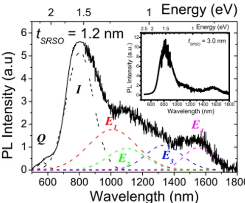
The PL emission of an annealed ML under a 325 nm HeCd laser excitation is presented in the inset of Fig.2in the 600–1800 nm range. The higher noise in the 900–1800 nm range is due to the lesser sensitivity of the Ge detector with
respect to the photomultiplier in the 550–900 nm range. One can notice the presence of a PL band peaking at about 800 nm in the visible region and two peaks 共1100–1500 nm兲 in the IR one. The suitable deconvolution for such a spectrum is achieved considering two peaks共labeled I and Q兲 in the vis-ible range, while four peaks共labeled E1to E4兲 are necessary for the IR part as evidenced for the ML with the thinnest SRSO sublayer共1.2 nm兲 共Fig.2兲. According to previous
re-sults reported in the literature,23,17 the I and Q peaks are ascribed to the electron-hole recombination 共i兲 at silicon/ silica interface for the I peak and 共ii兲 in the silicon nan-ograins within the frame of QC model for the case of the Q peak. A theoretical study24 based on these experimental re-sults has shown that both I and Q bands are superimposed on one another when some oxygen atoms are missing at the Si/SiO2interface saturated with Si= O double bonds. The E1 to E4 peaks are very close to those reported by Street in the
FIG. 1. Typical TEM images of a typical ML structure.共a兲 Bright field images showing the stacking of 3 nm thick SRSO and SiO2sublayers.共b兲 HREM images corresponding to the bright field observations in共a兲.
FIG. 2. 共Color online兲 Typical PL spectrum recorded on a 1.2 nm-SRSO/3 nm-SiO2ML after an annealing at 1100 ° C during 1 h. The inset shows the PL spectrum of a 3 nm-SRSO/3 nm-SiO2ML.
013501-2 Gourbilleau et al. J. Appl. Phys. 106, 013501共2009兲
case of the amorphous silicon.25 Consequently, their obser-vation for both SRSO sublayer thicknesses can be explained by the presence of an amorphous Si phase in the SRSO su-blayer even for tSRSO= 3 nm. This point is consistent with the work of Veprek et al.26who reported that the amorphous phase is more stable than the crystalline in Si grains whose size is smaller than 3 nm. More details on the dependence of the PL emission with tSRSOand the corresponding modeling have been reported elsewhere.17
B. Annealing treatment
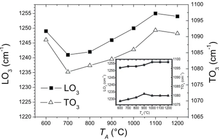
The effect of annealing temperature TA on the
600– 1100 ° C temperature range has been studied on MLs having a 3 nm thick SRSO sublayer. FTIR absorption spectra 共Fig. 3兲 show the evolution of the two main vibrational
modes, LO3and TO3, against the annealing temperature TA,
while the inset shows a typical FTIR spectrum recorded in the 900– 1400 cm−1 range. The reported values evidence that the increase in annealing temperature leads to a shift of the LO3and TO3modes to higher frequencies, from 1225 to 1255 cm−1and from 1075 to 1095 cm−1, respectively. Since a ML is dealing with silica and SRSO sublayers, this evolu-tion can be correlated with a structural rearrangement of silica or SRSO sublayers or both. To analyze the possible contribution of each sublayer, two reference samples consist-ing of a sconsist-ingle thick silica or SRSO layers were fabricated and annealed at the same temperature than the ML. In order to be comparable with the studied ML, the thickness of each film was comparable to the total thickness of all the corre-sponding sublayers共silica or SRSO兲. The evolution of their LO3and TO3modes are plotted in Fig.4for the silica single layer and in the inset共Fig.4兲 for the SRSO single film. The
comparison of these two plots for either silica or SRSO thick layers to those of Fig.3for the MLs shows some similarities such as the steep increase in the frequencies of both the LO3 and TO3modes of the ML共Fig.3兲 and the concomitant shifts of these modes in the case of a single silica layer 共Fig.4兲,
before becoming temperature independent for TAⱖ1100 °C.
Note that these modes are nearly unaffected by TA for the
single SRSO layer 共inset of Fig. 4兲. Thus, one can assume
that the evolution of the vibrational modes in the ML results
from the progressive recovering of the silica defects with TA,
which seems complete after a treatment at 1100 ° C. HREM observations共Fig.5兲 show the evolution of the
ML microstructure as a function of the annealing tempera-ture TA. These observations have shown that a TAas high as
900 ° C is required to allow the formation of Si-ncls within the SRSO sublayer, which is in agreement with previous work.20 The important role played by the interface in the control of the Si-ncl size is also evidenced since the average particle size of about 3 nm, which corresponds to the thick-ness of the SRSO sublayer, appears unaffected by the in-crease in TAuntil 1100 ° C. For TAhigher than 1100 ° C, the
Si grains grow beyond the SRSO/silica interfaces and reach a size of about 5 nm.
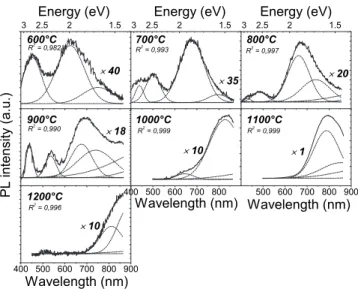
PL properties共Fig.6兲 are presented as a function of TA
in the visible range of 400–850 nm, which corresponds to the optimal working range of the photomultiplier. For each spec-trum, the corresponding fitting curves have been shown and the result of the accuracy of the fitting, R2added. Note that the intensity of these spectra does not present the same PL intensity depending on TA and has been multiplied by the
noted factor for allowing the PL comparison. These spectra show that the increasing TA up to 1100 ° C favors the PL
emission increase in the ML, beyond this maximum anneal-ing temperature, PL emission decreases. The result of the deconvolution for the ML annealed at 600 ° C evidences the presence of three emission bands peaking at 450 nm 共2.76 FIG. 3. Variation of the LO3共left scale兲 and TO3共right scale兲 phonon peaks
for a 3 nm-SRSO/3 nm-SiO2ML as a function of the annealing tempera-ture TA. The inset shows a typical infrared spectrum for TA= 1100 ° C.
FIG. 4. Evolution of the LO3共left scale兲 and TO3共right scale兲 phonon peaks with annealing temperature TAfor a thick silica layer. The inset shows the
corresponding ones recorded for a thick SRSO layer.
FIG. 5. HREM images of the MLs annealed from 900 to 1200 ° C. For the highest temperature, the arrow indicates the presence of twin boundaries appearing within the nanocrystals.
eV兲, 625 nm 共1.99 eV兲, and 750 nm 共1.65 eV兲. When TAis
increased up to 700 ° C, a fourth band appears at about 500 nm共2.48 eV兲, but for higher thermal treatment 共⬎900 °C兲, two of these bands still remain clearly observable. The same measurements have been performed on the SiO2thick single layer共spectra not shown here兲. They show the presence of a weak emission at about 630 nm共2.0 eV兲 for the lowest TA,
which disappears when this layer is annealed at high tem-perature such as 1000 ° C. The similarity with the ML PL behavior suggests that some of the bands observed with TA
can be related to the PL emission from optical transitions in the SiO2matrix, which are attributed to defects. These opti-cal transitions correspond to three spectral regions: 共i兲 from 1.85 eV 共670 nm兲 to 2.0 eV 共620 nm兲, 共ii兲 at about 2.2 eV 共564 nm兲, and 共iii兲 from 2.4 eV 共517 nm兲 to 2.8 eV 共443 nm兲.27–29
The peak positions of the emission bands obtained from the MLs共full symbols兲 and the silica layers 共open sym-bols兲 have been plotted in Fig.7as a function of the anneal-ing temperature, TA. The above-mentioned three spectral
re-gions are also indicated through the hatched areas. This graph shows that some of the PL emission bands recorded on our MLs when annealed at TA⬍1100 °C can be related to
the defects present in the silica host matrix, defects that are totally recovered for TA= 1100 ° C as evidenced with the
dis-appearance of these bands. Such notice confirms the deduc-tions made on the evolution of the FTIR spectra described above. Concerning the related interfacial and QC bands, one can notice that both bands reach their maximum intensities in layers annealed at 1100 ° C. The Q band is only affected by the annealing treatment with the occurrence of a shift toward the lower energy as well as a PL intensity decrease for the highest TAimposed. This result is correlated with the Si grain
growth and the formation of a nonrecombination site such as twin boundaries observed by HREM experiments 共Fig. 5兲.
Consequently, a thermal treatment at 1100 ° C favors the op-timum emission from Si nanocrystals and will be applied for the different MLs described hereafter.
C. Absorption of the multilayers: Effect of the Si grains size and density
Four different MLs constituted by a 1.5 nm thick SiO2 sublayer and a SRSO sublayer whose thickness tSRSO varies from 1.5 to 8 nm have been deposited on fused quartz sub-strate. Depending on tSRSO, the number of sublayers is rang-ing from 260, when tSRSO= 8 nm, to 704 for the thinnest SRSO sublayer in order to have a total film thickness of about 1.4 m for all the layers. After the optimized anneal-ing treatment at 1100 ° C duranneal-ing 1 h as described above, these films have been studied by transmission experiments and the resulting linear absorption behavior with energy
␣m共E兲 is reported on Fig. 8. Note that this coefficient has
been determined by considering the total thickness of the SRSO sublayers for each ML. One can first notice the pres-ence of oscillations on the spectra between 0.5 and 2 eV issued from reflections occurring between the film and the substrate. The analysis of the spectra evidences that the larger the grains, the higher the absorption in the whole range of energy. Considering a typical value of␣mof about
104 cm−1at 2.5 eV for mono- or polycrystalline Si used for the second generation solar cells, the comparison with our data shows that the decrease in Si-ncl size seems rather hav-ing a detrimental effect on the absorption properties of the layer. To understand why such evolution is far from the one expected, microstructural investigations by means of plan view observations and EFTEM experiments have been per-formed on the MLs with SRSO sublayers 3 nm in thickness 共Fig. 9兲. The plan view image evidences the presence of a
high density of Si nanocrystals⬇1019 cm−3 whose size is 3 nm as shown in the bottom right part of the inset 共Fig.9兲.
FIG. 6. PL spectra recorded in the 400–850 nm range of the 3 nm-SRSO/19 nm-SiO2 MLs for the indicated TA values. The scaling
factors reported on the spectra are relative to the most intense spectrum recorded after an annealing treatment at 1100 ° C.
FIG. 7. PL peaks as a function of the annealing temperature TAfor the MLs
共full symbols兲 and silica thick films 共open stars兲. The hachured areas repre-sent the emission range of silica defects.
FIG. 8. 共Color online兲 Absorption spectra of MLs for different SRSO sub-layer thicknesses.
013501-4 Gourbilleau et al. J. Appl. Phys. 106, 013501共2009兲
The corresponding filtered image acquired on the cross sec-tional view using the 16 eV Si plasmon peak is displayed in the top left-hand inset of Fig. 9. This technique allows to evidence the presence of the Si-ncls whatever their orienta-tion toward the electron beam. Thus, the embedded Si-ncls appear to be well distributed along the SRSO sublayer and are about 1.5 nm away from each other. Consequently, the value of the␣ coefficient determined above is not represen-tative of the microstructure of the SRSO sublayer and a model taking into account the spherical shape of the Si-ncls as deduced from plan view and cross-sectional observations has been done and is described hereafter.
D. Absorption model
The following model aims at establishing a relationship between the measured absorption␣min cm−1and the
absorp-tion␣grainof silicon. We assume that the absorption of silica is negligible as compared to that of silicon. We base our study on the scheme shown in Fig. 10. The incident light
strikes the sample under normal incidence with a given in-tensity I0 with a uniform flux 0. Hence I0=0SABC where
SABC is the sample surface关Fig. 10共b兲兴. We consider a part
dI0 of the light striking an elementary surface dS = 2rdr located at a radius r from the center of the grain. At this point, a photon crosses a silicon thickness of 2z共r兲 so that the output flux dI is given by the Beer Lambert law, dI = dI0e−2␣grainz共r兲=dS.
Integrating this equation over all the surfaces共ABC兲, the transmission equation can be written as
I I0 = 1 R2
冕
0 R e−2␣grainz2rdr. 共1兲Accounting for z2+ r2= R2, the r into z variable change in Eq.
共1兲 leads to I I0= 2 R2
冋
冉
− 1 2␣grainR − 1 4␣grain2冊
e −2␣grainR+ 1 4␣grain2册
. Now ␣mand␣graincan be compared from a same measure-ment of I/I0, 2 R2冋
冉
− 1 2␣grain R − 1 4␣grain2冊
e −2␣grainR+ 1 4␣grain2册
= e −2␣mR. 共2兲 We refine this model in order to account for the inter-grain space 关Fig.10共b兲兴. Let d be the distance between two grain centers. The nonabsorbing surface between the grains is Sintergrain= SABC− Sgrain=共d2冑
3/4兲−R2/2.The measured transmission can be deduced as
I I0 =
冋
冕
0 R 0e−2␣grainzrdr册
+0Sintergrain 0SABC . 共3兲Again we proceed to the same z into r variable change, we finally obtain I I0= 4 d2
冑
3冋
冉
− 1 2␣grainR − 1 4␣grain2冊
e −2␣grainR+ 1 4␣grain2册
+ 1 −R 2/2 d2冑
3 4 . 共4兲The link between␣mand␣grainis established by comparing Eq. 共4兲 and e−2␣mR. In Table Ibelow, we report the ratio of
the measured absorption共␣m兲 over the silicon absorption
co-efficient 共␣grain兲 within the grains as a function of the grain
FIG. 9. Plan view image of the ML constituted of 300 alternations of 3 nm thick SRSO sublayers and 1.5 nm thick SiO2sublayers. The insets show a HREM image of a Si nanocrystals共bottom兲 and the cross sectional view of the ML by means of EFTEM共top兲.
(b) (a)
FIG. 10.共a兲 Scheme for modeling the corrected absorption. 共b兲 Scheme for modeling the effect of the grain density: definition of the interfacial region.
TABLE I. Ratio␣m/␣grainbetween measured and pure bulk silicon absorp-tion as a funcabsorp-tion of the grain radius R and the intergrain distance d − 2R.
d − 2R共nm兲 R共nm兲 0.75 1.5 3 4 0.5 0.34 0.44 0.51 0.535 0.8 0.257 0.377 0.47 0.5 1 0.217 0.34 0.44 0.477 1.5 0.15 0.268 0.386 0.427
radius Rg and the intergrain mean distance d.
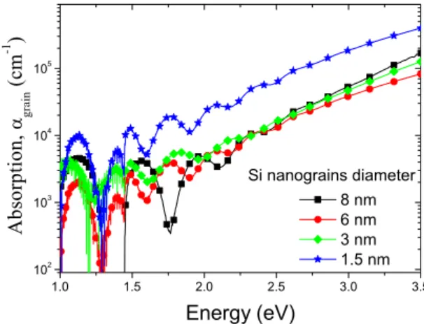
Thus, as expected, the absorption coefficient␣grainof the Si-ncl is always higher than the one 共␣m兲 deduced from the
transmission measurement. Taking into account the different nanograin radius of our MLs and fixing a mean distance d between nanograin of 1.5 nm as observed in the EFTEM images, the resulting evolution of ␣ with the energy range for different Si grain diameter is reported in Fig. 11. The curves show that the lowest Si grain size offers the highest absorption coefficient, while for diameters in the 3–8 nm range,␣is lower by a factor of 4 and the absorption curves almost similar. However, it has been previously demon-strated that the Si-ncls are amorphous below 3 nm.17Such a result means that the absorption coefficient ␣ is higher in amorphous Si-ncl by a factor of 4 in comparison with its nanocrystalline counterpart. Consequently the use of Si-ncl as structure for absorbing the solar light should take into account this properties to optimize the yield of a future cell based on Si-ncls.
E. Electrical measurements
To demonstrate the potentiality of such a structure for wide band gap front cell of tandem solar cells, the electrical behavior of a SRSO/SiO2ML has been studied by means of two probe experiments under either darkness or UV illumi-nation. For this purpose, a共3 nm-SRSO/3 nm-SiO2pattern兲 has been stacked 60 times on a p-type silicon substrate using the process described above before being submitted to an annealing treatment at 1100 ° C during 1 h under pure nitro-gen flux. Afterwards, Al dots of 1 mm in diameter have been deposited to create an Ohmic contact array with a step of 5 mm 共Fig.12兲. The I-V characteristics of the 360 nm thick
layer have been recorded under darkness 共cross兲 and UV illumination 共stars兲 as reported in Fig. 13. The comparison between the two curves shows an increase in the conductiv-ity of the device under UV illumination. To confirm the ab-sence of any effect of the substrate in the conductivity pro-cess, I-V measurements have been performed under IR illumination 共=940 nm are open circles in Fig. 13兲. The
result reported in Fig. 13 shows that the behavior of the device is similar in darkness or under IR light, which dem-onstrates that the enhancement of the conductivity observed
under UV illumination is attributed to a photoconductance effect of the nanostructured MLs. Moreover, it is worth no-ticing that the conductivity has been achieved in a “thick” mostly insulating layer and illustrates the interest of such a stacking structure in which the SiO2 sublayer thickness and the Si nanograin density can be monitored.
IV. CONCLUSION
In this paper, we investigated the optical properties 共ab-sorption and PL兲 of Si-rich SiO2/SiO2MLs fabricated using a reactive magnetron sputtering approach. The effect of the Si-ncl size, which can be easily controlled through the SRSO layer thickness, as well as the one of the annealing treatment, has been studied and analyzed. It appears that the optimized PL emission of the MLs has been obtained after an annealing as high as 1100 ° C, whereas the presence of two peaks in the visible range has been observed in the PL spectra and is attributed to the interface and the QC effect in the Si-ncl. The resulting absorption coefficient has been determined for four different Si-ncl grain sizes after applying the optimized an-nealing treatment. The EFTEM-TEM observations allowed to evidence the microstructure of the MLs and more pre-cisely the specific one of the SRSO sublayer. This has been helpful to evidence that both the Si-ncl size and density 共cluster cm−2兲 play a role on the absorption coefficient. The
I-V measurements performed on a 3 nm-SRSO/3 nm-SiO2
FIG. 11. 共Color online兲 Absorption spectra of Si-ncls for different Si-ncl diameters共2R兲.
FIG. 12. Scheme of the device structure. The active layer is constituted of 60关3 nm-SRSO/3 nm-SiO2兴 patterns.
FIG. 13. 共Color online兲 I-V measurements under darkness, IR, and UV illuminations.
013501-6 Gourbilleau et al. J. Appl. Phys. 106, 013501共2009兲
ML demonstrate a photoconductance effect under UV illumi-nation. The effect of the Si-ng size on the I-V characteristics are under progress before the realization and a test of p-n junction.
ACKNOWLEDGMENTS
Some of the authors want to thank Pr Xavier Portier for performing some of the HREM observations. This work has been supported by the ANR Solaire Photovoltaique through the DUOSIL project.
1D. M. Chapin, C. S. Fuller, and G. L. Pearson,J. Appl. Phys.25, 676 共1954兲.
2L. L. Kazmerski, M. S. Ayyagari, G. A. Sanborn, and F. R. White,J. Vac.
Sci. Technol.13, 139共1976兲.
3B. J. Brown and C. W. Bates, Jr.,J. Appl. Phys.68, 2517共1990兲. 4K. J. Hong, T. S. Jeong, and C. J. Youn, J. Appl. Phys. 100, 123518
共2006兲.
5W. K. Metzger and M. Gloeckler,J. Appl. Phys.98, 063701共2005兲. 6U. Malm and M. Edoff,Prog. Photovoltaics16, 113共2008兲.
7L. L. Kazmerski,J. Electron Spectrosc. Relat. Phenom.150, 105共2006兲. 8M. A. Green共unpublished兲.
9G. Conibeer, M. Green, R. Corkish, Y. Cho, E.-C. Cho, C.-W. Jiang, T. Fangsuwannarak, E. Pink, Y. Huang, T. Puzzer, T. Trupke, B. Richards, A. Shalav, and K.-L. Lin,Thin Solid Films511–512, 654共2006兲.
10L. T. Canham,Appl. Phys. Lett.57, 1046共1990兲.
11C. Delerue, G. Allan, and M. Lannooo,Phys. Rev. B48, 11024共1993兲. 12N. A. Hill and K. B. Whaley,Phys. Rev. Lett.75, 1130共1995兲.
13Y. Kanemitsu,Phys. Rev. B53, 13515共1996兲.
14G. Allan, C. Delerue, and M. Lannoo,Phys. Rev. Lett.76, 2961共1996兲. 15B. Garrido, M. Lopez, O. Gonzales, A. Perez-Rodriguez, J. R. Morante,
and C. Bonafos,Appl. Phys. Lett.77, 3143共2000兲.
16N. Daldosso, M. Luppi, S. Ossicini, E. Degoli, R. Magri, G. Dalba, P. Fornasini, R. Grisenti, F. Rocca, L. Pavesi, S. Bonelli, F. Priolo, C. Spinella, and F. Iacona,Phys. Rev. B68, 085327共2003兲.
17C. Ternon, C. Dufour, F. Gourbilleau, and R. Rizk,Eur. Phys. J. B41, 325 共2004兲.
18G. Ledoux, O. Guillois, D. Porterat, C. Reynaud, F. Huisken, B. Kohn, and V. Paillard,Phys. Rev. B62, 15942共2000兲.
19L. Tsybeskov, K. D. Hirshman, S. P. Dutlagupta, M. Zacharias, P. M. Fauchet, J. P. McCaffrey, and D. J. Lockwood,Appl. Phys. Lett.72, 43
共1998兲.
20M. Zacharias, J. Bläsing, P. Veit, L. Tsybeskov, K. Hirschman, and P. Fauchet,Appl. Phys. Lett.74, 2614共1999兲.
21V. Vinciguerra, G. Franzò, F. Priolo, F. Iacona, and C. Spinella,J. Appl.
Phys.87, 8165共2000兲.
22F. Gourbilleau, X. Portier, C. Ternon, P. Voivenel, R. Madelon, and R. Rizk,Appl. Phys. Lett.78, 3058共2001兲.
23Y. Kanemitsu and S. Okamoto,Phys. Rev. B56, R15561共1997兲. 24E. Degoli and S. Ossicini,Surf. Sci.470, 32共2000兲.
25R. A. Street,Adv. Phys.25, 397共1976兲.
26S. Veprek, Z. Iqbal, and F. A. Sarott,Philos. Mag. B45, 137共1982兲. 27R. Tohmon, Y. Shimogaichi, H. Mizuno, Y. Ohki, K. Nagasawa, and Y.
Hama,Phys. Rev. Lett.62, 1388共1989兲.
28S. Munekuni, T. Yamanaka, Y. Shimogaichi, R. Tohmon, Y. Ohki, K. Nagasawa, and Y. Hama,J. Appl. Phys.68, 1212共1990兲.
29H. Nishikawa, E. Watanabe, D. Ito, and Y. Ohki,Phys. Rev. Lett.72, 2101 共1994兲.