Nondestructive depth-resolved spectroscopic investigation of the heavily
intermixed In
2S
3/ Cu
„In,Ga…Se
2interface
M. Bär,1,2,兲 N. Barreau,3,兲 F. Couzinié-Devy,3S. Pookpanratana,2J. Klaer,1M. Blum,2,4 Y. Zhang,2W. Yang,5J. D. Denlinger,5H.-W. Schock,1L. Weinhardt,4J. Kessler,3 and C. Heske2,兲
1Solar Energy Research, Helmholtz-Zentrum Berlin für Materialien und Energie GmbH,
Lise-Meitner-Campus, Hahn-Meitner-Platz 1, 14109 Berlin, Germany
2Department of Chemistry, University of Nevada, Las Vegas (UNLV), Las Vegas, Nevada 89154-4003, USA 3Institut des Matériaux Jean Rouxel (IMN)-UMR 6502, Université de Nantes, CNRS, 2 rue de la
Houssinière, BP 32229, 44322 Nantes Cedex 3, France
4
Experimentelle Physik VII, Universität Würzburg, 97074 Würzburg, Germany
5
Advanced Light Source (ALS), Lawrence Berkeley National Laboratory, Berkeley, California 94720, USA
共兲
The chemical structure of the interface between a nominal In2S3buffer and a Cu共In,Ga兲Se2共CIGSe兲 thin-film solar cell absorber was investigated by soft x-ray photoelectron and emission spectroscopy. We find a heavily intermixed, complex interface structure, in which Cu diffuses into 共and Na through兲 the buffer layer, while the CIGSe absorber surface/interface region is partially sulfurized. Based on our spectroscopic analysis, a comprehensive picture of the chemical interface structure is proposed.关兴
Cu共In,Ga兲Se2 共CIGSe兲 thin-film solar cells with an n+-ZnO/i-ZnO/CdS/CIGSe/Mo/glass device structure have reached efficiencies of 20%.1To replace the CdS layer by a nontoxic, more transparent buffer, and the conventionally used chemical bath deposition by a technique allowing in-line processing, In2S3layers have been deposited by physical vapor deposition,2sputtering,3 atomic layer deposition,4and spray ion layer gas reaction.5
The In2S3/CIGSe interface has been previously investi-gated by different destructive depth-profiling techniques,2,6 high-resolution transmission electron microscopy and energy dispersive x-ray analysis,7and x-ray photoelectron spectros-copy共XPS兲.4,8,9At共post-兲deposition annealing temperatures necessary for high device efficiencies共200–250 °C兲, a pro-nounced diffusion of Cu and Na from the CIGSe/Mo/glass substrate into the nominal In2S3 buffer layer was found in these studies. However, a complete picture of the chemical interface structure is still missing. In this paper, we will re-port on the characterization of the In2S3/CIGSe interface by a combination of nondestructive techniques 关XPS and soft x-ray emission spectroscopy共XES兲兴, deliberately varying the probing depth. Our measurements result in a depth-resolved picture of the interface in unprecedented detail.
In2S3/CIGSe structures were prepared at IMN on Mo/ glass substrates.10 The absorber layers were dipped in NH3 solution 共1 M, room temperature, 1 min兲 prior to the In2S3 buffer layer deposition by thermal coevaporation of elemen-tal indium and sulfur at 200 ° C substrate temperature. To vary the In2S3 thickness, different deposition times were used. The standard 80 nm buffer used in solar cells is pre-pared in 10 min 共called “1/1” in the following兲. For refer-ence, an In2S3 layer, different In2S3: Cu standards, and a CuInS2 共CIS兲 absorber11 were deposited on Mo/glass sub-strates. After preparation, all samples were sealed in polyeth-ylene bags filled with dry N2and desiccant for transport. At
UNLV the samples were transferred into the analysis cham-ber 共base pressure ⬍5⫻10−10 mbar兲 without air exposure. XPS was performed using Mg K␣and Al K␣excitation and a Specs PHOIBOS 150 MCD electron analyzer共calibrated ac-cording to Ref.12兲. Subsequently, XES was performed at the ALS using the soft x-ray fluorescence endstation of Beam-line 8.0.
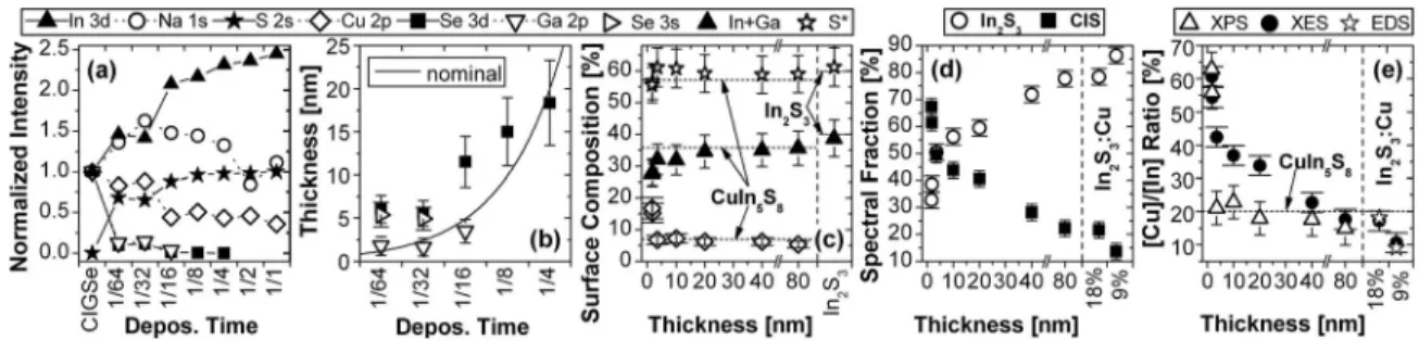
XPS survey spectra 共not shown兲 show all expected ab-sorber photoemission lines, Na-related peaks, and only minor spectral contributions of C- and O-containing surface con-taminants. The former is due to the well-known diffusion of Na from the soda-lime glass substrate through the Mo and CIGSe layers,13the latter indicates an IMN-to-UNLV sample transfer with minimal sample contamination. Upon In2S3 deposition, S-related peaks can also be observed. Further-more, the intensity of all absorber-related lines 共except In兲 decreases. However, we find significant differences in the attenuation behavior of the different CIGSe-related peaks. We have thus quantified the corresponding photoemission lines by a simultaneous fit of the spectra of all samples, using Voigt profiles and a linear background. For spin-orbit dou-blets, the respective, Gaussian and Lorentzian widths were coupled for each component and for all samples, and the intensity ratio was fixed according to the共2j+1兲 multiplicity. Figure 1共a兲 shows the intensity evolution of the different photoemission lines upon In2S3deposition, normalized to the corresponding peak intensities of the bare 共i.e., uncovered but NH3-etched兲 CIGSe absorber and the 1/1-In2S3/CIGSe sample, respectively. As expected, the intensities of the S- and In-related lines increase, while those of the Ga- and Se-related peaks decrease. In accordance with the diffusion found in Refs. 4 and 7–9, the Cu signal only decreases to approximately 40% of its initial intensity. The Na 1s inten-sity first increases and then decreases again to the same level as for the bare CIGSe surface. While the attenuation of the Se- and Ga-related peaks indicates a complete coverage of the absorber, the significant intensities for the Cu and Na signals point to a heavily intermixed interface between the In2S3 buffer and the absorber, in agreement with earlier 兲
共兲
findings8 共we will nevertheless continue to refer to the de-posited layer as In2S3 in the following兲.
The fact that the Se 3d signal decreases similarly to the Ga 2p signal is surprising, since the inelastic mean free path14 共兲 of the corresponding Se 3d photoelectrons 共⬃2.5 nm in pure In2S3 using Mg K␣ excitation兲 is signifi-cantly higher than that of the Ga 2p photoelectrons 共⬃0.5 nm兲. We have computed the corresponding effective In2S3 thickness 共d兲, assuming homogeneous and conformal absorber coverage, using I = I0⫻exp共−d/兲, where I 共I0兲 is the共un兲attenuated signal intensity. Figure1共b兲shows the dif-ferent effective thicknesses based on the attenuation of the Ga- and Se-related peaks共average of the Mg and Al K␣XPS measurements兲 in comparison with the nominal thickness. We observe that the Ga 2p-based effective thickness is 共within the error bars兲 in good agreement with the nominal thickness, while the Se 3d- and Se 3s-based effective thick-nesses are significantly increased. Only for the thickest over-layer sample with observable Se signal共the 1/4 sample兲 do we observe an agreement with the nominal thickness. This finding could be due to a partial substitution of Se by S at the absorber surface, combined with a subsequent selenium sub-limation共favored by the high selenium vapor pressure兲 in the first stages of In2S3 deposition. Although Se depletion of CIGSe surfaces due to vacuum annealing has not been re-ported for temperatures below 600 ° C,15temperatures in the range of the used substrate temperature for our In2S3 depo-sition are applied to re-evaporate Se caps from CIGSe.16 Fur-thermore, similar S/Se substitution processes have been ob-served upon CIGSe exposure to H2S atmosphere at high temperatures17 and after low-temperature chemical bath deposition of CdS.18
Note that the calculated layer thicknesses for the 1/64-and 1/32-In2S3/CIGSe samples are—within the error bars— identical. Hence, we are using the computed thickness for thin In2S3 共instead of the nominal buffer thickness兲 as the comparative parameter for the following considerations.
To quantify the XPS data, the respective peak intensities were first corrected by the corresponding 共Ref. 14兲 and photoionization cross section,19 as well as by the electron analyzer transmission. We find that both the Cu/Na and In/Na 关S/Na兴 ratios measured with Al K␣ are 共47⫾2兲%关共16⫾1兲%兴 higher than those in the more surface-sensitive Mg K␣ experiments. Our findings thus point to an accumulation of Na at all sample surfaces. The smaller
Al K␣/Mg K␣ difference for the S/Na ratio might indicate that also comparatively more S is present at the sample sur-face. We tentatively explain this with a formation of S–Na bonds at the In2S3/CIGSe sample surface. However, the pres-ence of Na in the buffer bulk can also not be excluded.
The surface composition based on the XPS signal inten-sities is shown in Fig.1共c兲as a function of In2S3thickness. Note that the S content was corrected to account for a pos-sible Na2S formation at the surface: Sⴱ=关S兴–1/2⫻关Na兴. For In2S3 thicknesses above 5 nm, the Cu:In:S composition is constant and in good agreement with a 1:5:8 stoichiometry, as indicated. This suggests a homogeneous buffer layer com-position, independent of buffer layer thickness. For verifica-tion purposes, the determined In:S composiverifica-tion 共关39:61兴%兲 of an In2S3reference layer is also shown.
To enhance bulk-sensitivity, we additionally character-ized the In2S3/CIGSe samples with the more bulk-sensitive XES. Selected S L2,3 XES spectra are shown in Fig. 2共a兲. The spectrum of the bare共S-free兲 CIGSe absorber is ascribed to the significantly less intense Se M2,3 emission 共note the magnification factor of⫻10兲. In contrast, the S L2,3emission dominates the spectra even for the thinnest In2S3 layer. Apart from the expected increase in intensity with In2S3 FIG. 1. 共a兲 Evolution of the XPS line intensities with increasing In2S3deposition time共error bars are in the range of symbol size兲. The latter is given as fraction of 10 min共the standard buffer deposition time兲. 共b兲 Comparison of the nominal thickness of the In2S3buffer with values calculated from the attenuation of different photoemission lines.共c兲 Surface composition of the investigated In2S3/CIGSe samples共as a function of buffer thickness兲 and of an In2S3reference, as computed from the measured XPS data. For comparison, the stoichiometry of a CuIn5S8and In2S3is indicated.共d兲 Spectral fractions of CIS and In2S3S L2,3XES reference spectra in the spectra of the buffer thickness series. The corresponding fractions in the S L2,3XES spectra of the In2S3: Cu standards共with nominal 9% and 18% Cu content兲 are shown for control. 共e兲 Comparison of 关Cu兴/关In兴 ratios determined from XPS and XES. For the In2S3: Cu standard samples, the EDS ratio is shown as reference共instead of the XPS ratio兲. The 关Cu兴/关In兴 ratio of a CuIn5S8compound is also indicated.
(b) XES (a) ( ) hν= 200 eV ( ) y CIS (d) [a. u .] [nm] n ten si ty CIS (d) (c) In2S3/CIGSe ten s ity 0.56 x In2S3 [ ] 1 liz e d In [nm] In t 40 80 2 3 10 nm 18% No rm a 80 1 5 10 CIGSe x 10 In2S3:Cu In2S3 0.44 x CIS N 9% 140 145 150 155 160 165 x 10 154 156 158160 162 154 156 158 160 162
Emission Energy [eV]gy [ ]
FIG. 2. 共a兲 S L2,3XES spectra of the In2S3/CIGSe samples.共b兲 Magnified valence band region, together with a CIS and In2S3reference and In2S3: Cu standards 共with nominal Cu contents of 9% and 18%, respectively兲. 共c兲 S L2,3XES valence band region of the 10 nm In2S3/CIGSe sample共open circles: raw data; gray line: fit兲 as superposition of In2S3and CIS contribu-tions. The residuum共i.e., the difference between raw data and fit兲 is shown at the bottom.共d兲 Simplified scheme of the proposed chemical structure of the surface region of a standard In2S3/CIGSe sample.
thickness, the S L2,3spectra of all In2S3/CIGSe samples look very similar at first glance. A closer look at the valence band features20 between 153 and 163 eV in Fig. 2共b兲, however, reveals significant differences between the samples. The comparison with corresponding reference spectra shows that the S L2,3spectra for thin In2S3 layers are similar to that of the CIS reference, while the S L2,3 spectrum of the thick In2S3/CIGSe samples resembles that of the In2S3: Cu stan-dards quite well.
To quantify the XES data, we used a sum of the CIS and In2S3reference spectra to共least-square兲 fit the valence band region, as exemplarily shown for the 10 nm In2S3/CIGSe sample in Fig. 2共c兲. The resulting spectral CIS and In2S3 fractions are shown in Fig.1共d兲. The CIS fraction is decreas-ing and the In2S3 fraction is increasing with In2S3 layer thickness. The quantified values confirm that the thick In2S3/CIGSe sample is very similar to the In2S3: Cu共18%兲 standard.
Assuming that the reference spectra represent stoichio-metric CIS and In2S3 samples and that the S L2,3 spectra of the In2S3/CIGSe samples can exclusively be represented as the superposition of the reference spectra, we compute a 关Cu兴/关In兴 ratio from the CIS and In2S3 fractions: 关Cu兴/关In兴=1/2⫻S L2,3共CIS兲/关1/2⫻S L2,3共CIS兲 + 2/3⫻S L2,3共In2S3兲兴. This ratio, which by design only takes into account Cu and In atoms bound to S, is shown in Fig. 1共e兲, together with the XPS-derived 共total兲 关Cu兴/关In兴 ratio. For the In2S3: Cu standards, the关Cu兴/关In兴 ratios measured by energy dispersive x-ray spectroscopy21共EDS兲 are also shown and agree very well with the XES-based ratios. For the In2S3/CIGSe samples, we find similar XPS and XES 关Cu兴/关In兴 ratios for the thinnest and thickest but not the in-termediate In2S3 layers. The expected similar values for the thick samples are in agreement with a homogeneous CuIn5S8 composition throughout the entire buffer. Since S L2,3XES spectra only probe the chemical environment of the S atoms, only the S-containing CuIn5S8 compound 关formed on a S-free 共!兲 CIGSe兴 contributes to the respective spectra. As-suming a homogeneous CuIn5S8 composition 共i.e., no Cu gradient兲, the XES 关Cu兴/关In兴 ratio of all In2S3/CIGSe samples should thus be similar to that of the formed CuIn5S8 buffer compound. The observed deviation for low thicknesses is ascribed to the substitution of Se by S in the CIGSe surface/ interface region during the first stages of the In2S3 deposi-tion, probably forming a Cu共In,Ga兲共S,Se兲2 interlayer. The difference between the XPS and XES关Cu兴/关In兴 ratios for the intermediate In2S3 thicknesses is due to the different infor-mation depths of the techniques 共more precisely: by of electrons and by the much larger attenuation length of pho-tons关here approx. 30 nm兴兲.22In the early stages of the In2S3 deposition, the buffer is thin enough such that the 共sulfur-ized兲 CIGSe side of the In2S3/CIGSe interface gives a sig-nificant contribution to both XPS and XES spectra, leading to high关Cu兴/关In兴 ratios. Then, with increasing thickness, the contribution of the In2S3/CIGSe interface region is reduced, in particular for XPS共Cu 2p⬃1 nm兲. As a result, the XPS-derived ratio rapidly decreases to the CuIn5S8 level. Due to the larger information depth the XES spectra, in contrast, still contain a substantial contribution from the interface re-gion. This results in a much slower decrease in the关Cu兴/关In兴 ratio.
The scheme in Fig.2共d兲 summarizes the findings of our XPS and XES investigation. We suggest that, during In2S3 coevaporation on a CIGSe substrate, a CuIn5S8 buffer is formed, the absorber surface/interface region is chemically modified by a partial substitution of Se by S 关probably re-sulting in a Cu共In,Ga兲共S,Se兲2interlayer兴, and Na and S ac-cumulate at the sample surface, possibly forming NaxS is-lands or a thin film. Acting as a Cu source for the CuIn5S8 formation, the CIGSe absorber near the interface will be Cu-depleted. All of these chemical “modifications” are expected to have a significant impact on the electronic structure at the interface and thus on the overall solar cell performance.
The ALS is supported by the Department of Energy, Ba-sic Energy Sciences, Contract No. DE-AC02-05CH11231.
1I. Repins, M. A. Contreras, B. Egaas, C. DeHart, J. Scharf, C. L. Perkins, B. To, and R. Noufi,Prog. Photovoltaics 16, 235共2008兲.
2N. Barreau, J. C. Bernede, S. Marsillac, C. Amory, and W. N. Shafarman,
Thin Solid Films 431–432, 326共2003兲.
3D. Hariskos, R. Menner, S. Spiering, A. Eicke, M. Powalla, K. Ellmer, M. Oertel, and B. Dimmler, Proceedings of the 19th European Photovoltaic Solar Energy Conference, Paris, France, 7–11 June 2004.
4E. B. Yousfi, B. Weinberger, F. Donsanti, P. Cowache, and D. Lincot,Thin
Solid Films 387, 29共2001兲; N. Naghavi, S. Spiering, M. Powalla, B.
Canava, and D. Lincot,Prog. Photovoltaics 11, 437共2003兲.
5N. A. Allsop, A. Schönmann, H.-J. Muffler, M. Bär, M. C. Lux-Steiner, and Ch.-H. Fischer,Prog. Photovoltaics 13, 607共2005兲.
6S. Spiering, A. Eicke, D. Hariskos, M. Powalla, N. Naghavi, and D. Lin-cot,Thin Solid Films 451–452, 562共2004兲; S. Gall, N. Barreau, S. Harel,
J. C. Bernéde, and J. Kessler,ibid. 480–481, 138共2005兲.
7D. Abou-Ras, G. Kostorz, A. Strom, H.-W. Schock, and A. N. Tiwari,J.
Appl. Phys. 98, 123512共2005兲, and references therein.
8M. Bär, N. Allsop, I. Lauermann, and Ch.-H. Fischer,Appl. Phys. Lett.
90, 132118共2007兲.
9P. Pistor, N. Allsop, W. Braun, R. Caballero, C. Camus, Ch.-H. Fischer, M. Gorgoi, A. Grimm, B. Johnson, T. Kropp, I. Lauermann, S. Lehmann, H. Mönig, S. Schorr, A. Weber, and R. Klenk,Phys. Status Solidi A 206,
1059共2009兲.
10N. Barreau, S. Marsillac, and J. C. Bernéde,Vacuum 56, 101共2000兲. 11J Klaer, J Bruns, R Henninger, K Siemer, R Klenk, K Ellmer, and D.
Bräunig,Semicond. Sci. Technol.13, 1456共1998兲, and references therein.
12C. D. Wagner, W. M. Riggs, L. E. Davis, and J. F. Moulder, in Handbook of X-Ray Photoelectron Spectroscopy, edited by G. E. Moulder 共Perkin-Elmer, Eden Prairie, 1979兲, p. 15.
13C. Heske, R. Fink, E. Umbach, W. Riedl, and F. Karg,Appl. Phys. Lett.
68, 3431共1996兲.
14S. Tanuma, C. J. Powell, and D. R. Penn,Surf. Interface Anal. 21, 165 共1994兲;QUASES-IMFP-TPP2Mcode for the calculation of the inelastic electron mean free path, Version 2.2,http://www.quases.com/.
15S. Raud and M.-A. Nicolet,Thin Solid Films 201, 361共1991兲. 16R. Hunger, T. Schulmeyer, A. Klein, W. Jaegermann, K. Sakurai, A.
Ya-mada, P. Fons, K. Matsubara, and S. Niki,Surf. Sci. 557, 263共2004兲.
17T. Nakada, H. Ohbo, T. Watanabe, H. Nakazawa, M. Matsui, and A. Kunioka,Sol. Energy Mater. Sol. Cells 49, 285共1997兲.
18C. Heske, D. Eich, R. Fink, E. Umbach, T. van Buuren, C. Bostedt, L. J. Terminello, S. Kakar, M. M. Grush, T. A. Callcott, F. J. Himpsel, D. L. Ederer, R. C. C. Perera, W. Riedl, and F. Karg,Appl. Phys. Lett.74, 1451
共1999兲; L. Weinhardt, M. Bär, S. Pookpanratana, M. Morkel, T. P. Niesen, F. Karg, K. Ramanathan, M. A. Contreras, R. Noufi, E. Umbach, and C. Heske, Appl. Phys. Lett.共to be published兲.
19J. H. Scofield,J. Electron Spectrosc. Relat. Phenom. 8, 129共1976兲. 20For a detailed discussion of the S L
2,3spectrum see, e.g., J. Reichardt, M. Bär, A. Grimm, I. Kötschau, I. Lauermann, S. Sokoll, M. C. Lux-Steiner, Ch.-H. Fischer, C. Heske, L. Weinhardt, O. Fuchs, Ch. Jung, W. Gudat, T. P. Niesen, and F. Karg,Appl. Phys. Lett. 86, 172102共2005兲.
21N. Barreau and M. Tessier, Thin-Film Compound Semiconductor Photo-voltaics, MRS Symposia Proceedings No. 1165共Materials Research Soci-ety, Pittsburgh, 2009兲, p. M08–21.
22Calculated using attenuation lengths from B. L. Henke, E. M. Gullikson, and J. C. Davis,At. Data Nucl. Data Tables54, 181共1993兲; http://www-cxro.lbl.gov/optical_constants/atten2.html.