Strain mapping at the nanoscale using precession electron diffraction in transmission electron microscope with off axis camera
Texte intégral
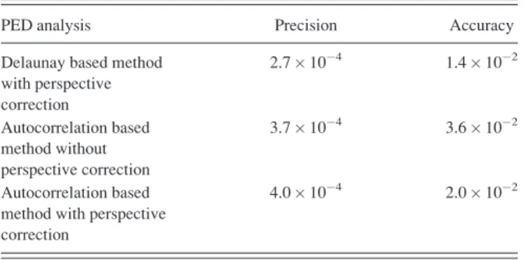
Figure
![FIG. 1. [110] PED diffraction pattern obtained in silicon (a) without and (b) with projective geometry correction](https://thumb-eu.123doks.com/thumbv2/123doknet/13436520.409296/4.918.78.446.78.449/fig-diffraction-pattern-obtained-silicon-projective-geometry-correction.webp)
Documents relatifs
For some classes of polycrystalline materials, the concepts of 3D X-ray diffraction microscopy and tomographic imaging can be merged: the combined methodology, termed X-ray
This new telescope concept allows exceptional dynamic range for photometry and high angular resolution + wide field imaging and capitalizes the exceptional atmospheric and
Monolayer condensation was explored by both LEED and Auger measurements, but the transition from an in-registry solid to a compressed, out-of-registry solid
Its two-fold b crystallographic axis coincides with the Np=x (=b) principal axis of the dielectric frame. This rotation means that generally absorption and fluorescence
These two residual measurements give us a clear indication that not only does precession reduce the ‘transfer’ of intensity between reflections within a
We have used a cross correlation based analysis of EBSD patterns to map the variation of the elastic strain tensor (and hence stress tensor) and small lattice rotations in the
In this ~vay bulk strain values have been obtained, in good agreement with values deduced from independent techniques In patterned structures, the high spatial resolution of the
A check of the validity of this zone value is then output a s a comparison of the angles measured between the chosen experimental vectors and those angles
