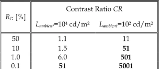
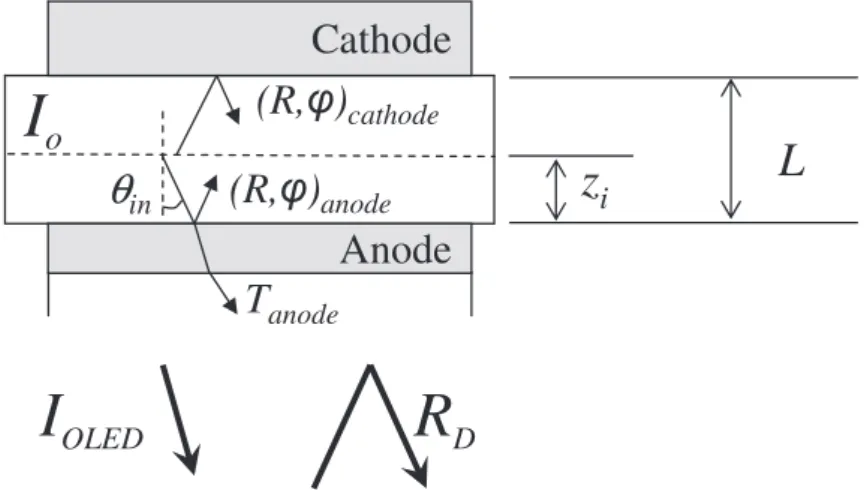
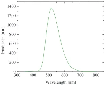
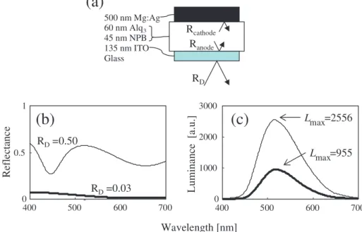
High-contrast OLEDs with high-efficiency
Texte intégral
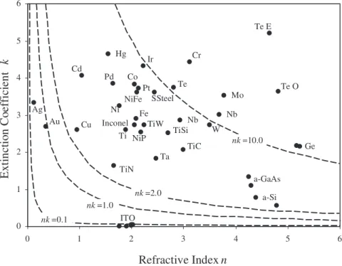
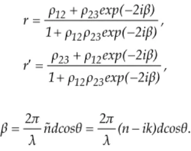
Figure


Documents relatifs
If the four compounds with three phosphorous atoms are analyzed, we can observe that NICS(1) and NICS(-1) values for 3a are more negative than expected values
Additionally, unusual events (as the 2003 heat wave or winter 1956) are likely to be recurrent. Delayed effect of extreme events may significantly reduce polycyclism frequency
The molecular composition (nanometer length scale) and polymer architecture (sub micromether length scale) of various sulfonated polymers were considered. For the discussion
Environmental impacts, in terms of greenhouse gas emissions and waste production are estimated for all activities occurring during the life cycle of both concrete deck
Four hypothetical AML patients aged 60 years or older were selected as representative of clinical practice and were summa- rized by 3 local specialists (PB, SB and
Association of serum potassium with all-cause mortality in patients with and without heart failure, chronic kidney disease, and/or diabetes.. Tamargo J, Caballero R,
L'étude conjointe de la densité, de la biomasse, de la richesse spécifique, de la diversité et de la constante m de Motomura dans 17 stations des étangs
The main leaf growth variables that we were interested in, in view of the quantitative analysis of leaf expansion at the organ, tissue and cell level, were leaf thickness,
