HAL Id: lirmm-02135043
https://hal-lirmm.ccsd.cnrs.fr/lirmm-02135043
Preprint submitted on 20 May 2019
HAL is a multi-disciplinary open access
archive for the deposit and dissemination of
sci-entific research documents, whether they are
pub-lished or not. The documents may come from
teaching and research institutions in France or
abroad, or from public or private research centers.
L’archive ouverte pluridisciplinaire HAL, est
destinée au dépôt et à la diffusion de documents
scientifiques de niveau recherche, publiés ou non,
émanant des établissements d’enseignement et de
recherche français ou étrangers, des laboratoires
publics ou privés.
Energy-Efficient HPC: an Empirical Study
Abdoulaye Gamatié, Alejandro Nocua, Joel Weloli, Gilles Sassatelli, Lionel
Torres, David Novo, Michel Robert
To cite this version:
Abdoulaye Gamatié, Alejandro Nocua, Joel Weloli, Gilles Sassatelli, Lionel Torres, et al.. Emerging
NVM Technologies in Main Memory for Energy-Efficient HPC: an Empirical Study. 2019.
�lirmm-02135043�
Emerging NVM Technologies in Main Memory for
Energy-Efficient HPC: an Empirical Study
Abdoulaye Gamati´e, Alejandro Nocua, Joel Wanza Weloli, Gilles Sassatelli,
Lionel Torres, David Novo, and Michel Robert
Abstract—The spectrum of scientific disciplines where computer-based simulation and prediction play a central role is broad: biology, medicine, high energy physics, climatology, astronomy, etc. In the near future, expected exascale supercom-puters will make it possible to address scientific problems that are more complex than ever. However, a major challenge on the path to such supercomputers is the required high energy-efficiency, i.e., maximizing the amount of computational work per watt.
To answer this challenge, the position of this paper relies on compute nodes built from inherently low-power technologies. It considers 64-bit ARM processors combined with emerging non-volatile memory (NVM) technologies for main memory, known to be a bottleneck regarding performance and energy. DRAM technology is until now the mainstream option for main memory. However, it will hardly scale beyond a certain level because increased DRAM capacity requires higher refresh rates, which is harmful to power consumption. In such a context, emerging NVMs have become promising alternatives to DRAM thanks to their memory cell density and negligible leakage. This paper eval-uates the impact of various main memory technologies, namely DDR4 SDRAM, Phase-Change Memory (PCM), Resistive RAM (RRAM), on computing system performance and memory-related energy consumption. The obtained results show that RRAM is a very promising candidate to mitigate main memory energy consumption, while PCM tends to represent a better candidate for storage level. Compared to DDR4 SDRAM, we observe RRAM can provide comparable system-level performance, while the main memory energy consumption can be reduced by up to 50%. Index Terms—Memory architecture, nonvolatile memory, phase change memory, resistive RAM, DRAM, multicore process-ing, high-performance computprocess-ing, low-power electronics, system simulation, performance evaluation
I. INTRODUCTION
E
XASCALE computing [1] is a key enabler for addressing some of the grand challenges of mankind in areas such as medicine, sustainability and climatology. Exascale is set as the next milestone in every supercomputing roadmap, albeit often postponed because of several scalability challenges among which target power consumption.Exascale computers should be capable to perform 1018
float-ing point operations per second (flops), within a reasonable power budget, typically below 20 MW. The general design challenges related to these computers concern various aspects including processor, memory and interconnect technologies,
A. Gamati´e, A. Nocua, G. Sassatelli, L. Torres, D. Novo, and M. Robert are with CNRS and University of Montpellier - LIRMM laboratory, France (e-mail: [email protected]).
J. Wanza Weloli is with Bull, Atos Technologies, France (e-mail: [email protected]).
as well as programming models. The present study focuses on compute node designs, i.e. building blocks for exascale parallel computers, based on ARM processors [2] combined with emerging non volatile memory (NVM) technologies [3]. These processors are usually energy-efficient, while emerging NVMs have inherently a negligible leakage that contributes to drastically reduce the overall power consumption in compute nodes.
A. A glance at ARM SoCs for compute nodes
ARM-based Systems-on-Chip (SoCs) are known to pro-vide a good power and performance compromise. Thanks to the generalization of 64-bit ARMv8 ISA alonside significant progress on micro-architecture and software stack, they have become attractive for high-performance computing (HPC) applications [2].
ThunderX2 processor. Among the latest solutions, we can mention the Marvell’s ThunderX2 processor, which supports ARMv8.1 architecture [4]. This chip has 8 memory channels, delivering theoretically up to 33% more memory bandwidth than its equivalent the Intel’s Skylake processor as the latter features only 6 DDR4 memory channels [5]. This translates into 33% better performance on HPCG [6] and memory-bound applications. The ThunderX2 processor has been recently compared with others x86 processors including Skylake [7]. Overall, it provides similar performance level compared to Skylake. It is slower when executing compute-bound high-performance applications due to its inherent lower floating-point throughput. In fact, it does not feature vector units contrarily to Intel Advanced Vector Extensions (AVX-512) [5]. SPARC64 XIfx processor. The A64FX CPU is the Fu-jitsu’s SPARC64 XIfx (sparc architecture) ARM-based high performance CPU successor [8]. Manufactured in 7nm pro-cess TSMC technology, it is compliant with the ARMv8.2-A specification. It is the first CPU that implements the 512-bit ARM Scalable Vector Extension (SVE), designed specifically for high performance computing [9]. It includes 48 worker cores in addition to 4 helper cores (2 I/O and 2 system) It can perform up to 2.7 teraflops for 64-bit (FP64) operations and more than 80% of the 1TB/s theoretical memory peak bandwidth delivered by four High Bandwidth Memory (HBM) blocks [9]. Floating point performance is about 35% higher than the top-of-the-line Xeon Skylake CPUs.
Kunpeng 920 processor. Recently, the Huawei’s Kunpeng 920 has been announced as the ”highest-performance ARM-based CPU” [10], exceeding A64FX. Manufactured also in
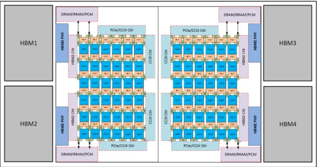
Fig. 1: A realistic ARM-based chip design
7nm, this chip integrates 64 cores at a frequency of 2.6 GHz and 8 DDR4-2933 channels. The Kunpeng 920 processor has on-board couterments including two NIC 100G RoCE for networking and a support for PCIe Gen4 and CCIX interfaces. Details about the ARM core architecture are not public yet, except the fact that the gains come from an optimization of branch prediction algorithms, a higher number of operation units, alongside an improved memory subsystem architecture. While the intrinsic compute energy-efficiency of the above ARM SoCs in terms of flops/W is very promising, the global efficiency at compute node level must also consider other crucial components such as memory. In particular, main mem-ory plays a central role regarding the efficient data access. It has a direct impact on the overall system performance and energy-efficiency. This is true in both embedded and high-performance computing domains.
EXAMPLE1 (AREALISTIC COMPUTE NODE DESIGN): The European Montblanc projects1 have been exploring the design of ARM-based supercomputers for exascale computing. A realistic compute node design in this context is shown in Figure 1. It includes ARMv8 core clusters with a three-level cache memory hierarchy, i.e. L3, L2 and L1 levels.
The corresponding SoC has 4 HBM stacks that provide up to 48GB of on-package memory. It consists of 2 dies (or chiplets) on a passive interposer, connected through high speed CCIX links and four stacks of on-chip DRAM. Additional DRAM memory controllers compatible with emerging NVM technologies are envisioned in order to improve the memory capacity. This floorplan indicates the potential of adding further IPs such as multi-channel NVM controllers, power management cores or accelerators, to exploit the silicon area of the chiplet (improving their utilization rate). However, one need to balance the trade-off of adding the new IPs, with respect to the SoC power budget.
1https://www.montblanc-project.eu
Generally, memory and I/O related macros are typically placed at the edge due to mainstream package integration technology requirements. Memory PHYs are wide structures taking significant area at the edge of the SoC. Both available edge space due to target SoC dimensions and available package pin count determine the number of memory interfaces that can be included.
B. The main memory bottleneck
A number of notable trends have been identified in the literature about main memory [11]. Modern systems keep on integrating several processing units, which can be heteroge-neous (e.g., CPUs, GPUs or FPGA) in order to fulfill the re-quirements of performance-demanding applications. Following this trend, a drop by 30% of the memory capacity per core is envisioned every two years [12]2. Therefore, per-core memory
bandwidth will decrease.
DRAM technology will further hardly scale beyond a cer-tain technology node, because of higher cell manufacturing complexity, reduced reliability, and rising cell leakage [13]. In addition, increased DRAM capacity inevitably requires higher refresh rates. The energy consumed by off-chip memory hierarchy, including DRAM, memory controller and their connecting interfaces, can reach up to 41% of the total energy consumption of a compute system [14]. In addition, the refresh mechanism of DRAM induces power consumption even when no activity occurs in the memory. For instance, authors in [15] evaluated the increase in performance and power overheads due to refresh in high-density 32Gb memory devices.
The background power consumption related to the periph-eral circuitry, e.g., word-line drivers, sense-amplifiers and write drivers, represents another concern as it contributes significantly to the memory leakage. They observed that
2To the best of our knowledge, no updated projection is provided in the
refresh can account for more than 20% of the DRAM energy consumption while running SPEC CPU2006 benchmarks with a full-system simulator. The background energy consumption is the largest part of the overall energy reported for each memory size.
DEFINITION 1 (ADDRESSEDPROBLEM): We focus on the power consumption issue of DRAM-based main memory, re-lated to their refresh and peripheral circuitry requirements. We seek cost-effective solutions that can adequately overcome this issue, without incurring neither performance penalty nor important integration efforts in compute systems.
Typically, considering the reference design shown in Figure 1, one would like to combine low-latency and high-bandwidth on-chip HBM memory with off-chip memories to extend the per core main memory capacity at least up to 2GB (required for HPC applications). In this specific case, we have to feed all cores with 128GB of main memory in total. However, we can only provide 96GB with the on-chip HBM blocs. Then, 32GB of off-chip memory are required. We have two possible choices: i) either integrate the latest DDR5 technology (DDR5-4400), or ii) integrate a custom low power and multi-channel NVM module.
C. Non volatile memory technologies
1) Making the case for NVM: To support our motivation to select NVMs as candidate solutions for the aforementioned problem, Table I introduces some numbers regarding their main characteristics [3]. We selected two very promising NVM technologies3: Resistive RAM (RRAM) and Phase Change
Memory (PCM). The table provides a relative comparison basis that will serve to assess the specific memory models used in the rest of this paper. One must keep in mind that generally at system level, the interconnect used for memory access has a notable (if not the highest) impact on those metrics. TABLE I: Approximate device-level characteristics of NVMs
DRAM Non Volatile Memory RRAM PCM Cell size (F2) 6 4 - 10 4 - 12
Read latency (nsec) ∼10 ∼10 20 - 60 Write latency (nsec) ∼10 ∼50 20 - 150
Read energy medium low medium Write energy medium high high Leakage power medium low low Write endurance > 1015 108- 1011 108 - 109
Maturity mature test chips test chips
Among the most relevant features of NVMs for energy-efficiency, we note their low leakage power. Since they are non volatile, they do not require any data refresh mecha-nism to maintain written values in the memory, contrarily to DRAM. NVMs enable to store multiple bits per cell, which leads to higher density. However, writing operation on those NVMs is more expensive compared to DRAM. Unlike charge-based memories, NVMs store data in the material structure
3Spin Transfer Torque RAM (STT-RAM) [16] is another candidate
technol-ogy, which is unconsidered in this work. In the framework of the MontBlanc3 project, it has been rather considered for the cache level hierarchy as addressed in [17], [18], and in particular at the last-level cache.
or properties (resistive switching memories). Accordingly, a write operation involves changing cell’s physical state and thus consumes more time and energy than a read operation. Furthermore, NVM cells often withstand a much smaller number of write operations before wearing out. As write endurance of NVMs is critical for most technologies, there have been significant efforts over the last years to mitigate this issue, e.g., by minimizing / avoiding memory writes via silent stores elimination [19], [20], by adopting advanced cache replacement policies [21], by applying memory mappings that account for NVM retention time [22], and by improving the technology itself [23]. Even though wear-leveling is a prominent concern for emerging NVMs, the current study will mainly focus on performance and energy concerns.
The main memory market, though extremely competitive, is a promising application area for Non-Volatile Memories (NVMs) from different perspectives:
• Technology independence: main memory comes in form
of discrete memory modules made of chips with a JEDEC DDR standardized interface, thereby lifting the difficulty of integrating different technologies on the same sub-strate.
• Voiding refresh needs: DRAM consumes a significant amount of energy into the necessary refresh cycles. The overall resulting complexity of DRAM required for cop-ing with the hierarchical organization in pages, ranks and banks incurs significant performance penalties compared to NVMs. Indeed, thanks to their inherent non-volatility, most NVMs do not require any refresh mechanism to preserve their stored data. This also confers to NVM negligible leakage.
• Scaling and density NVM memory technologies can
scale better than DRAM. For instance, the Phase-Change Memory is expected to scale to 9nm around 2022, while a 20nm prototype was already proposed in 2008 by IBM [11]. This enables denser memories that could meet the memory capacity requirements of multi/manycore compute systems.
2) A brief overview of PCM and RRAM technologies: The PCM memory technology was first proposed in 1970 [24] by Gordon Moore, co-founder of Intel. However, material quality and power consumption issues prevented commercialization of the technology until very recently. A number of indus-trial actors already announced PCM-based device prototypes (e.g., Samsung, Toshiba, IBM and SK Hynix [25]). More recently, Intel and Micron announced the 3D XPoint NVM technology [26], which shares many similarities with the PCM technology. However, details of the materials and physics of operation have not been fully disclosed. A 375GB SSD PCIe card from Intel, aimed at enterprise markets, is going to be released as the first product with this technology in 2019. Both PCM and 3D XPoint technologies are regarded as potential solutions for a compromise between main memory and storage-class memory. Their higher access latencies and dynamic power consumption compared to DRAM (see Table I) may however become penalizing at main memory level.
when Unity Semiconductor started developing its Conductive Metal-Oxide (CMOx) technology. This technology works by varying the resistance across a dielectric solid-state material. The RRAM technology has proved a promising candidate for main memory thanks to its lower power consumption and access latency compared to PCM (see Table I). It has demon-strated a good stability at 10nm node [27]. Among outstanding industrial players investing in the RRAM technology, one can mention Panasonic Semiconductor [28].
D. Our contribution
In this paper, we explore the impact of integrating emerging NVMs in ARM Compute Nodes to enable energy-efficient high-performance computing. An initial version of this work can be found in a report [29]. The proposed design analysis is achieved by adopting two simulation tools: the gem5 [30] cycle-approximate architecture simulator coupled with the NVMain main memory simulator [31].
We calibrate a DRAM model based on a Micron DDR4 datasheet [32]. We also build new PCM and RRAM memory technology models, starting from NVMain models that are further refined based on an analysis of the existing literature on NVMs. Our evaluation targets state-of-the-art heterogeneous ARMv8 multicore systems, envisioned for better processing efficiency of compute nodes in upcoming HPC systems. The explored system designs are validated on typical application workloads.
Our results show that RRAM is a very good candidate for energy issue mitigation at main memory level, while PCM would be a more promising candidate for storage level. We show that RRAM can provide system-level performance comparable to DDR4, while memory energy consumption can be reduced by up to 50%. This is not the case of PCM. E. Outline of paper.
The remainder of this paper is organized as follows: Sec-tion II presents some related work on NVM integraSec-tion at main memory level; then, Section III describes our design exploration framework; Section IV evaluates the performance and energy consumption of a compute node system model integrating different memory technologies at main memory. The aim is to confirm the relevance of NVM for energy improvement; Section V focuses on a few main memory system design choices aiming at demonstrating how the energy gains expected from NVM integration could be further im-proved; Section VI discusses some gained insights and briefly deals with the open question about the programmability of compute nodes integrating NVMs in main memory; finally, some closing remarks are given in Section VII.
II. RELATED WORK
We describe some existing studies promoting emerging NVM technology at main memory level. These studies consid-ered different main memory architectures like NVM-uniform or hybrid DRAM-NVM.
A. NVM-uniform main memory architectures
Lee et al. [33] examine the use of PCM to completely replace DRAM as main memory. They architect a PCM-based main memory system that helps mitigating the negative impact of high write energy and latency. For this purpose, they used more and smaller row buffers to improve locality and write coalescing. To address the write endurance issue, they proposed tracking and writing only modified data to the PCM device. These initial results show that performance, energy and endurance of PCM chips can be greatly improved with the proposed techniques.
In addition, one can achieve more efficient designs of NVM chips by taking advantage of the non-destructive nature of reads, which enables simpler and narrower row buffer organizations [34]. Unlike in DRAM, an entire NVM memory row does not need to be buffered by a device because reading a memory row does not destroy the data stored in the row. Meza et al. [34] showed that having narrow row buffers in emerging non-volatile devices can greatly reduce main memory dynamic energy compared to a DRAM baseline with large row sizes. This happens without greatly affecting memory endurance. And, for some NVM technologies, it can lead to improved performance.
Existing work often promote PCM and RRAM for main memory due to their smaller cell size. Nevertheless, a few studies also explored the opportunities offered by other emerg-ing NVMs such as the Spin Transfer Torque RAM (STT-RAM) [16]. For instance, Kultursay et al. [35] draw similar conclusion as Lee et al. [33] upon evaluation of the complete replacement of DRAM with STT-RAM. To tackle the long write latency and high write energy problems of STT-RAM, they proposed an architecture that selectively writes back the contents of the row buffer when it is modified. The architecture only writes back a data that is modified to reduce write operation energy and latency. In addition, to improve the locality of accesses to STT-RAM, they propose bypassing the modification of the row buffer for write operations. With the suggested modifications, the STT-RAM based main memory shows to be more energy-efficient than a DRAM-based main memory.
B. Hybrid DRAM-NVM architectures
Yoon et al. [36] make the key observation that row buffers are present in both DRAM and PCM. And, these row buffers have (or can be designed to have) the same latency and band-width in both DRAM and PCM. Yet, row buffer misses are much more costly in terms of latency, bandwidth, and energy in PCM than in DRAM. To exploit this, they devise a policy that avoids accessing in PCM data that frequently causes row buffer misses. Hardware or software can dynamically keep track of such data and allocate/cache it in DRAM while keeping data that frequently hits in row buffers in PCM. PCM also has much higher writing cost than reading cost. To take this into account, the allocation/caching policy is biased such that pages that are more likely written stay in DRAM.
Ware et al. [37] recently propose a hybrid DIMM archi-tecture combining DRAM and a modified Flash with reduced
Fig. 2: Main memory organization in NVMain-gem5 simulation flow.
read latencies. They claimed their proposal was commercially realizable. They evaluated the performance and endurance for data-center workloads. The obtained results showed that the combination can enabled 88% of the performance of a DRAM-only system of the same capacity at 23% of the cost.
Other work has examined how to reduce latency, energy, and cost of managing the metadata required to locate data in a large DRAM cache in hybrid main memories [38], [39]. Such metadata is typically stored in SRAM in traditional CPU cache architectures. In this work, Meza et al. made the observation that only a limited amount of data is accessed with high locality in a large DRAM cache and only a small amount of metadata needs to be kept to locate data in the cache. By distributing metadata within the DRAM cache itself (see [38]) and by employing their technique, the authors show similar performance to storing full cache metadata can be achieved with smaller storage size.
C. Merging main memory and storage
Emerging NVM memory technologies offer the possibility of designing systems and applications that can manipulate persistent data directly in memory, instead of going through a slow storage interface. In fact, if we keep the traditional two-level memory/storage model in the presence of these fast NVM devices as part of storage, the operating system and file system code for locating, moving, and translating persistent data from the non-volatile NVM devices to volatile DRAM becomes a great bottleneck.
Meza et al. [40] show that operating system and file system code causes most of the memory energy consumption and degrade performance by an order of magnitude in some data-intensive workloads. To avoid such overhead, they propose a persistent memory manager. It consists of a hardware ac-celeration unit that coordinates and unifies memory/storage management in a single address space that spans potentially multiple different memory technologies (DRAM, NVM, flash) via hardware/software cooperation.
Another related challenge includes the design of system resources that can concurrently handle applications/access-patterns that manipulate persistent data as well as those that manipulate non-persistent data. For example, Zhao et al. [41] address the problem of designing effective memory schedul-ing policies in the presence of these two different types of applications/access-patterns.
III. DESIGN EXPLORATION FRAMEWORK
We describe the setup of our modeling and evaluation framework. As mentioned in the introductory section, we
com-bine the gem5 and NVMain tools to carry out our design eval-uations. The gem5 simulator provides an accurate evaluation of system performance thanks to its high configurability for a fine-grained ARM architecture modeling [42] [43]. Its full-system simulation mode runs unmodified operating full-systems. It includes several predefined architecture component models, e.g., CPU, memory and interconnect. This simulator produces detailed execution statistics at the micro-architecture level. NVMain [31] is an architectural-level simulator that enables to evaluate main memory designs, as illustrated in Figure 2. It is flexible enough to allow the implementation of various memory controllers, interconnects and organizations. It is well-integrated together with the gem5 simulator, which makes it possible to simulate a variety of main memory technologies in a system. Among existing micro-architecture simulators that model NVM-based memory systems in detail, NVMain is the most advanced one to best of our knowledge. State-of-the-art simulators like DRAMSim2 [44], DRAMSys [45] and Ramulator [46] rather focus on DRAM technology modeling. It is worth-mentioning that the results presented in this paper are obtained with a full-system cycle-level simulation of the considered benchmarks and applications. This is considerably demanding in terms of simulation effort and results for most experiments in weeks of simulation on a manycore server. We believe it is necessary to gather relevant insights that fully take into account the micro-architectural features of the designed systems. Existing approaches [37] adopts reasonable simplifications by either simulating workload traces (in place of the full code) or selecting some representative portions of an application.
In the sequel, starting from the selected memory technolo-gies, we briefly describe the considered evaluated multicore heterogeneous architecture.
A. Evaluated system design
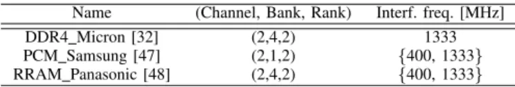
The memory models used in our study are indicated in Table II. They are designed based on a DDR4 model from Micron [32], a PCM model defined by Samsung [47] and a RRAM model defined by Panasonic [48] (see Sections III-A1 and III-A2). While the DDR4 model has been completely de-rived from the corresponding data-sheet provided by Micron, the two NVM models have been enhanced according to an in-depth review of the literature. These models are considered as inputs by NVMain to estimate delays and energy consumption of the main memory while executing various workloads.
Table II indicates for each considered memory model the number of channels, banks, ranks and interface frequencies used in our evaluations.
TABLE II: Compared 4GB main memory configurations
Name (Channel, Bank, Rank) Interf. freq. [MHz] DDR4 Micron [32] (2,4,2) 1333 PCM Samsung [47] (2,1,2) {400, 1333} RRAM Panasonic [48] (2,4,2) {400, 1333}
1) DDR4 Technology Modeling: As a reference for our study, we consider the DRAM technology used in the Cavium ThunderX2 compute nodes of the Dibona supercomputer built by Atos/Bull, within the MontBlanc 3 H2020 European project (see https://www.montblanc-project.eu/prototypes). This tech-nology consists of a DDR4 from Micron defined from the corresponding data-sheet [32]. The bandwidth of the reference memory module considered for our investigation is around 21.3GB/s according to the data-sheet.
2) NVM Technology Modeling: First of all, we note that building realistic models of PCM and RRAM technologies is not a trivial task since only a few prototype designs are currently available. The design parameters of these prototypes are hardly available. A few NVM performance and energy evaluation tools [49] [50] could be considered as an alternative solution. Unfortunately, they fail to provide the fine-grain parameter description necessary to main memory modeling. For all these reasons, we decided to rely our study on the PCM and RRAM models provided by NVMain. They respectively result from Samsung [47] and Panasonic [48] specifications, presented in the International Solid-State Circuits Conference (ISSCC’20124), the top venue for presenting the most
ad-vanced memory prototypes. While the latency parameters are consistent with the designs from Samsung and Panasonic, it is not the case of the energy parameters.
We, therefore, modified the values of energy parameters in order to get as close as possible to the featured NVMs. The detailed parameter values will be found in the appendix of our initial report [29]. We extrapolated the NVM energy parameter values according to existing literature on NVM [51] [52] [3]. In particular, we considered the following energy ratios, w.r.t. the above DDR4 model as the DRAM reference:
• 2.1x and 43.1x more energy-consuming for read and write on PCM respectively;
• 1.2x and 23.7x more energy-consuming for read and write on RRAM respectively.
On the one hand, the above ratios considered for PCM result from [51] in which authors carried out an exhaustive analysis of a number of PCM prototypes proposed in literature from 2003 to 2008. We assume these ratios remain relevant enough for the Samsung PCM model proposed in 2012 and integrated within NVMain. Note that these ratios may have been reduced today with recent advances in PCM.
4To the best of our knowledge, these are the most complete models
publically available for NVM evaluation at main memory level. In addition, the recent trends about NVMs observed in the literature suggest that the relative comparison between these technologies has not changed.
It is worth-mentioning that since 2012, state-of-the-art on NVM technologies has noticeably evolved. Therefore, the ISSCC’2012 models considered in the current study should be considered as a pessimistic approximation basis, meaning that nowadays NVM designs might enable further gains.
On the other hand, the ratios concerning the RRAM have been chosen empirically from the trends found in NVM-related literature [52] [3], which suggests that RRAM has bit-level dynamic energy that is comparable to DRAM. However, in terms of latency, writes are several times slower than reads. So, we assume that the write energy on RRAM is notably higher compared to DRAM, while it remains lower than for PCM. In fact, the recent trends about RRAM suggest that this technology has at least the same energy cost in read compared to DRAM, while the gap in write energy is getting reduced between the two technologies. Therefore, the value ratios chosen above can be seen as an upper-bound approximation that allows us to conduct a conservative analysis in the rest of this document. In other words, there exists a probable margin for improving the quantified gains reported in this work.
The maximum write bandwidths originally specified by the authors of the previous NVM models are 40MB/s for a 8Gb PCM [47] and 443MB/s for a 8Mb RRAM [48]. In the present work, an identical number of devices is used for both NVM and DDR4 models: 8 devices. Moreover, 256-bits and 512-bits row buffers are respectively considered for PCM and RRAM models. More details about the other parameters of considered memory architectures will be found in the appendix of [29]. Given this setup, we observed that the write bandwidths of the PCM and RRAM models can reach up to 400MB/s and 1500MB/s respectively, when running an application like the High Performance Conjugate Gradient (HPCCG) [6].
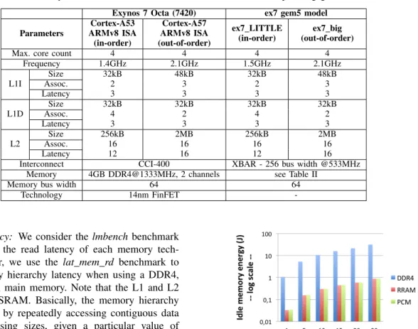
3) Heterogeneous multicore architecture: We consider the Exynos 7420 ARMv8 chip embedded in the Exsom board [53] for modeling our simulated architecture in gem5. This chip relies on the big.LITTLE technology proposed by ARM. Table III summarizes the main parameters of the architecture.
For the sake of convenience, in the remainder of this paper, we rely on the aforementioned 8-cores ARMv8 multicore architecture as a simple instance of larger scale ARMv8 high-performance compute nodes. This enables a reasonable gem5-NVMain co-simulation cost in the conducted experiments while still enabling to stress the memory subsystem. To give an idea of the overall complexity related to the experiments carried out in our current study, gem5-NVMain co-simulations have been run on a private 64 cores local server for about two months.
B. Setup validation
As a preliminary evaluation, we focus on intrinsic properties of the modeled main memories: access latency and idle power consumption. We aim at assessing the soundness of the base memory models decided in Section III.
Given the accepted relative modeling of the NVMs energy parameters (i.e. ratios w.r.t. DRAM energy) described in Section III-A2, we decided to present all our design evaluation results in the form of normalized metrics, with DDR4 as the reference for comparison. We believe absolute metric values are less relevant here. In fact, the adoption of normalized performance metrics is a standard practice in NVM-based literature for unbiased analysis [37] [33] [34] [35] [36] [40] because of the frequent relative modeling of their parameters.
TABLE III: Exynos 7 Octa (7420) SoCs characteristics and corresponding gem5 models
Exynos 7 Octa (7420) ex7 gem5 model Parameters Cortex-A53 ARMv8 ISA (in-order) Cortex-A57 ARMv8 ISA (out-of-order) ex7 LITTLE (in-order) ex7 big (out-of-order) Max. core count 4 4 4 4
Frequency 1.4GHz 2.1GHz 1.5GHz 2.1GHz L1I Size 32kB 48kB 32kB 48kB Assoc. 2 3 2 3 Latency 3 3 3 3 L1D Size 32kB 32kB 32kB 32kB Assoc. 4 2 4 2 Latency 3 3 3 3 L2 Size 256kB 2MB 256kB 2MB Assoc. 16 16 16 16 Latency 12 16 12 16 Interconnect CCI-400 XBAR - 256 bus width @533MHz
Memory 4GB DDR4@1333MHz, 2 channels see Table II Memory bus width 64 64
Technology 14nm FinFET
-1) Memory Latency: We consider the lmbench benchmark suite [54] to assess the read latency of each memory tech-nology. In particular, we use the lat mem rd benchmark to measure the memory hierarchy latency when using a DDR4, PCM and RRAM in main memory. Note that the L1 and L2 caches are both in SRAM. Basically, the memory hierarchy latency is computed by repeatedly accessing contiguous data structures of increasing sizes, given a particular value of memory stride length. In our experiments, we consider a stride length of 4kB. The result of these repetitive computations are variations in memory access latency, according to its hierarchy levels: L1 cache, L2 cache, and main memory.
Fig. 3: Memory latency with various technologies. The result provided by lat mem rd is reported in Figure 3 (here, the plotted latency values follow a logarithmic scale). The X-axis, denoted as ”Array Size”, represents the memory object sizes (in kB) for which the read latencies (in ns) are determined by the benchmark. The benchmark has been executed while using a single LITTLE core with 32kB L1 cache, 256kB L2 cache, and 4GB main memory. The memory interface frequency (i.e., the I/O bus clock) of the DDR4 memory model is 1333MHz, while the memory interface frequencies of PCM and RRAM are set to 400MHz according to the initial configuration inherited from NVMain original
Fig. 4: Idle memory energy consumption.
setup.
As expected, Micron’s DDR4 model offers a better memory latency compared to both RRAM and PCM. Their respective main memory latencies are nearby 69 nsec, 383 nsec, and 813 nsec. In other words, read accesses in the considered DDR4 model are respectively 5.5 and 11.7 times faster in comparison with RRAM and PCM respectively.
Comparing these results w.r.t. the tendencies usually found in the literature (see Table I), we observe that the device-level slowdown of PCM in read latency compared to RRAM and DRAM is confirmed. However, this is not the case for RRAM compared to DRAM: while the read latencies of the two memory technologies are similar at device level, it is not the case at memory system level. Indeed, read accesses with DDR4 are faster than with RRAM.
2) Idle Memory Power Consumption: An substantial ad-vantage of NVMs is that they do not require any data refresh mechanism thanks to their non-volatile nature. It is not the case of DRAM, which can consume a non-negligible amount of energy due to refresh process and background power. The refresh process periodically reads data from a memory area and immediately rewrites the data to the same area, while the background power is due to the peripheral logic.
Given the anticipated significance of the refresh and back-ground energy consumption for DRAM, we assess its impact compared to the considered RRAM and PCM memory models. For this purpose, we evaluate several scenarios with
little-to-no access in main memory, i.e., little-to-no read, little-to-no write. In Figure 4, we report the energy of a quasi-idle 4GB main memory for modified durations, varying from 1 second to 30 seconds. This is achieved in gem5 by executing the ”sleep” system call with different input delay values in seconds. The reported values enable us to analyze the impact of the overhead related to the background power and the refresh mechanism on the DDR4 memory energy consumption.
The total energy consumption computed by NVMain con-sists of the sum of four components: background energy, refresh energy, activate energy and burst energy. These param-eters are automatically produced among the output statistics of NVMain after each simulation. This enables a fine-grain analysis of the energy breakdown. In all experiments shown in Figure 4, we observe that with the DDR4 the energy consumption of the main memory grows significantly with bigger input delays, due to the background and refresh energy components (negligible in NVMs). On the contrary, only a marginal energy increase is observed with RRAM and PCM. This shows the potential energy saving opportunity offered by NVMs for execution scenarios where the main memory is under-used. NVMain essentially provides two device-level energy models: current-mode and energy-mode [31]. Each mode relies on a specific power estimation strategy. The current-mode uses IDD values for power calculation (as in standard DRAM simulators) and applies to DRAM systems. The energy-mode exploits energy estimations resulting from circuit-level simulators like NVSim [49] or CACTI [55]. Each memory operation increments the system energy usage, while standby and powerdown energies are computed from simulated leakage values. In our experiments, the current-mode is used for DDR4. The energy-mode is selected for the two NVM models.
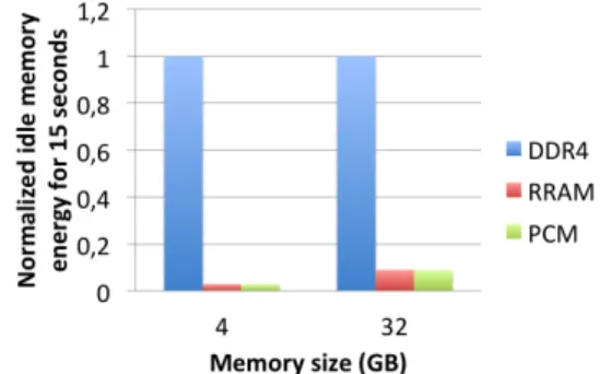
Fig. 5: Idle main memory energy: 4GB versus 32GB When increasing the size of the main memory, NVMs further mitigate energy consumption. This is illustrated in Figure 5, where the size of the main memory is increased from 4GB to 32GB while keeping unchanged the other memory parameters. The reported results concern an execution of the ”sleep” system call for 15 seconds.
The above preliminary evaluation of the NVM models regarding their latency and energy consumption is in line with the existing observation from literature: refresh and background energy consumption has an important impact on the global energy consumption of advanced DRAM-based memories [15]. This suggests the considered PCM and RRAM
models are relevant enough to be used for further investiga-tions.
In particular, provided these results, we can quantify the latency gap between the considered NVM technologies w.r.t. a typical DDR4 model when integrated into main memory. Note that the read latencies have been determined by using a benchmark designed for this specific purpose within the stream benchmark set. It will be interesting to evaluate the impact of NVMs application-wise.
IV. ASSESSMENT ON TYPICAL APPLICATIONS
We consider the Parsec benchmark set for evaluating the impact of the PCM and RRAM models, compared to the Micron DDR4 model, within a 4GB main memory model. The applications provided within Parsec provide evaluation scenarios that are more representative of applications. A. Evaluation Parsec benchmarks
1) Selected benchmarks: For the sake of simplicity, we consider three categories of applications, each featured by one representative workload from Parsec: blackscholes, dedup and swaptions. The dedup workload is mainly memory-bound benchmark, particularly with a high number of read transac-tions in the memory. It is dedicated to the definition of high data stream compression ratios. The blackscholes workload is mainly compute-intensive, with marginal memory accesses compared to the two others. It expresses an analytical price calculation based on the Black-Scholes partial differential equation. Finally, the swaptions workload shows intermediate memory access properties compared to the previous two. It applies Monte Carlo simulation to compute prices.
These workloads are selected based on a previous charac-terization described in [56]. Their corresponding properties in terms of memory access and computation load are summa-rized in Table IV. The reported values denote in billion the number of floating-point operations (FLOPs), read and write instructions.
In the rest of the document, we, therefore, consider blacksc-holes, dedup, and swaptions as the respective representatives of low memory access, high memory access, and moderate memory access applications.
TABLE IV: Breakdown of benchmark in billion instructions [56] Benchmarks 109 FLOPs 109 Reads 109 Writes blackscholes 1.14 0.68 0.19 dedup 0 11.71 3.13 swaptions 2.62 5.08 1.16
To confirm the memory access properties of the above three workloads with medium input sets5, we run them by consid-ering the same system setup as described in Section III-B1. The resulting profiles in terms of read and write bandwidths
5The breakdown shown in Table IV considers large input sets run on a real
computer. At this point, it is utilized as an initial criterion for benchmarks selection w.r.t. their characteristics. In our experiments, we use rather medium input sets because it is more tractable with gem5 in term of simulation time.
(a) blackscholes (low memory accesses)
(b) dedup (high memory access)
(c) swaptions (medium memory access)
Fig. 6: DDR4 Read/Write bandwidth for 3 benchmarks
for each of the workloads are illustrated in Figure 6. They are compliant with the read/write volumes characterized in [56]. Indeed the read/write bandwidth thresholds obtained with dedup and swaptions globally dominate that of blackscholes since they perform more memory accesses than blackscholes. This is distinctly visible for dedup, which has the highest memory activity in terms of both read and write transactions, among the three benchmarks.
We notice that only a small fraction of the memory band-width is used by the three benchmarks (i.e., far from memory bandwidth saturation, which is around 21.3GB/s according to the reference data-sheet [32]).
2) Evaluation results: Now, let us consider the execution of the three workloads by varying the memory technology in
main memory as in the previous section, i.e., DDR4, RRAM, and PCM. Medium input sets are used for the experiments. Figure 7 reports the different results. More precisely, the execution time and the main memory energy consumption are illustrated.
On the one hand, in Figure 7a, we observe that the maximum execution slowdown between DDR4 and PCM is about 7.2x. Between DDR4 and RRAM it is only about 1.7x. These slowdown factors of NVMs over DDR4 are obtained with the dedup memory-intensive workload. The high write-induced cost of NVMs, especially with PCM, exacerbates the slowdown compared to DDR4 as observed with dedup which contains more writes. Nonetheless, we can interestingly observe the above slowdown factors of NVMs are respectively smaller than the previous 11.7x and 5.5x memory latency gap obtained with the lat-mem rd benchmark (see Figure 3). This suggests that the detrimental impact of the intrinsic higher memory latencies of NVMs compared to DRAM, is limited application-wise on corresponding execution times, even for a memory-intensive workload. For application workloads with low and moderate memory accesses, the slowdown ratios between DDR4 and NVM based scenarios are further reduced. It is the case of blackscholes and swaptions in Figure 7a.
The important overhead in execution time observed for dedupand swaptions, while using PCM in main memory, is mostly due to the write transactions. Since write latency with PCM is higher than with RRAM (see Table I), this exacerbates the gap between the execution times resulting in the two NVM technologies. The overhead in execution time observed for the swaptions workload compared to the blackscholes workload mainly comes from the higher number of read transactions in the former. For yet undetermined reason we observe that for the blackscholes workload, the PCM model unexpectedly yields a faster execution time compared to RRAM. A possible explanation lies in the cache replacement policy that for this particular benchmark may be counter-productive, performing (unadequate) replacements faster with DDR4 and RRAM that in turn result in higher cache miss rate.
On the other hand, the energy consumption of the main memory with NVMs is always smaller than with DDR4, no matter the workload type (see Figure 7b). Of course, the energy gap observed application-wise is more important than with the ”Idle Memory” scenario described formerly in Figure 4, due to the dynamic activity of the memory. To appreciate the global benefit of NVM integration in main memory, let us consider the Energy-Delay-Product (EDP) from the main memory perspective only. The EDP is calculated as the product of the workload execution time and the energy consumed by the main memory during the execution time. The aim is to assess the global benefit of each design alternative. Figure 7c shows the normalized EDP of all memory configurations, according to the three representative workloads. One can see that NVMs always provide better EDP than DDR4, except for one scenario: when dedup is executed while the main memory is in PCM. In other words, for memory-intensive applications, the energy reduction enabled by the PCM technology cannot be compensated by its higher device-level read/write latencies.
(a) Normalized system executime time (b) Normalized memory energy consumption (c) Normalized memory EDP
Fig. 7: System execution time, energy consumption and Energy-Delay-Product of main memory with DDR4 and RRAM and PCM (smaller execution time, energy consumption and EDP are better)
B. Evaluation on Typical HPC workloads
1) Memory-bound benchmarks: We further evaluate NVM integration in main memory by considering the so-called MontBlanc benchmarks [57], which are representative of HPC workloads. We select four memory-bound benchmarks that feature various memory accesses and computational require-ments. The 3D Stencil (3dstc) benchmark, which takes as input a 3D volume and produces an output 3D volume of the identical size. It is a memory-bound benchmark that features stridden memory accesses. The N-Body (nbody) benchmark requires a number of input parameters including a number of bodies including their position, mass, and initial velocity. Next, it updates these parameters based on gravitational interference between bodies. It features irregular memory accesses. The Sparse Vector-Matrix Multiplication(spvm) computes a vector resulting from the product of its input vector and sparse matrix. It features computational behaviors with potential load imbalance. Finally, Vector Operation (vecop) computes a vector resulting from an element-wise addition of two input vectors. It captures intensive regular computational behaviors. Note that vector-matrix multiplication and vector addition are memory-bound algorithms [58].
(a) Normalized system exectution time
(b) Normalized memory energy consumption
Fig. 8: Normalized exec. time and main memory energy of selected Montblanc benchmarks [57]
The execution time and memory energy consumption ob-tained when executing the above HPC benchmarks are shown in Figure 8. Here, an interesting insight concerns the main memory energy consumption. Unlike with dedup which has many memory accesses, NVMs lead to worse global memory energy consumption with the 3dstc and vecop benchmarks. However, for the n-body and spvm benchmarks, NVMs and especially RRAM, significantly improve memory energy con-sumption, so that the corresponding EDP remains better than that obtained with DDR4.
The above results motivate the need of design solutions such as hybrid DRAM-NVM main memory designs (see Section II). Such designs are capable of adjusting the choice of the suitable memory target according to the energy outcome of given memory-bound workloads. This will enable to mitigate the energy penalty.
2) Representative mini-applications: Now, we evaluate the impact of designed system models on two HPC mini-applications that can be simulated in a reasonable time.
The Livermore Unstructured Lagrangian Explicit Shock Hy-drodynamics (Lulesh) mini-application [59] encodes a discrete approximation of the hydrodynamics equations. It partitions the spatial problem domain into a collection of volumetric elements defined by a mesh. It presents high instruction-level and memory-instruction-level parallelism with bursts of independent memory accesses. We consider its implementation in OpenMP. The High-Performance Conjugate Gradient (HPCG) mini-application [6] for a 3D chimney domain on an arbitrary number of processors. It has been devised with the aim of providing a metric for assessing HPC systems. It enables to exercise computational and data access patterns, which feature a range of applications. HPCG shares a similar goal as the popular High-Performance LINPACK (HPL) benchmark [60]. The HPCCG 1.0 OpenMP implementation is considered in the evaluation presented below. It includes three main computation kernels called waxpby (sum of two scaled vectors), ddot (dot product of two vectors) and sparsemv (sparse matrix vector product). Its three input parameters nx, ny and nz denote the number of nodes in the 3D dimensional domain. Here, it will be executed on 8-cores big.LITTLE architecture.
Analysis of execution outputs. The output corresponding to 8-threads execution of Lulesh with the previous three main memory configurations (DDR4, RRAM, and PCM) is
summarized in Table V. The main performance measurements reported by the Lulesh application are summarized. Elapsed time denotes how much time it takes to perform the simulation. Grind time denotes the time it takes to update a single zone for one iteration of the time-step loop. Lower values of this measure mean better performance. The Lulesh Figure-Of-Merit (FOM) provides the number of updated zones per second. These results are obtained by considering as inputs: a problem size of 153 per domain until completion, while the total number of elements is 3375.
TABLE V: Lulesh execution statistics w.r.t. selected memory technologies
DDR4 RRAM PCM Elapsed time (s) 2.54 2.51 6.04 Grind time (µs / z / c) 1.88 1.86 A.47 FOM (z / s) 531.08 536.82 223.45
The performance numbers obtained upon executing HPCCG with three main memory configurations are summarized in Ta-ble VI. As expected, the configuration with DDR4 provides the best performance in terms of mega floating point operations per second (MFLOPS). The performance degradation induced by RRAM is very limited compared to PCM. This is due to their respective high memory access latencies. These results, obtained after 149 iterations, correspond to a parallel execution of 8 OpenMP threads, where the input parameters (nx, ny, nz) equal (104, 104, 104).
TABLE VI: HPCCG execution statistics w.r.t. selected mem-ory technologies DDR4 RRAM PCM Time (s) DDOT 3.67 4.72 14.08 WAXPBY 14.94 11.48 70.34 SPARSEMV 41.27 59.78 218.28 Total 59.95 76.04 302.82 Performance (MFLOPS) DDOT 182.37 141.79 47.60 WAXPBY 67.31 87.56 14.29 SPARSEMV 219.27 151.39 41.46 Total 178.91 141.05 35.42
From these results, the DDR4 and RRAM configurations lead to almost similar performance results with respectively 531.08 and 536.82 z/s FOM values (RRAM even slightly outperforms DDR4). They are far better than with the PCM configuration, which has penalizing memory access latency.
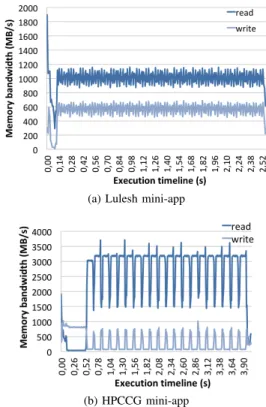
Analysis of memory activity. We focus on the main memory activity for the previous two mini-applications in order to analyze the implication of the different memory technologies w.r.t. the performance results described above. Figure 9 presents the main memory read/write bandwidths for the various technologies.
Overall, the Lulesh mini-application exhibits lower band-width thresholds (both for read and write) than HPCCG. Therefore, the performance penalty is expected to be more visible with the latter. This explains why the gap in execution times between DDR4 configuration and NVM configurations is more important for HPCCG, e.g., more than four times when comparing DDR4 and PCM (see Figure 10b). This gap
(a) Lulesh mini-app
(b) HPCCG mini-app
Fig. 9: Main memory Read/Write bandwidth for DDR4
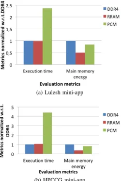
remains below 2.5x for these technologies when considering Lulesh (see Figure 10a). Note that for both mini-applications, the RRAM technology provides comparable execution time than DDR4.
The main memory energy consumption shown in Figure 10 for both mini-applications shows that NVMs always provide improvements compared DDR4, despite their possible perfor-mance penalty. Nevertheless, when considering the Energy-Delay-Product (EDP) figure-of-merit, PCM never appears as efficient as DDR4 because of the high performance degrada-tion it induces. This is not the case of RRAM, which provides a better EDP than the DDR4 configuration, whatever the mini-application.
V. ANALYSIS OF A FEW MEMORY DESIGN CHOICES
The results presented in Section IV show that NVMs can improve the energy-efficiency for typical high-performance workloads. Now, we explore a few design parameters that might have an influence on the efficient integration of NVMs in the SoC reference design introduced in Figure 1. In Sec-tion III-B, our previous experiments, we evaluated the read latency of main memory by configuring the memory interface frequency of DDR4 to 1333MHz, while the memory interface frequencies of both PCM and RRAM is set to 400MHz (see Section III-B1). An interesting direction is to explore the possibility of upscaling the memory interface frequency of NVMs so as to reduce their latency gap as observed previously. Another direction concerns the number of memory channels (see Figure 2).
(a) Lulesh mini-app
(b) HPCCG mini-app
Fig. 10: Normalized exec. time and main memory energy A. Memory Interface Frequency
We consider a new design setup, which assumes the same memory interface frequency level for all three memory types. In other words, the interface frequency of the main memory in NVM is set to 1333MHz, similarly to DDR4. All other main memory parameters are kept unchanged, e.g., size, banks, ranks, etc. The lat mem rd benchmark is executed using a single LITTLE core according to the associated memory hierarchy (see Table III), i.e. 32kB L1 cache, 256kB L2 cache and 4GB main memory.
Figure 11 reports the obtained read latency values (accord-ing to a logarithmic scale). The average latencies for RRAM and PCM are respectively 116 nsec and 265 nsec, while that of the DDR4 model is unchanged, i.e. 69 nsec. This represents a latency gap reduction from x5.5 to x1.7 for RRAM compared to DDR4 and from x11.7 to x3.8 for PCM compared to DDR4.
Fig. 11: Memory latency with different technologies In the case of the RRAM technology, we notice that the saturation array size of the L1 cache is slightly delayed
compared to the other technologies. This is unexpected since the L1 and L2 caches have similar characteristics in all three cases, i.e., in SRAM and with same sizes. This is a side-effect of the prefetching mechanism and/or cache replacement policy. Assuming that upcoming NVM technologies could support higher memory interface frequency ranges, we believe this frequency upscaling is a potential optimization parameter for mitigating the impact of NVM latency overhead on application execution time.
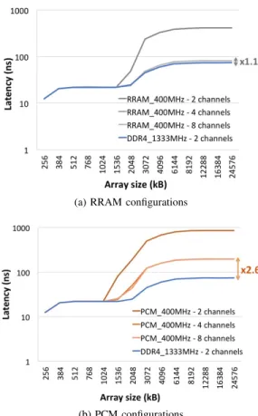
B. Number of Channels
Now, we evaluate the impact of the channel count in the main memory architecture. In the previous memory design sce-narios, we only considered two channel memory technologies. More generally, memory architectures with multiple channels aim at increasing the data transfer rate between the memory and its associated controller by multiplying the number of communication channels between them. Since memory chan-nels are expensive resources, the number of memory chanchan-nels is a design-decision that is heavily influenced by the targeted market. The subsequent evaluation is conducted within the framework of the MontBlanc3 European project which aims at developing an ARMv8-based pre-exascale supercomputer. Because of that the actual cost is less of an issue compared to a mobile market: the current prototype, named Dibona and based on Marvell ThunderX2 CPUs, has been devised by the Atos Company and includes 8 DDR4 channels per socket.
Figure 12 summarizes the memory latency evaluation for different multi-channel memory architectures. The number of channels is varied from 2 to 8 for NVMs, while the reference DDR4 memory architecture is kept unchanged with 2 chan-nels. Figure 12a shows the potential improvement achieved for the RRAM technology with architectures including either 4 or 8 channels. The latency gap of RRAM technology is decreased up to x1.1 compared to the baseline DDR4 technology, i.e., almost equivalent latencies. When considering the PCM technology, the latency gap w.r.t. DDR4 is reduced up to x2.6, which is also quite relevant. To minimize the cost of the memory system, selecting 4 channels instead of 8 represents a satisfactory compromise for NVM integration.
Multi-channel memory architectures, therefore, provide an interesting opportunity for mitigating the latency overhead of NVMs. While the latency improvement enabled here is higher than that obtained through memory interface frequency upscaling, both opportunities could be combined for further gains.
C. NVM-specific Memory Controllers?
Another design question regarding the successful integration of NVMs in computer systems concerns adequate control mechanisms at the hardware level. Indeed, memory controllers play a central role in data allocation and movement within the main memory for meeting the low latency, high throughput, and optimized energy requirements.
In the present study, all experiments have been achieved by considering the controller configuration given by default in NVMaim models: FRFCFS controller for both DDR4 and
(a) RRAM configurations
(b) PCM configurations
Fig. 12: Comparison of NVM memory system latencies with 2, 4 and 8 channels versus the reference DDR4 configuration (zoom from L2 cache to main memory)
RRAM, and FRFCFS-WQF controller for PCM. This leaves room for further design optimizations since the memory ac-cesses have variable costs depending on the selected controller. Typically, the average main memory latency of PCM can be reduced by 16% by selecting the FRFCFS controller instead of FRFCFS-WQF. Furthermore, the row buffer design inside the controller could take into account the different latencies of hits and misses depending on the memory technology: DRAM and PCM are known to have similar row buffer hit latency, while the row buffer miss latency is larger for PCM due to their related higher array access latency [11].
The aforementioned controller design should exploit the het-erogeneous/homogeneous nature of the main memory. Some existing work already addressed the case of hybrid DRAM-NVM main memory design, where row buffer locality-aware data placement policies are proposed [61]. For instance, the au-thors observed that streaming data accesses are PCM-friendly, while other data accesses (with reuse) are rather DRAM-friendly for data placement. In the case of main memory integrating only NVM, as evaluated in the present work, the design of the memory controller is an open question that remains to be addressed. We believe that revisiting the design principle of such a mechanism can improve the benefits of NVM integration by taking their specificity into account.
VI. GAINED INSIGHTS FORSOCINTEGRATION
From all the previous experimental results, we draw more concretely the envisioned most favorable NVM integration in the memory hierarchy beyond cache levels. We briefly address the programmability issue of compute nodes in presence of NVMs in main memory.
A. General observations
Our experiments show that NVM can relevantly improve the main memory energy consumption, at the expense of limited penalty on performance. The announced cost-effectiveness6of
these emerging memory technologies compared to concurrent technologies, such as DRAM and NAND Flash, makes this perspective credible. Given a relative cost per bit of 1 for DRAM, it is around 0.25 for PCM and RRAM [37].
The perspective of their integration in future SoCs is par-ticularly promising with the RRAM technology, while PCM may incur non-negligible performance degradation. The PCM technology rather appears as an in-between good candidate w.r.t. faster main memories and slower storage-class memories (this observation additionally holds for the recent 3D XPoint technology from Intel and Micron [26]. It is worth-mentioning that NVMain only enables to model and evaluate main mem-ory level technology integration. Dealing with storage level integration would require new simulation tools. Figure 13 summarizes this idea.
Fig. 13: Memory technologies within memory hierarchy. Note that our study does not consider alternative NVM integration approaches, such as hybrid memory design as addressed widely in existing literature [11]. These approaches are a complementary solution that may have an impact on the way NVM integration is seen through the memory hierarchy depicted in Figure 13.
Actually, the joint emergence of HBM and NVM technolo-gies will likely lead to revisit the junction between memory hierarchy and storage as we know it in today’s systems. Indeed, why would designers keep on considering the DRAM technology for main memory, while NVM could provide all the necessary memory capacity? On the other hand, why would industry keep on deploying chips with hard drive supports while NVM controllers could help to fill this demand? Remov-ing all unnecessary design features has been always the point for the design of optimized ARM-based HPC SoCs to save power and increase the system energy-efficiency. Therefore, for high-end server capability such as in HPC domain, a new
6
memory design trade-off is definitely to be found between DRAM, NVMs and SATA connection in the near future. B. Impact on programming models
Beyond the above architectural design considerations, the integration of NVMs in multicore SoCs calls for reconsidering the entire system design stack. This concerns in particular the impact on programming models and system software. In order to anticipate this issue, we evaluate two parallel programming models through different versions of the same application while having NVMs in main memory. These programming models are supposed to involve different memory activities according to their associated runtime management systems.
We consider the OpenMP version 2.3 and OmpSs program-ming models. OpenMP7 is a popular shared-memory parallel
programming interface. The OpenMP version 2.3 (in which our benchmarks and mini-applications are implemented) fea-tures a thread-based fork-join task allocation model as illus-trated in Figure 14a. It consists of a set of compiler directives, library routines and environment variables for the development of parallel applications. OmpSs [62] is a task-based program-ming model (see Figure 14b) that improves OpenMP with support for irregular and asynchronous parallelism, and for heterogeneous architectures. It incorporates dataflow concepts enabling its compiler/runtime to automatically move data whenever necessary and to apply various useful optimizations.
(a) OpenMP (b) OmpSs
Fig. 14: OpenMP fork-join region vs OmpSs task graph The Nanos++ runtime used with OmpSs enables an asymmetry-conscious task scheduling [63]. It incorporates Criticality-Aware Task Scheduler (CATS) scheduling policy CATS, which exploits the criticality of generated tasks to schedule them during execution. The most critical tasks, i.e., those appearing on the critical execution path, are executed by the high-frequency cores. Typically, such tasks are represented in red color in Figure 14b. Less critical tasks are executed on low-power cores. These tasks are denoted by green color in Figure 14b.
To compare both programming models, we consider two corresponding versions of the HPCCG mini-application. We observe that the OmpSs version of HPCCG provides better performance than the OpenMP version. This is mainly due to the CATS scheduler of the former. On the other hand, the read/write bandwidth obtained with OmpSs version, shown
7https://www.openmp.org
in Figure 15, is significantly higher than that of OpenMP version (see Figure 9). For instance, the read bandwidth is improved by about 4x, 3x and 1.8x for DDR4, RRAM, and PCM respectively. However, the write bandwidth is improved merely marginally.
Fig. 15: Main memory bandwidth for OmpSs version of HPCCG with DDR4.
The impact of this improvement is illustrated in Figure 16. The execution time and main memory energy consumption are compared separately for each memory technology, according to the two programming models for HPCCG. The OmpSs run-time enables to reduce by more than 50% the execution run-time of the OpenMP version for all three memory technologies. This is in-line with our previous observations when comparing both programming models [64]. It additionally allows a reduction of energy consumption, by 60% for DDR4 and by 20% for PCM. However, it marginally increases the energy consumption for RRAM (around 2%). This is due to the notable increase in write bandwidth enabled by OmpSs scheduler, specifically for RRAM. Writes on NVMs are very expensive operations both in latency and energy consumption.
VII. CONCLUDING REMARKS
In this paper, we evaluated two relevant emerging NVM technologies at the main memory level, to analyze their impact on both system performance and main memory energy. Key motivation is to quantify as much as possible the impact of NVMs in explored design scenarios. Starting from the PCM and RRAM model templates provided by the NVMain simula-tion framework, we enhanced them through some extrapolasimula-tion relying on existing literature. The NVM integration has been evaluated with the gem5 cycle-approximate simulator while considering a heterogeneous ARMv8 multicore system model (such systems are envisioned as good candidates for compute node design in HPC domain [2]). A subset of representative Parsec benchmarks and two typical mini-applications from HPC domain have been used as evaluation workloads.
Our experiments showed RRAM represents a very good candidate for energy issue mitigation at the main memory level, while PCM would be a better candidate for storage level. RRAM is competitive enough compared to DDR4 from the viewpoint of system-level performance. Most importantly,
(a) Normalized execution time
(b) Normalized energy consumption
Fig. 16: Separate comparison per memory technology for HPCCG mini-application: OpenMP vs OmpSs
it enables a reduction of main memory energy consumption by up to 50%. While PCM does not offer such benefits at the main memory level, it could be a more suitable candidate for storage level. Currently, at storage level solutions for the server market are mostly implementing SSD drives: through CPU SATA features or through PCIe devices for NVMe disks. PCM appears a viable alternative for high-performance storage as well as for high-performance computing. Nonetheless, to sustain this gain expected from emerging NVMs, complemen-tary mechanisms (e.g., targeting wear-leveling) or technology improvements regarding write endurance will be helpful. Some candidate solutions already exist [23].
It is worth-mentioning that the experiments conducted in this study rely on NVM models published in 2012 by Samsung and Panasonic. This decision was motivated by the high-level of confidence on these published results. These rather old models can be seen as conservative approximations of these technologies and their potential: the state-of-the-art on NVM technologies has notably improved over the last years and the gains observed in this study might get better as NVM technologies progress.
ACKNOWLEDGMENT
This work was supported in part by the Mont-Blanc3 H2020 project under the grant number 671697, and the CONTIN-UUM French ANR project under the grant number ANR-15-CE25-0007-01.
REFERENCES
[1] K. Bergman, S. Borkar, D. Campbell, W. Carlson, W. Dally, M. Den-neau, P. Franzon, W. Harrod, J. Hiller, S. Karp, S. Keckler, D. Klein, R. Lucas, M. Richards, A. Scarpelli, S. Scott, A. Snavely, T. Sterling,
R. S. Williams, K. Yelick, K. Bergman, S. Borkar, D. Campbell, W. Carl-son, W. Dally, M. Denneau, P. Franzon, W. Harrod, J. Hiller, S. Keckler, D. Klein, P. Kogge, R. S. Williams, and K. Yelick, “ExaScale Computing Study: Technology Challenges in Achieving Exascale Systems Peter Kogge, Editor & Study Lead,” 2008.
[2] J. Wanza Weloli, S. Bilavarn, M. De Vries, S. Derradji, and C. Belleudy, “Efficiency modeling and exploration of 64-bit arm compute nodes for exascale,” Microprocess. Microsyst., vol. 53, no. C, pp. 68–80, Aug. 2017. [Online]. Available: https://doi.org/10.1016/j.micpro.2017.06.019 [3] J. Boukhobza, S. Rubini, R. Chen, and Z. Shao, “Emerging nvm:
A survey on architectural integration and research challenges,” ACM Trans. Des. Autom. Electron. Syst., vol. 23, no. 2, pp. 14:1–14:32, Nov. 2017. [Online]. Available: http://doi.acm.org/10.1145/3131848 [4] J. Russell, “Cavium Announces GA for ThunderX2;
Touts OEM Support,” https://www.hpcwire.com/2018/05/07/ cavium-announces-ga-for-thunderx2-touts-oem-support/, [Accessed: May 7, 2018].
[5] S. M. Tam, H. Muljono, M. Huang, S. Iyer, K. Royneogi, N. Satti, R. Qureshi, W. Chen, T. Wang, H. Hsieh et al., “Skylake-sp: A 14nm 28-core xeon processor,” in Solid-State Circuits Conference-(ISSCC),R
2018 IEEE International. IEEE, 2018, pp. 34–36.
[6] J. Dongarra, M. A. Heroux, and P. Luszczek, “High-performance conjugate-gradient benchmark,” Int. J. High Perform. Comput. Appl., vol. 30, no. 1, pp. 3–10, Feb. 2016. [Online]. Available: https://doi.org/10.1177/1094342015593158
[7] S. McIntosh-Smith, J. Price, T. Deakin, and A. Poenaru, “Comparative benchmarking of the first generation of hpc-optimised arm processors on isambard,” in Cray User Group, 5 2018.
[8] T. Yoshida, M. Hondou, T. Tabata, R. Kan, N. Kiyota, H. Kojima, K. Hosoe, and H. Okano, “Sparc64 xifx: Fujitsu’s next-generation processor for high-performance computing,” Micro, IEEE, vol. 35, pp. 6–14, 03 2015.
[9] M. Feldman, “Fujitsu Reveals Details of Processor That Will Power Post-K Supercomputer,” https://www.top500.org/news/ fujitsu-reveals-details-of-processor-that-will-power-post-k-supercomputer/, [Accessed: August 22, 2018].
[10] HUAWEI, “Huawei Unveils Industry’s Highest-Performance ARM-based CPU,” https://www.huawei.com/en/press-events/news/2019/1/ huawei-unveils-highest-performance-arm-based-cpu, [Accessed: Jan 07, 2019].
[11] O. Mutlu, “Opportunities and challenges of emerging memory technolo-gies,” 2017, invited Talk during ARM Research Summit.
[12] K. Lim, J. Chang, T. Mudge, P. Ranganathan, S. K. Reinhardt, and T. F. Wenisch, “Disaggregated memory for expansion and sharing in blade servers,” SIGARCH Comput. Archit. News, vol. 37, no. 3, pp. 267–278, Jun. 2009. [Online]. Available: http://doi.acm.org/10.1145/ 1555815.1555789
[13] O. Mutlu and L. Subramanian, “Research problems and opportunities in memory systems,” Supercomput. Front. Innov.: Int. J., vol. 1, no. 3, pp. 19–55, Oct. 2014. [Online]. Available: http://dx.doi.org/10.14529/ jsfi140302
[14] C. Lefurgy, K. Rajamani, F. Rawson, W. Felter, M. Kistler, and T. W. Keller, “Energy management for commercial servers,” Computer, vol. 36, no. 12, pp. 39–48, Dec. 2003. [Online]. Available: https://doi.org/10.1109/MC.2003.1250880
[15] I. Bhati, M.-T. Chang, Z. Chishti, S.-L. Lu, and B. Jacob, “Dram refresh mechanisms, penalties, and trade-offs,” IEEE Trans. Comput., vol. 65, no. 1, pp. 108–121, Jan. 2016. [Online]. Available: http://dx.doi.org/10.1109/TC.2015.2417540
[16] S. Bhatti, R. Sbiaa, A. Hirohata, H. Ohno, S. Fukami, and S. Piramanayagam, “Spintronics based random access memory: a review,” Materials Today, vol. 20, no. 9, pp. 530 – 548, 2017. [Online]. Available: http://www.sciencedirect.com/science/article/ pii/S1369702117304285
[17] S. Senni, L. Torres, G. Sassatelli, A. Gamati´e, and B. Mussard, “Ex-ploring mram technologies for energy efficient systems-on-chip,” IEEE Journal on Emerging and Selected Topics in Circuits and Systems, vol. 6, no. 3, pp. 279–292, Sep. 2016.
[18] S. Senni, T. Delobelle, O. Coi, P. Peneau, L. Torres, A. Gamati´e, P. Benoit, and G. Sassatelli, “Embedded systems to high performance computing using stt-mram,” in Design, Automation Test in Europe Conference Exhibition (DATE), 2017, March 2017, pp. 536–541. [19] R. Bouziane, E. Rohou, and A. Gamati´e, “Compile-time silent-store
elimination for energy efficiency: an analytic evaluation for non-volatile cache memory,” in Proceedings of the RAPIDO 2018 Workshop on Rapid Simulation and Performance Evaluation: Methods and Tools,