HAL Id: hal-01876410
https://hal.sorbonne-universite.fr/hal-01876410
Submitted on 21 Sep 2018
HAL is a multi-disciplinary open access archive for the deposit and dissemination of sci-entific research documents, whether they are pub-lished or not. The documents may come from teaching and research institutions in France or abroad, or from public or private research centers.
L’archive ouverte pluridisciplinaire HAL, est destinée au dépôt et à la diffusion de documents scientifiques de niveau recherche, publiés ou non, émanant des établissements d’enseignement et de recherche français ou étrangers, des laboratoires publics ou privés.
Evolution of interfacial structure of Co-based periodic
multilayers upon annealing
Yanyan Yuan, Karine Le Guen, Christian Mény, Corinne Bouillet, Jingtao
Zhu, Zhanshan Wang, Philippe Jonnard
To cite this version:
Yanyan Yuan, Karine Le Guen, Christian Mény, Corinne Bouillet, Jingtao Zhu, et al.. Evolution of in-terfacial structure of Co-based periodic multilayers upon annealing. Surface and Coatings Technology, Elsevier, 2018, 352, pp.508 - 512. �10.1016/j.surfcoat.2018.08.054�. �hal-01876410�
1
Evolution of interfacial structure of Co-based periodic multilayers upon annealing
Yanyan Yuan1*, Karine Le Guen2, Christian Mény3, Corinne Bouillet3, Jingtao Zhu4, Zhanshan
Wang4, Philippe Jonnard2
1National Demonstration Center for Experimental Materials Science and Engineering Education (Jiangsu University of Science and Technology), Zhenjiang 212003, People’s Republic of China
2 Sorbonne Université, Faculté des Sciences et Ingéniérie, UMR CNRS, Laboratoire de Chimie Physique-Matière et Rayonnement, 4 place Jussieu, F-75252 Paris cedex 05, France
3 Institut de Physique et Chimie des Matériaux de Strasbourg, UMR 7504 CNRS-Université De Strasbourg 23 rue du Loess, 67034 Strasbourg, France
4 Institute of Precision Optical Engineering, Department of Physics, Tongji University, Shanghai 200092, China
Abstract
The evolution upon annealing from room temperature to 600°C of the microstructure of Co/Mo2C/Y and Co/Y/Mo2C multilayer stacks has been studied by transmission electron
microscopy combining HAADF-STEM, EDX and HRTEM. Both kinds of samples show significant amount of intermixing even in the as-deposited state. The mixing further increases upon annealing. Most of the mixing occurs between the Co and the Mo elements, the Y layers staying comparatively preserved. After annealing at 600°C a surprising sharpening of the interfaces is observed. It is ascribed to the formation of Co-Mo compounds. Combining these new analyses with the results we have already published, we can explain in a consistent way the evolution of the x-ray reflectivity measurements of the samples upon annealing. Understanding the evolution the optical properties of such stacks designed to work in the soft x-ray range is essential for improving the optical performance of multilayer structures.
Keywords: Co-based multilayer; interface structure; annealing; intermixing; STEM; HAADF
2 1. Introduction
Multilayer mirrors are important optical elements in the soft x-ray and extreme ultraviolet (EUV) ranges [1-4]. The peak reflectivity of a multilayer mirror is critically dependent on the quality of each layer and interface in the stack [5-7]. Formation of continuous and smooth layers is important for achieving good optical performance of multilayer optics. Therefore, the accurate observation of microstructural features and interfacial structures, like intermixing and interface reaction, is necessary to improve the optical properties of the mirrors. In addition, studying the stability of the stacks under annealing is also important in order to simulate and understand the aging of such artificial structures. In this framework, the estimate of the width of interfaces and interlayers is generally provided from the fit of hard x-ray reflectivity data [8,9]. However as exemplified in this work x-ray reflectivity data cannot solely provide a complete description of such system. Thus, observation of direct imaging in electron microscopy is an essential counterpart to the fitting of the XRR data.
In our previous paper, using non-destructive methods [10], it has been reported that the Co/Mo2C/Y systems showed a compression of their period owing to the formation of
interfacial compounds. To understand exactly the origin of this period compression, the interface microstructure needs to be further clarified. In this paper, we used a scanning transmission electron microscope (STEM) equipped with high-angle annular dark field (HAADF) detector to analyze the microstructure of the multilayers. Unlike bright field (BF) imaging, HAADF imaging reduces the diffraction and phase contrast and the collected signal is dependent on the atomic number Z [11, 12], the shape of the atom and the total number of atoms encountered by the electron probe. Therefore, HAADF STEM image intensity is highly sensitivity to the atomic number (Zn with 1.5 < ! < 2.0) [13, 14]. It has been used to investigate materials on the atomic scale with chemical sensitivity. For examples, Robb et al. demonstrated that the interfacial sharpness of the AlAs-on-GaAs interfaces can be effectively,
3
and quantitative analysis of the Ga(AsBi) and GaSb/GaAsSb systems was achieved via [15, 16]. It was also demonstrated that HAADF-STEM technique is highly effective compared to bright-field STEM for studying interfaces of Mo/Si multilayer structures [17]. Furthermore, the study of an aperiodic W/B4C multilayer system demonstrated the reliability of the
HAADF-STEM technique regarding the quantification of layer thicknesses [18].
Scanning transmission electron microscopy energy-dispersive X-ray (STEM-EDX) spectroscopy technique is also used in this study to determine element distribution for acquiring the interfacial information. STEM-EDX owns relatively high spatial resolution and is a very reliable approach to explore elemental composition. By acquiring an EDX spectrum in atomic resolution, all major elements can be easily recognized at any measured point [19]. For example, Servanton et al. reported that STEM-EDX is effective to detect the low arsenic
dopant concentration in silicon devices at the nanometer scale [20] and Chen et al. pointed that precise elemental composition can be acquired by the improvement of detector collection angle and stability [21].
The aim of the present work is to investigate in details the structure of Co/Mo2C/Y and
Co/Y/Mo2C periodic multilayers. Using TEM and HAADF-STEM as well as STEM-EDX,
we study the layer chemical change upon annealing in these two systems. Interface widths are evaluated from intensity profile on bright field images. We compare the interface structures of each system annealed at 300 and 600°C. The accurate analysis of the layers microstructure should help us understanding the reduction of the reflectivity performances of multilayer mirrors upon annealing and also improving further multilayer mirrors design.
2. Experimental 2.1 Sample preparation
Co/Mo2C/Y systems were prepared by direct-current magnetron sputtering. The
substrates were sliced and polished Si (100) wafers. We have changed the order of deposition of two materials in one period in order to distinguish the effect of the two interfaces on the
4
reflectivity [10, 22]: in the following, Co/Mo2C/Y and Co/Y/Mo2C samples are studied. The
first layer close to the substrate is Co and Mo2C for the Co/Mo2C/Y and Co/Y/Mo2C systems,
respectively. The last layer is the Y layer in the both multilayers. The designed period is 7.7 nm and the nominal thickness of Co, Mo2C and Y layers are 1.0 nm, 2.7 nm and 4.0 nm,
respectively. A 3.5 nm-thick B4C capping layer has been deposited to prevent oxidation. The
number of periods is 30. The base pressure was 10-5 Pa before deposition. The working gas
was argon (99.999% purity) at a constant working pressure equal to 0.1 Pa. There were six 10×10 mm2 substrate sections cleaved from a single wafer for each system. Then six multilayers were deposited separately in the same conditions. For each multilayer, five samples were annealed at different temperatures ranging from 200°C to 600°C with an interval of 100°C for one hour in a furnace with a base pressure of 3.0×10⁻⁴ Pa. For this paper
we show the results obtained for five samples: the Co/Mo2C/Y multilayers, as-deposited and
annealed at 300 and 600°C, and the Co/Y/Mo2C multilayers, annealed at 300 and 600°C.
TEM cross sections were prepared by mechanical grinding and ion milling. First, two lamellae of 3×5 mm were glued face to face with a M-Bond 610 epoxy in order to obtain a sandwich, which was sliced into 750 µm thick pieces using a precision diamond wire saw instrument. TEM thin foil were prepared first by a mechanical polishing until a sample thickness of 30 µm is obtained and followed by an ion milling process until a small hole was drilled through the sample.
The high-resolution TEM images and selected-area electron diffraction (SAED) were performed using a JEOL 2100F microscope operating at 200 kV and equipped with a spherical aberration corrector on the condenser lenses. The point to point resolution was 0.20 nm in HRTEM and 0.12 nm in the HAADF-STEM modes respectively. The convergence angle was 25 mrad and the collection angles spread from 80 to 214 mrad. EDX line scan on the dark field image were performed to determine the distribution of the elements in each layer. The EDX detector is a JEOL Si(Li) detector. A point on the scan line lasted two
5
minutes. The beam current was around 150 pA and the beam size 0.15 nm. A drift correction by cross correlation was performed every 30 s. The interface widths were evaluated by measuring on the line profiles the positions reaching 15 and 85% of the maximum intensity. A similar evaluation method is mentioned by Kessels et al [23].
3. Results and discussion
3.1 Scanning transmission electron microscopy (STEM)
Fig. 1(a) and (b) present the HAADF images of the Co/Mo2C/Y as-deposited and
Co/Y/Mo2C 600°C annealed samples, respectively. They show that even though our
multilayers are constituted by 3 different materials only two clearly different contrasts can be observed. In an HAADF image, the contrast depends on the average atomic number of the elements: the bright regions correspond to the high atomic number (high-Z) element. In our case, we need to calculate the average atomic number of Co, Mo2C and Y materials per cubic
Ångström. According to Hartel et al [24], considering the Rutherford–like diffusion, all atoms should be added in one given irradiated volume. The contrast in the HAADF STEM image is approximately proportional to Z power 1.7 [25]. So for Co, there are two atoms in the volume of 22 cubic Ångströms and the average atomic number is equal to [271.7×2]/22=24.5. For
Mo2C, the cell contains eight atoms of Mo and four atoms of C in a volume of 148 cubic
Ångströms and the average atomic number is equal to [(421.7×8)+(61.7×4)]/148=30. For Y, there are four atoms in a volume of 123 cubic Ångströms and the average atomic number is equal to [391.7×4]/123=16. Thus if no diffusion takes place between layers, the brightest regions should indicate the Mo2C layers in the stack. However the average atomic number of
Co is only slightly smaller than the one of Mo2C and will therefore only be slightly less bright
than Mo2C. From the order of deposition, the first three layers close to the substrate are Co,
Mo2C, Y and Mo2C, Co, Y layers for Co/Mo2C/Y and Co/Y/Mo2C systems, respectively.
Therefore, in both multilayer types, the bright regions correspond to both Co and Mo2C layers
6
atomic number between Co and Mo2C it is difficult to conclude if interdiffusion takes place
between the Co and Mo2C layers or not. However, in a previous paper [10], we have
demonstrated that the fits of the EUV reflectivity data of both systems were improved when considering interdiffusion and compound formation between the layers.
Because the small HAADF contrast between Co and Mo2C does not allow
characterizing the interfaces between Co and Mo2C, we have performed EDX measurements
in order to get a better insight into the interface quality of the stacks. Fig. 2(a)-(e) show the EDX line profiles performed in the HAADF-STEM mode for the five samples. As already suggested, it is confirmed that the Y layers do correspond to the dark regions while both the Mo2C and Co layers correspond to the bright regions. In the case of the as-deposited
Co/Mo2C/Y sample, Fig. 2(a), the Mo concentration profile extends all over the Co
concentration range. A shoulder in the Mo profile can even be observed in the Co concentration range. From the point of view of Y, the maximum of its concentration profile corresponds to the minimum of concentration of Mo and Co. Similar observation can be made for Co/Mo2C/Y annealed at 300°C (Fig. 2(b)). The Mo concentration profile shoulder in the
Co range appears even more clearly than at room temperature. This shows that the Co layers do fully mix with Mo or Mo2C and form an interphase between the Y and Mo2C layers. When
annealing temperature is increased up to 600°C the shoulder in the Mo concentration profile is less clear again but at the same time Co concentration is observed in the Y range meaning that an even more general mixing occurs at 600°C temperature.
For the Co/Y/Mo2C_300°C and 600°C samples, Fig. 2(d) and (e), as for the previous
samples the Mo concentration profile does extend over the Co concentration range. In addition, the Mo concentration profile also extends into the Y range. The Co seems to extend much less in the Y range.
7
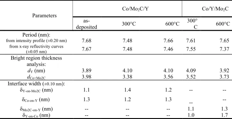
For the sake of comparison with our previous hard x-ray reflectivity data we performed line intensity profiles that give similar information. Fig. 3 presents an example of line profile along a few periods, extracted from the bright field image of a typical sample. These intensity line profiles are related to the density of materials and the cross-sectional lamella sample thickness. The position of the pure Y layers in the stack corresponds to the bright layers as the contrast in bright field STEM image is opposite to that in dark field ones. The period thickness is determined by calculating the distance between two peaks. In order to minimize the aberration of period value, we take the average value obtained over almost all the thickness of the stack. The results obtained for the five samples, are listed in Table 1 and compare well with the values deduced from the hard x-ray reflectivity data [10].
In order to obtain the detailed information about the layer period and the interface width between layers, the intensity line profile of one period is magnified as shown in Fig. 3(b). The thickness of bright regions can be determined by calculating the full width at half maximum (FWHM) in the intensity line profile. These values are also listed in Table 1. They are close to the designed thickness of Y layer. The Mo2C and Co layers in all samples
are mixed and thus cannot be discerned. The thicknesses of these mixed layers are obtained by subtracting the Y layer thickness from the period, see Table 1. They slightly differ from the fitted values derived from the XRR data (not shown).
The line profiles can also be used to evaluate the interface width. For the as-deposited Co/Mo2C/Y multilayer, the width of the Y-on-Mo2C interface is determined to be 1.1 nm and
slightly smaller than that of Co-on-Y interfaces (1.3 nm). Considering the uncertainty (± 0.10 nm), the width of these two interfaces shows no significant variation upon annealing. For the Co/Y/Mo2C multilayers, the interface widths of the Mo2C-on-Y and Co-on-Y interfaces are
determined to be 1.1 and 1.0 nm respectively at 300°C, rather similar given the uncertainty. At 600°C, both interface widths increase and the value of Y-on-Co interface (1.7 nm) is larger than that of the Mo2C-on-Y interface (1.3 nm), evidencing asymmetrical interfaces.
8 3.3 High-resolution TEM images
In the previous paragraphs it is shown that the multilayers are strongly mixed, especially at the Co/Mo2C interfaces. In this part using high-resolution TEM images, further
investigation of the crystallographic nature of the layers and intermixed regions are presented. Fig. 4(a)-(e) show the high-resolution TEM images of both Co/Mo2C/Y and Co/Y/Mo2C
systems. In all the samples, lattice fringes are revealed with different orientations. The bright regions correspond to polycrystalline Y layers. From the lattice fringes, it is possible to determine an interatomic distance of the order of 0.3 nm. It is also determined by the selected-area electron diffraction images, inserts of Fig. 4(a), (d) and (e). This distance can only be attributed to pure Y lattice. However yttrium carbides also show similar interatomic distances, therefore the presence of carbon into the Y layer cannot be ruled out. No lattice fringes are observed in the dark regions that correspond to the Mo2C and Co layers. It does not mean that
these regions are amorphous but only that the TEM beam is not aligned with any lattice orientation. In our previous work [10] X-ray reflectivity data simulations suggested the presence of MoC and Co2Y phases. However lattice fringes corresponding to these phases are
not observed and the presence of these phases cannot be confirmed. Fig. 4(b) and (d) show that after annealing at 300°C the contrast between the dark and bright regions becomes weaker. This is consistent with the layer intermixing shown in the previous paragraphs. Indeed as intermixing becomes larger the difference in average atomic number becomes smaller what results in a decrease in contrast. Surprisingly Fig. 4(c) and (e) show that after annealing at 600°C the contrast between the bright and dark regions increases again. This has already been mentioned in the HAADF images analysis. Although no direct evidence can be given, this suggests that well defined compounds, like the MoC and Co2Y phases introduced
in the X-ray reflectivity simulations [10], are formed.
Considering the information obtained by this study and by our previous results [10], we can attempt to explain the behavior of the sample reflectivity [10]. In the as-deposited
9
samples interfacial mixing between the different layers already exists (for example by the nuclear magnetic resonance spectroscopy) the mixing is smaller in the Co/Mo2C/Y
as-deposited sample. It results in a significantly larger reflectivity for the Co/Mo2C/Y samples.
Upon annealing diffusion occurs in both samples reducing the reflectivity of both samples. The EDX line profiles suggest that the mixing takes place over the whole layers in the Co/Y/Mo2C sample while it is limited to an interphase in the Co/Mo2C/Y sample. It results in
a stronger decrease of the Co/Y/Mo2C reflectivity. Finally at 600°C a dramatic increase of
Co/Y/Mo2C reflectivity is observed that becomes almost as large as the one obtained for the
as deposited Co/Mo2C/Y layer. This is attributed to the formation of new phases during this
high temperature annealing. However the MoC and Co2Y phases suggested by the reflectivity
simulations are not consistent with our present results. Indeed both EDX analysis and HRTEM measurements suggest that the Y layers stay rather free of mixing. On the other hand EDX results show that Co is fully mixed with Mo. So the phases formed at high temperature are more likely to be Co-Mo phases resulting in a sharpening of the interfaces. This sharpening is also observed by HRTEM in the Co/Mo2C/Y sample. However the EDX
analysis suggests that the Co-Mo phase formation is limited to the interfacial regions (shoulder in the profile) while in the Co/Mo2C/Y samples it probably takes place all over the
Co/Mo part of the stack (same maximum position for Co and Mo in the EDX profile). The behavior of the carbon atoms with annealing is more complicated to ascertain. Most likely while Co and Mo atoms mix together [26], carbon atoms enter the Y layers without significantly modifying the lattice fringes observed by HRTEM.
4. Conclusion
The evolution upon annealing from room temperature to 600°C of the microstructure of Co/Mo2C/Y and Co/Y/Mo2C multilayer stacks has been studied by transmission electron
microscopy combining HAADF-STEM, EDX and HRTEM. Both kinds of samples show significant amount of intermixing even in the as-deposited state. The mixing increases upon
10
annealing. Most of the mixing occurs between the Co and the Mo elements, the Y layers staying comparatively preserved. After annealing at 600°C a surprising sharpening of the interfaces is observed. It is attributed to the formation of Co-Mo compounds. Combining these analyses with the results published in [10] we can explain in a consistent way the evolution of the X-ray reflectivity measurements of the samples upon annealing. The observation of transmission electron microscopy provides a meaningful suggestion to improve the reflectivity of samples including several components.
Acknowledgments
This work was supported by the international ANR-NSFC COBMUL project (ANR #10-INTB-902-01) and NSFC project #11061130549 and NSFC project #51702133.
References
[1] A. V. Vinogradov and S. I. Sagitov,New types of mirrors for the soft x-ray range, Sov. J.
Quantum Electron, 13, 11(1983)1439-1446.
[2] S.S. Andreev, H.-Ch. Mertins, Yu.Ya. Platonov, N.N. Salashchenko, F. Schaefers, E.A. Shamov, L.A. Shmaenok , Multilayer dispersion optics for X-ray radiation, Nuclear
Instruments and Methods in Physics Research A, 448 (2000) 133-141.
[3] D. L. Windt, S. Donguy, J. Seely, B. Kjornrattanawanich, E. M. Gullikson, C. C. Walton, L. Golub and E. DeLuca, EUV Multilayers for Solar Physics, Proceedings of SPIE, Optics for
EUV, X-Ray, and Gamma-Ray Astronomy, 5168(2004)1-11.
[4] M.G. Pelizzo, A.J.Corso, P.Zuppella, P.Nicolosi, Multilayer coatings and their use in spectroscopic applications, Nuclear Instruments and Methods in Physics Research, A720(2013)49–52.
[5] Karen Holloway, Khiem Ba Do, and Robert Sinclair,Interfacial reactions on annealing molybdenum silicon multilayers,J. Appl. Phys, 65, 2 (1989)474-480.
[6] D. G. Stearns, M. B. Stearns, Y. Cheng, J. H. Stith, and N. M. Ceglio, Thermally induced structural modification of Mo/Si multilayers, J. AppL Phys, 67, 5 (1990)2415-2427.
11
[7]V.I.T.A. de Rooij-Lohmann, A.E. Yakshin, E. Zoethout, J. Verhoeven, F. Bijkerk, Reduction of interlayer thickness by low-temperature deposition of Mo/Si multilayer mirrors for X-ray reflection, Appl. Surf. Sci., 257 (2011) 6251–6255.
[8] Y. Y. Yuan, Karine Le Guen, Jean-Michel André, Zhanshan Wang, Haochuan Li, Jingtao Zhu, Christian Mény, Angelo Giglia, Stefano Nannarone, Philippe Jonnard, Co/Mo2C
multilayer as X-ray mirror: Optical and thermal performances, Phys. Status Solidi B, 251, 4 (2014) 803–808.
[9] Y. Y. Yuan, Karine Le Guen, Jean-Michel André, Christian Mény, Corinne Ulhaq, Anouk Galtayries, JingTao Zhu, Zhanshan Wang, Philippe Jonnard, Interface observation of heat-treated Co/Mo2C multilayers, Appl. Surf. Sci., 331 (2015) 8–16.
[10] Y. Y. Yuan, Karine Le Guen, Jean-Michel André, Zhanshan Wang, Jingtao Zhu, Christian Mény, Philippe Jonnard, Optical and structural characterization of the Co/Mo2C/Y
system, Appl. Surf. Sci., 315 (2014) 499–505.
[11] J. Liu and J.M. Cowley, High-resolution scanning transmission electron microscopy,
Ultramicroscopy, 52 (1993) 335-346.
[12] Ian MacLaren and Quentin M. Ramasse, Aberration-corrected scanning transmission electron microscopy for atomic-resolution studies of functional oxides
, International Materials Reviews,59, 3(2014) 115-131.
[ 13 ] S.J. Pennycook, D.E. Jesson, High-resolution Z -contrast imaging of crystals,
Ultramicroscopy, 37, 1(1991) 14–38.
[14] S. J. Pennycook, D. E. Jesson, High-resolution incoherent imaging of crystals, Phys. Rev.
Lett., 64, 8 (1990) 938–941.
[15] N. Knaub , A. Beyer , T. Wegele , P. Ludewig , K. Volz , Quantification of Bi distribu- tion in MOVPE-grown Ga(AsBi) via HAADF STEM, J. Cryst. Growth 433 (2016) 89–96. [16] H. Kauko, T. Griebb, R. Bjørge, M. Schowalter, A.M. Munshi, H. Weman, A. Rosenauer, A.T.J. van Helvoort, Compositional characterization of GaAs/GaAsSb nanowires by quantitative HAADF-STEM, Micron, 44 (2013) 254–260.
[17] J. Liu, Y. Cheng, J. M. Cowley and M. B. Stearns, High-angle annular dark-field microscopy of Mo/Si multilayer structures, Ultramicroscopy, 40, 3 (1992) 352–364.
[18] D. Häussler, Ch. Morawei, U. Roß, B. Ögüt, E. Spiecker, W. Jäger, F. Hertlein, U. Heidorn, J. Wiesmann, Aperiodic W/B4C multilayer systems for X-ray optics: Quantitative
determination of layer thickness by HAADF-STEM and X-ray reflectivity, Surf. Coat.
Technol., 204, 12–13 (2010) 1929–1932.
[19] Stephen J. Pennycook, Peter D. Nellist(Eds), Scanning transition electron microscopy imaging and analysis, Springer, new York, 2011, 291-293.
12
[20] G Servanton, R Pantel, M Juhel and F Bertin, STEM EDX applications for arsenic dopant mapping in nanometer scale silicon devices, Journal of Physics: Conference Series, 209 (2010) 012044.
[21] Z. Chen, D.J. Taplin, M. Weyland, L.J. Allen, S.D. Findlay, Composition measurement in substitutionally disordered materials by atomic resolution energy dispersive X-ray spectroscopy in scanning transmission electron microscopy, Ultramicroscopy, 176 (2017) 52– 62.
[22] Y.Y. Yuan, Karine Le Guen, Jean-Michel André, Zhanshan Wang, Haochuan Li, Jingtao Zhu, Philippe Jonnnard, Investigation of the x-ray reflectivity of the Co/Mo2C system upon
thermal treatment, Proceeding SPIE, 8550 (2012) 85501U–85501U.
[23] M. J. H. Kessels, F. Bijkerk, F. D. Tichelaarand J. Verhoeven, Determination of in-depth density profiles of multilayer structures, J. Appl. Phys., 97, 9 (2005) 93513-93513–8.
[24] P. Hartel, H. Rose and C. Dinges, Conditions and reasons for incoherent imaging in STEM, Ultramicroscopy, 63, 2 (1996) 93–114.
[25] De Jesson, Stephen J. Pennycook, Incoherent Imaging of Crystals Using Thermally Scattered Electrons, Proceedings of Royal Sociate A, 449 (1995) 273-293
.
[26] A. Davydov and U.R. Kattner, Revised Thermodynamic Description for the Co-Mo System, J. Phase Equilib., 24, 3 (2003) 209-211.
13
Table 1: Structural parameters (period d, thickness dX of the layer of the X material and interface width δ)
of the Co/Mo2C/Y and Co/Y/Mo2C multilayers determined from the intensity line profile and compared to
the one deduced from the fit of reflectivity curve [3]. The uncertainty of the interface width δ is about 0.10 nm.
Parameters
Co/Mo2C/Y Co/Y/Mo2C
as-deposited 300°C 600°C
300°
C 600°C
Period (nm):
from intensity profile (±0.20 nm) 7.68 7.48 7.66 7.61 7.65
from x-ray reflectivity curves
(±0.05 nm) 7.67 7.48 7.46 7.55 7.37
Bright region thickness analysis: dY (nm) 3.89 4.10 4.10 4.09 3.92 dCo+Mo2C 3.98 3.38 3.56 3.52 3.73 Interface width (±0.10 nm): δY-on-Mo2C (nm) 1.1 1.4 1.2 --- -- δCo-on-Y (nm) 1.3 1.2 1.3 -- - -- δMo2C-on-Y (nm) -- -- -- 1.1 1.3 δY-on-Co (nm) -- -- -- 1.0 1.7
14
Fig. 1: HAADF images of the Co/Mo2C/Y and Co/Y/Mo2C multilayers: Co/Mo2C/Y as-deposited (a) and
Co/Y/Mo2C_600°C (b).
Fig. 2: HAADF images and EDX line profiles of the multilayer samples: Co/Mo2C/Y_as-deposited (a),
300°C (b) and 600°C (c), Co/Y/Mo2C_300°C (d) and 600°C (e).
Fig. 3: Bright field images and corresponding intensity line profiles of a few periods of the multilayer
stacks in the STEM mode. Image (a) corresponds to the Co/Mo2C/Y_as-deposited. The thickness of one
period layers and interfacial widths are indicated in (b). The estimated values of layer thickness and interfacial width are indicated.
Fig. 4: High-resolution images and selected-area electron diffraction of the multilayer samples:
Co/Mo2C/Y_as-deposited (a), Co/Mo2C/Y_300°C (b), Co/Mo2C/Y_600°C (c), Co/Y/Mo2C_300°C (d) and
15 Fig. 1
16 Fig. 2
17 Fig. 3
18 Fig. 4