HAL Id: hal-01207014
https://hal.archives-ouvertes.fr/hal-01207014
Submitted on 30 Sep 2015
HAL is a multi-disciplinary open access
archive for the deposit and dissemination of
sci-entific research documents, whether they are
pub-lished or not. The documents may come from
teaching and research institutions in France or
abroad, or from public or private research centers.
L’archive ouverte pluridisciplinaire HAL, est
destinée au dépôt et à la diffusion de documents
scientifiques de niveau recherche, publiés ou non,
émanant des établissements d’enseignement et de
recherche français ou étrangers, des laboratoires
publics ou privés.
Design, Manufacturing, and Test
Bassem Mouawad, Benoit Thollin, Cyril Buttay, Laurent Dupont, Vincent
Bley, D. Fabregue, Maher Soueidan, Benoît Schlegel, Julien Pezard, Jean
Christophe Crebier
To cite this version:
Bassem Mouawad, Benoit Thollin, Cyril Buttay, Laurent Dupont, Vincent Bley, et al..
Di-rect Copper Bonding for Power Interconnects: Design, Manufacturing, and Test.
IEEE
Trans-actions on Components, Packaging and Manufacturing Technology.
Part A, Manufacturing
Technology, Institute of Electrical and Electronics Engineers (IEEE), 2015, 5 (1), pp.143-150.
�10.1109/TCPMT.2014.2376882�. �hal-01207014�
Direct Copper Bonding for Power Interconnects:
Design, Manufacturing and Test
Bassem Mouawad, Benoit Thollin, Cyril Buttay, Member, IEEE, Laurent Dupont, Vincent Bley,
Damien Fabr`egue, Maher Soueidan, Benoˆıt Schlegel, Julien Pezard, Jean-Christophe Crebier
Abstract—3D power module structures allow for better cooling and lower parasitic inductances compared to the classical planar technology. In this paper, we present a 3D technology that uses an innovative assembly method (direct copper-to-copper bonding). The concept and manufacturing process of this technology is described in details. Accurate electrical characterization is then performed to compare its performance with that of classical planar structures.
Index Terms—Three-dimensional packaging, power electron-ics, Spark Plasma Sintering, semiconductor device packaging
I. INTRODUCTION
T
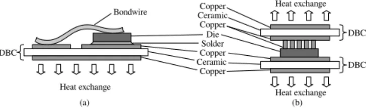
HE VAST MAJORITY of the power modules producedtoday have the structure presented in figure 1(a) (planar structure, [1]): the bottom side of the power semiconductor devices is attached to a ceramic substrate (direct bonded cop-per, DBC), usually using solder, and the top side is connected using wirebonds.Although widely used, this planar structure has some draw-backs. The wirebonds have reliability issues when submitted to thermal cycling [2], and they generate stray inductances in the order of 10 nH [3], causing switching losses and electro-magnetic interferences (EMI). Other limitations of the planar structure include its large surface area (because all electrical interconnects are performed on the same plane, the uppermost copper layer of the DBC substrate), and its limited thermal performance. Indeed, with this structure, the heat dissipated by the power dies is removed through the bottom side only.
As a consequence, many alternative structures have been presented in the recent years. These 3-dimensional (3D) structures offer replacement for the wirebond interconnects. A review of some of the 3D structures is proposed in [4] and [5], but although they present innovative interconnect solutions, most of them still provide cooling through one side of the die only.
3D structures with double-side cooling capability are listed in [6]. Most have a “sandwich” configuration, i.e the dies are sandwiched between two DBC substrates. They differ in the way the dies are bonded to the substrates and in the way they are cooled. Regarding bonding solutions, one can list solder bumps [7], soldered copper cylinders [8], diffusion-bonded copper posts [9], direct soldering [10], or more recently pressure contacts [3].
Among these, we will focus on the “copper posts” structure (Fig. 1(b)). Here, copper posts are electrolytically grown on the surface of the power dies. They are then bonded to the metal layer of a DBC substrate [9]. In this previous study, a layer of tin was used to join the copper elements.
Fig. 1. Power electronics packaging concepts: (a) the planar structure, which is widely used today and (b) a ”3D” concept that allows cooling of the die on both sides.
Recently, we presented a simpler solution to bond two copper parts together: the direct copper-copper bonding pro-cess [11], in which the two parts are simply pressed against each other in vacuum and heated to 200 to 300 °C. This results in a strong bond, without requiring any additional bonding ma-terial. This technique and its application to power electronics packaging as a replacement for soldering are presented below. In this paper, we describe the manufacturing process of a copper-post-based sandwich structure which is assembled using direct bonding only (section III). An electrical test set-up, dedicated to the accurate characterization of the assembly, is presented in section IV. The corresponding results are given in section V, and discussed in section VI.
II. CONCEPT OF THESTRUCTURE
The power module concept developed in the present ar-ticle is shown in Fig. 1(b). A power semiconductor die is inserted between two DBC substrates, allowing cooling from both sides. On the top side of the die, some copper posts provide spacing between the die and the top substrate. This spacing prevents the top substrate from short-circuiting the edge protections of the die.
The posts are also useful to accommodate height differences between dies in a multi-chip power module: different types of dies are commonly used in a single module (such as IGBT and diode, for example), and they do not always have the same thickness. This is not an issue for a “classical” power module (Fig. 1(a)), as it uses wirebonding. In the case of the “sandwich” package (Fig. 1(b)), however, the topside contacts of all the dies must be aligned for proper connection with the top substrate. The copper posts can then compensate for the thickness differences between the dies.
Depending on the form factor of the copper post, they might also offer some mechanical flexibility. This is attractive to manage the differences in coefficient of thermal expansion
(CTE) between various elements of the package. For practical reasons, however, the posts presented in this article have a very low form factor (they are much larger than high), so no flexibility is expected here. Copper posts with a much larger form factor (twice as high as they are large, or more) and with finer pitch (80 µm) have already been presented by other researchers [12].
Another innovative feature of the structure is the solder-free approach: the die (with copper posts) and both DBC sub-strates are bonded together directly, without using any bonding material. The evaluation of the direct bonding technique was described in [11]. It is shown that this technique (described below) offers a very high bonding strength, about half the tensile strength of copper.
Copper posts could be used for both sides of the die or, as described in Fig. 1(b), for one side only. The structure described in this paper has copper posts on one side of the dies only. The backside of the dies (silver) is directly bonded to the polished copper substrate. Both sides of the die are bonded in one step.
III. MANUFACTURING PROCESS
The main step to manufacture the power module from Fig. 1(b) is to electrolytically grow the copper posts on top of the dies. This must be performed at the wafer-level, before the wafer is singulated. In parallel, the copper layer of the substrate must be polished, to facilitate the bonding process. Finally, the three elements (two substrate and one die) are bonded together using a press, in vacuum.
These three steps will now be described in details.
A. Preparation of the dies
Fig. 2 presents the process work-flow required to grow copper posts on dies.
The starting point is a pre-processed wafer, with the power devices already manufactured. This wafer must be removed from the production line just before the dicing step, where it is cut into individual dies.
In our case, the wafer (6 in, 150 mm) was supplied by Microsemi and consists in 6×6 mm2, 600 V, silicon diodes
with an aluminium layer on top, and a silver layer on the back. As we could not process such a large wafer as a whole, we cut it into squares of 25 diodes each (see Fig. 3). In the remaining of this article, the term “wafer” will therefore describe this 25-diode fragment. Please note that the process presented here can be applied to wafers of any size, providing suitable manufacturing equipment is available.
A “seed” layer (25 nm Ti for adhesion, 300 nm Cu) is deposited on top of the wafer by sputtering (Fig. 2(b)) to cover the aluminium layer and the edge terminations of the diodes. This continuous layer is used both to provide a metal surface compatible with the copper posts, and to carry the current for their electrolytic growth.
The wafer is then placed in a custom-designed carrier, and laminated (110 °C) with a patterned copper foil and some thick photosensitive dry film (Dupont Riston PM275, 75 µm-thick [13]) (c). This carrier provides an electric connection to
Wafer Wafer Wafer Wafer carrier Wafer UV Wafer Wafer Wafer Wafer Diode Diode Wafer carrier Wafer carrier Wafer carrier
Diodes wafer with Al top metal Sputtering of Ti/Cu seed layers Mounting of the wafer on carrier, sealing with photosensitive film
Exposure to UV to create micropost pattern
Development of film
Copper electroplating
Extraction from carrier and polishing of Cu excess Stripping of photosensitive film and etching of Ti/Cu seed layers Dicing of wafer (a) (b) (c) (d) (e) (f) (g) (h) (i)
Fig. 2. Process flow of the copper posts manufacturing
"Wafer" (actually cut from a 6 in wafer)
30mm 30mm wiring for electroplating PM 275 Dry film Hot glue Copper foil Wafer carrier
Fig. 3. The wafer fragment (designed here as ”Wafer”) at the beginning of the process, and at step (e) in fig. 2.
the wafer for the electroplating step, as well as sealing from the electroplating bath. In step (d) and (e), the photosensitive layer is exposed and developed (using a 1 wt% solution of Na2CO3) to form molds for the growth of the posts. A
photograph at step (e) is visible in figure 3. Note that the size of the posts (900×900 µm2) was chosen for practical reasons.
With a proper development system (spraying system), much smaller posts are possible, as the nominal resolution of the photosensitive film is 50 µm.
Some wires are then connected to the copper foil (f), and the wafer carrier is immersed in the electroplating bath (220 g/l Cu2SO4, 32 ml/l H2SO4, 0.2 ml/l HCl, 2 ml/l Rubin T200-A,
0 5 10 15 20 25 0 5 10 15 20 25 0 30 60 90 120 150 180 210 240 (a) 0 5 10 15 20 25 0 5 10 15 20 25 0 30 60 90 120 150 180 210 240 (b)
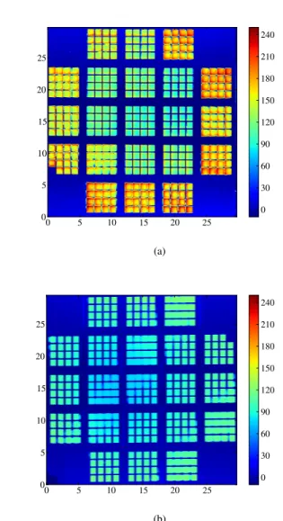
Fig. 4. Topology mapping of the wafer fragment after electroplating (a) and after polishing (b). The color scale is in micrometers, x- and y-axis are in millimeters.
8 ml/l Rubin T200-G and 2 ml/l Rubin T200-E). A copper electrode is placed parallel to the wafer carrier, at 30 mm approximately. The electroplating current (10 mA/cm2) is
supplied by a Keithley 2602A source and measure unit (SMU). The deposition rate at this current level is approximately 12 µm/h.
After 7 h, the wafer carrier is removed from the electro-plating set-up, and the wafer is extracted from the carrier. The top surface is then polished (Logitech PM5, LAAS, Toulouse) to remove the excess copper and to planarize the copper posts (Fig. 2(g)). A mapping, performed on a wafer before and after the polishing using a Dektak 150 profilometer, is visible figure 4. The large differences in height caused by an in-homogeneous current distribution during the electroplating (Fig. 4a) are removed, resulting in a constant post height across the wafer (Fig. 4b).
The photosensitive film is then dissolved in a 3%wt NaOH solution. The seed layers are removed by dipping the wafer in a copper etch solution (Transene APS-100, 1 min), followed by a titanium etch solution (5 % BOE, 1 s) (Fig. 2(h)). Finally, the wafer is singulated using a Disco DAD 3220 dicing saw
(i).
Note that all the steps of this process (sputtering, mask-ing, electroplatmask-ing, polishing etc.) are commonly used in the electronic industry. It could therefore be integrated to the wafer manufacturing. In particular, this would make it directly possible to produce dies with a suitable topside metal finish (copper), instead of depositing Ti/Cu on top of the standard aluminium metallization. The electroplating step takes a long time (7 h), but this does not seem to be incompatible with in-dustrial production, as posts with a comparable height (80 µm) are commonly grown on microelectronic wafers [12].
B. Preparation of the substrates
Direct Bonded Substrates (DBC), from Curamik, are used for this study. To reduce the surface roughness of their copper layers (initial Ra>2 µm) , they are polished, starting with 220-grit SiC paper, down to 1 µm diamond paste and 50 nm silica.
After polishing, the DBC substrates are cleaned in acetone and ethanol, then de-oxidized using a 5 % HF solution, rinsed in de-ionized water and dried using a nitrogen blow nozzle. Once the substrates cleaned, the assembly process is performed immediately (within one hour) to avoid re-oxidation of the copper.
C. Assembly process
The direct bonding process, used here to assemble the sandwich package, is investigated in details in [11]. Basically, it consists in pressing the elements to be bonded together, and to heat them up to a given temperature (here from 200 and 300 °C), using a special pressing tool (a so-called Spark Plasma Sintering –SPS– press). It is comparable to a thermo-compression, but the bonding strength was found to be much higher than previously reported, with tensile strengths measured at up to 261 MPa (to be compared with 365 MPa for a bulk copper sample).
For the results presented here, due to equipment availability, two bonding tools are used: the same SPS press as used in [11] (FCT Systems HP D25/1), and a Rapid Thermal Annealing (RTA) furnace, equipped with a pressing fixture (Jipelec Jetfirst 100). Both systems allow bonding in vacuum, with very fast heat-up ramps. The main difference are the heating system (Joule heating for the SPS, halogen lamps for the RTA), and the pressing force (5 kN for the SPS, 0.26 kN for the RTA). In the SPS, a custom graphite jig [14] is used to reduce the actual force applied to the assemblies, and to avoid damaging the dies with an excessive force. As a consequence of using this jig, the actual force applied to the assemblies processed with the SPS could not be measured.
The bonding is performed using the following parameters: heat-up ramp 100 °C/min, bonding time 5 min, bonding temperature 200 or 300 °C. The whole bonding process takes place in vacuum.
1) Preliminary electrical test: prior and after assembly, the diodes are electrically controlled to detect any damage that could be caused by the packaging process. In both cases, we use a Keithley 2410 SMU connected to a probe station (with
TABLE I
SHEAR TEST MEASUREMENTS PERFORMED ON SANDWICH STRUCTURES BONDED USINGSPSANDRTA. FIS THE SHEAR FORCE, STHE TOTAL CONTACT SURFACE OF THECU POSTS/SUBSTRATE INTERFACE,ANDτIS
THE CORRESPONDING SHEAR STRENGTH.
SPS RTA T F S τ T F S τ (°C) (N) (mm2) (MPa) (°C) (N) (mm2) (MPa) 300 113 2.6 43 300 199 11.8 16 300 184 8.9 20 300 93 7.3 12 300 275 8.4 32 200 133 5.2 25 300 275 8.9 30 200 187 4.0 46 200 181 7.0 25 200 21 1.1 18 200 31.5 5.6 5.6 200 176.5 8.4 21
Fig. 5. Fracture surface after a shear test: most copper posts were separated from the die (left) and stayed on the substrate (right). In some cases (bottom right post on the die), the fracture occurred in the silicon, indicating a good bond quality.
a 4-probe configuration). Forward and reverse characteristic are performed, but with limited forward current (1 A, limited by the SMU and the probes) and reverse voltage (limited to -300 V to prevent arcing in air).
After packaging, all diodes show a small improvement of their forward characteristic (about 60 mV lower forward voltage at 1 A current as compared to the diodes with the electroplated posts), and no change of the reverse current (in the order of 30 nA at 300 V). The improvement of the forward characteristic can be attributed to the test conditions: prior to the assembly, the probes are connected to one copper post only, hence injecting the current in a localized manner. After assembly, the probes are connected to the inner copper layer of the DBC substrate, which spreads the current among all copper posts.
2) Mechanical testing of the assembly: In [11], the bonding tests were performed on bulk copper rods only. In order to make sure that the direct bonding technique worked on more complex systems, 12 sandwich structures are assembled and mechanically tested (shear test). The results are visible in table I, with T being the assembly temperature, F the force required to separate the top substrate from the die, S the surface of the interface between the copper posts and the top substrate, and τ = F/S the corresponding shear strength. The surface S was obtained by summing the surface of the posts that remained on the top substrate and the surface of the imprints left by the posts in the top substrate (when the failure occurred at the post/substrate interface). Although the copper
Die Die Micropost Upper DBC Lower DBC 100µm 300µm
Fig. 6. Cross-section of a DBC/diode/DBC assembly. The diode has micro-posts on top.
posts and the substrate are polished prior to assembly to ensure good contact, the surface S is found to be significantly smaller than expected for all samples: the expected value is 13 mm2
(16 posts with a 900×900 mm2 surface), while the measured
values range from 1.1 up to 11.8 mm2.
Several failure modes can be observed after shear test. As an example, on Fig. 5, only 2 out of 16 posts remain on the die. The other 14 separated from the die either at the seed layer interface, or even within the silicon. The bottom left post on the substrate in Fig. 5 shows fragments of silicon. On the other samples (not shown here), the same failure modes can be observed, albeit in different proportions (more or less posts remaining on the die, from small cracks in the silicon up to complete destruction of the die).
Given the small sample count, no significant effect can be found regarding the bonding equipment (SPS or RTA) and the bonding temperature (200 and 300 °C). The average shear strength is 24.5 MPa (with 11.9 MPa standard deviation). In comparison, the MIL-STD 883 requires minimum shear strength values always smaller than ≈ 6 MPa [15] (exact value depends on die size). This standard cannot be applied directly here, as it is intended for plain die attaches, not for posts, but it indicates that the values listed in table I are realistic for the application. Note that some assemblies were attempted using a non-polished DBC substrate, but they all showed a poor adhesion (around 20 N), with all assemblies failing at the post/substrate interface.
The cross-section of another assembly is visible in figure 6. The interface between the copper posts and the upper DBC is barely visible.
IV. ELECTRICAL CHARACTERIZATION SET-UP
Thanks to its copper posts, the packaging solution presented in this paper is expected to offer a very low resistance com-pared to aluminium wirebonds. The copper posts are indeed shorter, wider, and copper is a better electrical conductor than aluminium.
As a consequence, we designed a specific characterization set-up to perform accurate forward I(V) characterization up to 200 A. It is described in this section, while the measurement results are presented in section V.
(a) Bottom side (b) Top side
30 mm
30 mm 6 mm
6 mm
(c) Cross-section of the assembly
Die Microposts Substrates
Access to
top Cu layer pad (polished)protuding Cu
Fig. 7. Layout of the DBC substrates (a) and (b), and cross-section of the assembly (c).
A. Test vehicles
Two different packages are investigated, both containing the same chip model: TO-247 plastic packages (Microsemi, reference APT60D60BG) and a sandwich package made using the process described in section III, with a design described below.
1) TO-247 plastic package: For their characterization, the diodes are attached to a cold plate which is connected to a chiller to control the ambient temperature. Kelvin (4-wire) connections are attached to the leads of the package, as close as possible to the epoxy molding. This configuration minimizes the effect of the leads in the I(V) characterization, but does not cancel-out the resistance caused by the internal elements of the package, especially the wirebonds.
2) Sandwich package with Kelvin contacts: This package (see drawings in Fig. 7 and corresponding photograph in Fig. 8) is designed to allow voltage measurement at various places, to detect possible current balancing issues that might be caused by improper bonding of the posts. Some holes are laser-drilled in the ceramic layer (see Fig. 7(c)) for current injection. Their location, directly above and below the die, is chosen to homogenize the current distribution.
A two-step copper etching technique is used to form a pedestal on the inner surfaces of the substrate. This protruding part is used as an alignment feature to position the die during the assembly. It also simplifies the polishing step of the substrates (section III-B): only the surface directly involved in the bonding need to be polished, not the entire surface of the substrate.
Finally, a graphite jig is used to align both substrates during the assembly. The bonding is performed using the RTA
Fig. 8. The test vehicle (≈ 30×30 mm2), with two identical DBC substrates
around a diode (not visible).
Test support Spring probes for current injection
Shunt Kelvin connections for voltage measurement
Fig. 9. Photograph of the test bench, with a test support for the power module. The electric circuit is kept compact to reduce stray inductances and to allow short power pulses.
furnace.
B. Test equipment
A photograph of the pulsed characterization system is visible in Fig. 9 (with a test support designed for the sand-wich package). The current is supplied by a power source (Xantrex XDC 20V-300A) in series with an inductor. A set of power transistors is used to shunt the power source, and to periodically divert the current to the test vehicle. A T&M research aselfic shunt (W-2-005-2FC 0.005072 Ω) is used to measure the current with accuracy and short response time. Note that the commutation loop is kept as compact as possible, to minimize the stray inductances. Overall, this system allows
0.6 0.8 1.0 1.2 1.4 1.6 1.8 2.0 Forward Voltage [V] 0 50 100 150 200 Forw ard Current [A] To 247 Sandwich package
Fig. 10. Direct I/V characteristic for diodes packaged respectively in a T0-247 plastic package, and in the proposed “sandwich” package. Measurements performed at 20°C.
the measurement with pulses shorter than 10 µs and with current levels up to 300 A.
V. EXPERIMENTALRESULTS
The forward I(V) characterizations performed using the set-up described in section IV is visible in figure 10. Five diodes are used, two in a TO-247 package, and three in a sandwich package.
Contrarily to what was expected, the TO-247-packaged diodes offer a lower voltage drop than those in the sandwich packages (200 mV lower for a 200 A forward current). Al-though all 5 diodes satisfy the specifications in the APT60D60 datasheet (typical values: 1.6 V for 60 A, 1.9 V for 120 A), the relatively higher resistance of the sandwich package is surprising. For the bonding study presented in [11], the elec-trical resistance of the bonding interface was so small that we were not able to measure it with our test setup (limited to a resolution of 100 µΩ.mm2).
VI. DISCUSSION
Part of the difference could be attributed to the diodes dies themselves: the dies used in the sandwich and the T0-247 package were probably not manufactured at the same time, and therefore could exhibit differences in characteristics.
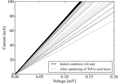
Another explanation is related to the Ti/Cu metallization that is deposited to allow the growth of the copper posts (Fig. 2(b)). Surface (square) resistance measurement measured with a 4-probe set-up (aligned with a 1-mm pitch) are visible in Fig. 11. The plain lines correspond to the 25 diodes of an un-processed wafer fragment, and show little dispersion. The dotted lines correspond to the 25 diodes of a fragment of the same wafer, after the Ti/Cu metallization. Not only is the voltage-drop higher, but the dispersion is also much larger. Identical measurements (not presented in Fig. 11) show that after chemically removing the Ti/Cu metallization, the surface resistance returns to its original value (plain lines in Fig. 11), which proves that the aluminium layer is not affected.
0.00 0.05 0.10 0.15 0.20 Voltage [mV] 0 20 40 60 80 100 Current [mA]
Initial condition (Al top)
After sputtering of Ti/Cu seed layer
Fig. 11. square resistance measurement performed on the topside metalliza-tion of dies in the initial condimetalliza-tion (aluminium) and after sputtering of the seed layer (Ti/Cu on top of the aluminium).
200 300 400 500 600 700 800 Sputter time [s] 0 2 4 6 8 10 12 14 Intensity (x1000) Cu2 Al2 02 Ti Al2 AlO2 TiO CuO Cu2
Fig. 12. SIMS profiles performed on the same wafer as Fig. 11. Metals are plotted with a plain line (Titanium is barely visible, with a small bump over the 500 s mark), and the oxides with dotted lines. It appears that there is a highly oxidized interface between Al and Ti, and that most of the Ti layer is oxidized.
If the consequence of this higher surface resistance is obviously an increase in the series (vertical) resistance of the diode, it is difficult to actually calculate it: we do not know which element of the Ti/Cu actually causes the increase in resistivity (is it at the interface between aluminium and titanium? in the titanium or copper layer themselves?, at the Ti/Cu interface?). Furthermore, the equations used to find out the resistivity of a material from surface resistance measurement were developed for a conductive layer on a isolating (or semi-isolating) substrate. In our case, the layer that needs characterization (Ti/Cu) is attached to a thicker conducting layer (aluminium).
From the process notes, it appears that a pressure change (increase from 3.10−6mbar to 6.10−5 mbar) was observed in
or the degassing of the chamber). This might have caused the oxidation of the Ti layer, and resulted in a higher resistivity of this layer. This is confirmed by SIMS (Secondary Ions Mass Spectroscopy, ) measurements performed (“Science et Surface, Ecully, France) on the same wafer as in Fig. 11 (see Fig. 12). It appears that the Ti/Al interface is strongly oxidized. Such measurements were performed for two diodes of the wafer, the best and the worst diodes from Fig. 11, but the SIMS profiles are identical.
As stated before, the Ti/Cu metallization is required in our process to enable copper electroplating on the standard aluminium finish of the diodes. In an industrial process, this would not be necessary as the diodes would be directly manufactured with a suitable topside metal. Power devices with a thick copper metal layer have recently been intro-duced [16], and would probably be well-suited to copper posts interconnects.
VII. CONCLUSION
A power module sandwich structure, based on copper-to-copper direct bonding has been presented in this article. Compared to existing solutions, no additional bonding material (solder or adhesive) is required.
The whole manufacturing process has been presented in de-tails and demonstrated on a diode wafer. Several modules have been assembled and show an acceptable bonding strength. One advantage of this process is that most of the manufacturing steps take place on the wafer, before singulation (“wafer-scale packaging”), so many dies can be processed at the same time. A dedicated characterization set-up has been developed, including specific DBC substrates and a test bench generating short current pulses.
Using this set-up, it was found that the resistance introduced by the sandwich packaging is slightly higher than that of a conventional TO-247 package. An hypothesis is that this disappointing result can be attributed to the poor quality of the Ti/Cu seed layer used for the electroplating of the copper posts.
If the copper posts were to be implemented in an industrial process, it would be part of the diodes manufacturing process, and the Ti/Cu metallization would not be required. Therefore, we consider that the higher resistance of the sandwich package as compared to the TO-247 is not an intrinsic problem of the proposed packaging solution.
ACKNOWLEDGMENT
The authors would like to thank M. Dupin, from Microsemi, and M. Trinel, from Richardson RFPD France, for supplying the diodes used in this study and the Agence Nationale de Recherche (ANR) for its support of this work through the grant “ECLIPSE”. Some of the manufacturing steps were performed on the 3DPHI platform.
REFERENCES
[1] W. W. Sheng and R. P. Colino, Power Electronic Modules: Design and Manufacture, 1st ed. CRC, jun 2004.
[2] M. Ciappa, “Selected failure mechanisms of modern power modules,” Microelectronics Reliability, vol. 42, no. 4-5, pp. 653 – 667, 2002. [Online]. Available: http://www.sciencedirect.com/science/article/ B6V47-45CN6JG-8/2/9bab07a93f785fbcee637106dbe0ff07
[3] E. Vagnon, P.-O. Jeannin, Y. Avenas, J. Cr´ebier, and K. Gu´epratte, “A Busbar Like Power Module Based On 3D Chip On Chip Hybrid Integration,” in Applied Power Electronics Conference and Exposition, 2009. APEC 2009. Twenty-Fourth Annual IEEE. IEEE, 2009, pp. 2072–2078. [Online]. Available: http://hal.archives-ouvertes.fr/docs/00/ 39/68/84/PDF/Vagnon APEC.pdf
[4] L. M´enager, C. Martin, B. Allard, and V. Bley, “Industrial and lab-scale power module technologies : A review,” in Proceedings of the 32nd Annual Conference of the IEEE Industrial Electronics Society (IECON), IEEE, Ed., Paris, France, nov 2006.
[5] J. Calata, J. G. Bai, X. Liu, S. Wen, and G.-Q. Lu, “Three-Dimensional Packaging for Power Semiconductor Devices and Modules,” Advanced Packaging, IEEE Transactions on, vol. 28, no. 3, pp. 404–412, 2005. [6] J. Schulz-Harder, “Review on Highly Integrated Solutions for Power
Electronic Devices,” in Proceedings of the Conference on Integrated Power electronics Systems (CIPS), N¨uremberg, mar 2008, p. 7 p. [Online]. Available: http://www.electrovac.com/sprache2/n221666/n. html
[7] C. Gillot, C. Schaeffer, C. Massit, and L. Meysenc, “Double-Sided Cooling for High Power IGBT Modules Using Flip Chip Technology,” IEEE Transaction on Components and Packaging Technology, vol. 24, no. 4, pp. 698–704, dec 2001.
[8] P. Solomalala, J. Saiz, A. Lafosse, M. Mermet-Guyennet, A. Castellazzi, X. Chauffieur, and J.-P. Fredin, “Multi-domain simulation platform for virtual prototyping of integrated power systems.” in Power Electronics and Applications, 2007 European Conference on, sept. 2007, pp. 1 –10. [9] L. M´enager, M. Soueidan, B. Allard, V. Bley, and B. Schlegel, “A Lab-Scale Alternative Interconnection Solution of Semiconductor Dice Compatible with Power Modules 3D Integration,” IEEE Transactions on Power Electronics, vol. 25, no. 7, pp. 1667–1670, jul 2010.
[10] C. Buttay, J. Rashid, C. Johnson, F. Udrea, G. Amaratunga, P. Ireland, and R. Malhan, “Compact Inverter Designed for High-Temperature Operation,” in Proc. IEEE Power Electronics Specialists Conference PESC 2007, 2007, pp. 2241–2247.
[11] B. Mouawad, M. Soueidan, D. Fabr`egue, C. Buttay, B. Allard, V. Bley, H. Morel, and C. Martin, “Application of the Spark Plasma Sintering Technique to Low-Temperature Copper Bonding,” IEEE Transactions on Components, Packaging and Manufacturing Technology, vol. 2, no. 4, pp. 553–560, apr 2012, early Access.
[12] J. Kloeser and E.-A. Weissbach, “high performance flip-chip packages with copper pillar bumping,” Global SMT and Packaging, article, may 2006. [Online]. Available: http://www.trafalgar2.com/documents/ Technical Articles/6.5-kloeser.pdf
[13] DuPont, “PlateMaster PM200 Series: Data Sheet & Processing Infor-mation,” DuPont, Tech. Rep.
[14] B. Mouawad, C. Buttay, M. Soueidan, H. Morel, and B. Al-lard, “3-Dimensional, Solder-Free Interconnect Technology for High-Performance Power Modules,” in Proceedings of the Conference on Integrated Power Systems (CIPS), N¨uremberg, 2012.
[15] Test Method Standard Microcircuits, MIL-STD-883G Std., feb 2006. [16] K. Guth, D. Siepe, J. G¨orlich, H. Torwesten, R. Roth, F. Hille, and
F. Umbach, “New assembly and interconnects beyond sintering meth-ods,” in Proceedings of PCIM, Nuremberg, may 2010, pp. 232–237.
Bassem Mouawadreceived the Ph.D. degree from ”Institut National des Sciences Appliqu´es” (INSA) in Lyon, France, in 2013. He was then a research fellow in MATEIS Laboratory (INSA Lyon) where his research was mainly focused on the elaboration of materials by the means of flash sintering/bonding as well as on the mechanical properties of metallic alloys. In 2014, he joined the Power Electronics Machines and Control (PEMC) group at the Univer-sity of Nottingham, in Nottingham, United Kingdom where he is currently a research fellow. His current research interests include packaging technologies for SiC devices.
Benoit Thollinreceived the Ph.D. degree in Elec-trical Engineering from the University of Greno-ble, France, in 2013. After post-doctoral researches in the Grenoble Electrical Engineering Laboratory (G2Elab), focusing on thermal management and thermal characterization of power semiconductor devices, he currently works as a researcher in the French Alternative Energies and Atomic Energy Commission (CEA). His field of research is on high temperature power components packaging.
Cyril Buttay (M’04) received the Engineer and Ph.D. degrees from the “Institut des Sciences Ap-pliqu´ees” (INSA) in Lyon, France, in 2001 and 2004 respectively. From 2005 to 2007 he was a research associate within the Electrical Machines and Drives research team of the University of Sheffield (UK) and the Power Electronics Machines and Control group of the university of Nottingham. Since 2008, he has been a scientist with the French Centre Na-tional de Recherche Scientifique (CNRS), working within the laboratoire Amp`ere, Lyon, France on high-temperature power electronics, with a special focus on packaging-related issues.
Laurent dupont received the Electrical Engineer in 2002, and the Ph.D. degree in electrical en-gineering from the ´Ecole Normale Sup´erieure de Cachan, Cachan, France, in 2006. After ten years of experiences in industry, he works as researcher scientist in the Laboratory of New Technologies in the French research institute IFSTTAR, Versailles, France since 2007. His research interests are geared towards the evaluation of power semiconductor mod-ules robustness. The research activities are especially focused about parameters which allow estimations of the temperatures and the ageing indicators of power components in operative conditions.
Vincent Bley was born in Castelsarrasin, France in 1971. He obtained his M.Sc. degree in electri-cal engineering from Paul Sabatier University of Toulouse in 1995. He received his PhD in 2000 whose subject was about protections integration in power electronics modules (ZnO varistors, BaTiO3 based capacitors...). Since 2001, he is associate Professor, his research activity is focussed on a set of technological process from materials to functions and their electrical characteristics with the aim to integrate passives and actives functions in hybrid power electronics applications. Currently, he is in charge of the development of the CNRS national technological platform 3DPHI (Three-Dimensional Power Hybrid Integration).
Damien Fabr`egue is an associate professor, MATEIS lab, Materials Science and Engineering de-partment, INSA Lyon. His research activities are fo-cused on elaboration and optimization of metallic al-loys (steels, aluminum, titanium, cobalt, copper,. . . ) in terms of microstructure and mechanical properties through rapid thermo mechanical treatments. These activities are going from flash sintering/bonding of metals and architectured materials to the change of the microstructure by complex thermo mechanical processes (welding, deformation at high tempera-ture,. . . )
Maher Soueidanreceived the Ph.D. Degrees from the ”Universit´e Lyon 1” in Lyon, France in 2006. He joined the CNRS, the National Center for Scientific Research in 2010. He is currently with the AMPERE Laboratory, center for Electrical Engineering in the ”Institut des sciences Appliqu´ees” (INSA) in Lyon. His reaserch interests include materials science for power semiconductor devices, power system mod-ules, physico-chemical characterization and power module packaging and reliability.
Benoˆıt Schlegel was born in St Avold, France in 1972. After working in the field of microelectronics industry, he joined the CNRS in 2002. Attached to the LAPLACE as engineer assistant, he is in charge of samples preparations and technological processes optimization.
Julien Pezard was born in 1987. He received the Engineer degree from the Ecole Normale Sup´erieure d’ing´enieurs of Caen (ENSICAEN) and the M.Sc degree from the university of Caen (UNICAEN) in 2012. He is now working as a Ph.D student at the Ecole Centrale of Lyon,in the AMPERE labora-tory. His research interests regroup Material physics, microelectronic devices development on multiple substrates,but also chemistry, electrochemistry, and biology for the elaboration of microbiosensors.
Jean-Christophe Crebieris a CNRS senior scien-tist in the fields of integrated power electronics. He earned his Bachelor and Masters Degrees in Elec-trical Engineering in 1995. In 1999, he received his PhD in Power Electronics, EMC for PFC converters from INPG, France. In 2000 he was working as a Post-Doc student in CPES (Center for Power Elec-tronics Systems), USA, doing research in system integration. Since 2001, he is with G2ELab-CNRS (National Center for Scientific Research), France, as a full time researcher. His research fields are system and functional, hybrid and monolithic semiconductor integration for power active devices and converters.