RESEARCH OUTPUTS / RÉSULTATS DE RECHERCHE
Author(s) - Auteur(s) :
Publication date - Date de publication :
Permanent link - Permalien :
Rights / License - Licence de droit d’auteur :
Dépôt Institutionnel - Portail de la Recherche
researchportal.unamur.be
University of Namur
Temperature dependence of charge localization in high-mobility, solution-crystallized
small molecule semiconductors studied by charge modulation spectroscopy
Meneau, Aurélie Y.B.; Olivier, Yoann; Backlund, Tomas; James, Mark; Breiby, Dag Werner;
Andreasen, Jens Wenzel; Sirringhaus, Henning
Published in:
Advanced functional materials
DOI:
10.1002/adfm.201502502
Publication date:
2016
Document Version
Publisher's PDF, also known as Version of record
Link to publication
Citation for pulished version (HARVARD):
Meneau, AYB, Olivier, Y, Backlund, T, James, M, Breiby, DW, Andreasen, JW & Sirringhaus, H 2016,
'Temperature dependence of charge localization in high-mobility, solution-crystallized small molecule
semiconductors studied by charge modulation spectroscopy', Advanced functional materials, vol. 26, no. 14, pp.
2326-2333. https://doi.org/10.1002/adfm.201502502
General rights
Copyright and moral rights for the publications made accessible in the public portal are retained by the authors and/or other copyright owners and it is a condition of accessing publications that users recognise and abide by the legal requirements associated with these rights. • Users may download and print one copy of any publication from the public portal for the purpose of private study or research. • You may not further distribute the material or use it for any profit-making activity or commercial gain
• You may freely distribute the URL identifying the publication in the public portal ?
Take down policy
If you believe that this document breaches copyright please contact us providing details, and we will remove access to the work immediately and investigate your claim.
FULL P
APER
in the transfer integrals large enough to dynamically localize charge carriers. [ 4–6 ] The model is able to explain the puzzling dichotomy associated with the observation of both band-like transport characteristics, such as a free-electron Hall effect, and signatures of carrier localization, such as a pronounced molecular charge-induced absorption in charge modulation spec-troscopy (CMS) in several, high mobility molecular semiconductors. [ 7,8 ] Supported by theoretical calculations and dynamic molecular simulations, Chang et al. high-lighted the role of crystal packing as they demonstrated that 2D6,13bistriisopropylsilylethynyl pentacene (TIPSP) is signifi -cantly more affected by dynamic disorder than is 1,4,8,11-tetramethyl-6,13-triethyl-silylethynyl pentacene (TMTES-P). In TIPS-P charge carriers at the Fermi level are expected to be less delocalized than in TMTES-P, which explains the nonideal Hall response and generally lower mobilities observed for TIPS-P.
Unfortunately, it has not been possible to date to study experi-mentally the intrinsic temperature dependence of transport in a dynamic disorder dominated system. Although in some systems a band-like temperature dependence, i.e., mobility decreasing with increasing temperature, has been observed in a tempera-ture range between 200 and 300 K, [ 9–12 ] at lower temperature the mobility is typically exhibiting a temperature-activated behavior. This is generally interpreted as a manifestation of shallow trap states, but the nature of these trap states is not understood in
Temperature Dependence of Charge Localization in
High-Mobility, Solution-Crystallized Small Molecule
Semiconductors Studied by Charge Modulation Spectroscopy
Aurélie Y. B. Meneau , Yoann Olivier , Tomas Backlund , Mark James , Dag Werner Breiby ,
Jens Wenzel Andreasen , and Henning Sirringhaus *
In solution-processable small molecule semiconductors, the extent of charge carrier wavefunction localization induced by dynamic disorder can be probed spectroscopically as a function of temperature using charge modulation spectroscopy (CMS). Here, it is shown based on combined fi eld-effect tran-sistor and CMS measurements as a function of temperature that in certain molecular semiconductors, such as solution-processible pentacene, charge carriers become trapped at low temperatures in environments in which the charges become highly localized on individual molecules, while in some other molecules the charge carrier wavefunction can retain a degree of delocalization similar to what is present at room temperature. The experimental approach sheds new insight into the nature of shallow charge traps in these materials and allows identifying molecular systems in which intrinsic transport proper-ties could, in principle, be observed at low temperatures if other transport bottlenecks associated with grain boundaries or contacts could be removed.
DOI: 10.1002/adfm.201502502
1. Introduction
Much has been learnt on the structure–activity relationship between molecular structure, solid-state ordering, and charge carrier mobility in high-mobility, molecular semiconductors over the last few decades and a variety of transport models have been proposed. [ 1–3 ] The dynamic disorder model provides a solid framework for understanding the temperature-dependent charge carrier and transport properties on a molecular level. It assumes that even in the crystal phase, the extreme sensitivity of neighboring molecular orbitals to small nuclear displace-ments as a result of thermal fl uctuations produces variations Dr. A. Y. B. Meneau, [+] Dr. Y. Olivier, [++] Prof. H. Sirringhaus
Cavendish Laboratory, University of Cambridge Cambridge CB3 OHE , UK
E-mail: [email protected] Dr. T. Backlund, Dr. M. James Merck Chemicals Ltd. Chilworth Technical Center University Parkway
Southampton SO16 7DQ , UK Prof. D. W. Breiby
Department of Physics
Norwegian University of Science and Technology (NTNU)
Høgskoleringen 5 7491 Trondheim , Norway
Dr. J. W. Andreasen
Department of Energy Conversion and Storage Technical University of Denmark
Frederiksborgvej 399 Building 111
4000 Roskilde , Denmark
[+] Present address: Merck Chemicals Ltd, Chilworth Technical Center,
University Parkway, Southampton SO16 7DQ, UK
[++] Present address: Laboratory for Chemistry of Novel Materials,
Université de Mons, 20 Place du Parc, 7000 Mons, Belgium
APER
most systems. They could be due to structural point defects or chemical impurities present in the bulk of crystalline grains, states associated with grain boundaries [ 13 ] or states localized at the semiconductor–dielectric interface. [ 14–16 ] Identifi cation of their origin is challenging as few spectroscopic probes exist that are able to detect interfacial trapped charge species at concentra-tions typically less than 10 12 per cm 2 . CMS provides a powerful spectroscopic technique to study the nature of such shallow trap states. As long as the shallow trap states can be fi lled and emp-tied on the time scale of the modulation of the charge carrier concentration in the accumulation layer of a fi eld-effect tran-sistor (FET) by an applied gate voltage, CMS provides spectro-scopic information about the nature of the associated charge carriers as a function of temperature which can be directly correlated with the measured temperature dependence of the fi eld-effect mobility. For example, in TIPS-P Sakanoue et al. [ 11 ] observed a sharpening of the charge-induced absorption CMS signature at low temperature, in the same temperature regime in which the mobility became thermally activated. This was interpreted in terms of a shallow trap state in which the charge carrier wavefunction becomes localized onto a single TIPS-P molecule. As a direct fi ngerprint of the degree of localization sensed by mobile charges in the FET accumulation layer the CMS spectra at low temperature as compared to the room tem-perature spectra may contain key information about the trap-ping mechanisms in particular materials systems.
Here we present the results of a CMS/temperature-dependent mobility study comparing TIPS-P and TMTES-P to other high-mobility solution-processable acenes, including another soluble pentacene derivative, 2,3,9,10-tetramethyl-6,13-triisopropylsily-lethynyl-pentacene (β-TMTIPS-P) and 2,8-difl uoro-5,11-triethylsily-lethynyl-anthradithiophene (diF-TES-ADT) ( Figure 1 ), that is one of the most widely studied, highest mobility, solution processable heteroatom acene derivatives. In single crystals the former packs into strongly interacting, cofacial 1D structures (Figure S1, Sup-porting Information), whilst the latter is known for its 2D-brick-wall packing. [ 17 ] We observe signifi cant differences between these molecules in the degree of charge carrier wavefunction localiza-tion in the trap-dominated regime at low temperature that leads us to conclude that the nature of shallow traps in these systems is not universal but may be different from system to system.
2. Results
We fi rst measured, for each compound, the temperature dependence of the mobility in the top-gate, bottom-contact FET architecture. We grew polycrystalline (single component)
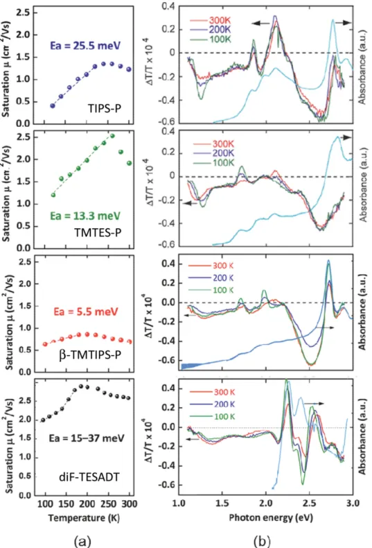
thin fi lms by spin-coating on top of pentafl uorobenzenethiol-treated Au source-drain electrodes and selected Cytop, a per-fl uorinated, low k-polymer as the gate dielectric to reduce charge trapping at the gate insulator/semiconductor inter-face. All molecules gave good p-channel FET characteristics in 20 µm channel devices, with room-temperature mobilities of 0.7 cm 2 V −1 s −1 (β-TMTIPS-P), 1.2 cm 2 V −1 s −1 (TIPS-P), 1.9 cm 2 V −1 s −1 (TMTES-P), and 2.5 cm 2 V −1 s −1 (diF-TES-ADT). At relatively high drain voltage, V D = −40 V, in TIPS-P we found the absolute current and the slope of the saturated transfer characteristics, i.e., the extracted effective mobility, to increase monotonically with decreasing temperature in the temperature range 240 K < T < 300 K, before dropping upon further cooling, in line with previous reports [ 11 ] In fact, we measured a negative temperature coeffi cient of the mobility for all four compounds, even for β-TMTIPS-P ( Figure 2 a) with its room-temperature mobility well below the Mott–Ioffe–Regel limit, which requires the mobility µ to be larger than µ > e a 2 W /( h¯ k
B T ) for a band-transport description to be valid. Here a is the lattice constant and W is the estimated bandwidth (assumed to be typically on the order of 100 meV). Regardless of their starting (room tem-perature) performance, all molecules were found to share a sim-ilar electrical behavior at low temperature too, as past a pivotal temperature all mobilities become thermally assisted, i.e., the transport becomes trap limited. The differences lie in the value of the cross-over temperatures (associated with trap density) and in the activation energies E a extracted from an exponential fi t of the mobility in the trap-limited low-temperature transport regime. In TIPS-P we calculated characteristic activation ener-gies >25 meV; that is equivalent to a trap depth around fi ve times deeper than that in β-TMTIPS-P ( E a ≈ 6 meV). TMTES-P was found to sit in the middle of TITMTES-PS-TMTES-P and β-TMTITMTES-PS-TMTES-P, with E a ≈ 13 meV. In diF-TES-ADT a more complex temperature dependence of the mobility was observed with a narrow tem-perature range between 150 and 200 K, where a relatively high activation energy of ≈37 meV could be extracted and a regime below 150 K with a smaller activation energy of ≈15 meV. We measured three samples prepared under identical conditions and observed only small variations in the value of these activa-tion energies (<5 meV).
In light of these subtle differences we then measured the CMS spectra of all molecules as a function of temperature, following the methodology described in ref. [ 11 ] . Typically, a negative DC bias was applied to a semitransparent FET fabri-cated in a top-gate confi guration, optimized to remove any arti-facts in the measurement. This allowed probing of positively charged carriers in the semiconductor that are attracted to the Figure 1. Chemical structure of the semiconducting small molecules compared in this study: a) TIPS-P, b) TMTES-P, c) β -TMTIPS-P, and d) diF-TES-ADT.
FULL P
APER
interface with the dielectric. If charge injection is accompanied by structural reorganization of the molecules and the forma-tion of polaronic levels within the semiconductor gap, new optical transitions below the π−π* absorption can be detected as a weak modulation of the transmission spectrum. In all
molecules studied here we observe at broad, subgap charge-induced absorption between 1.1 and 2 eV, that is also observed in rubrene single crystals studied in ref. [ 11 ] . This is evidence of the molecular reorganization associated with the localized nature of the charge carriers in these materials leading to
www.MaterialsViews.com
Figure 2. a) Temperature-dependent saturation mobility ( V D = −40 V) measured in 20 µm channel (from top to bottom) TIPS-P, TMTES-P, β-TMTIPS-P,
and diF-TES-ADT FETs, with top-gate architecture and ≈470 nm thick Cytop dielectric. The activation energies ( E a ) extracted in the trap-dominated
regimes (dashed lines) are also given. b) Temperature-dependent differential transmission CMS spectrum of (from top to bottom) TIPS-P, TMTES-P, β-TMTIPS-P, and diF-TES-ADT transistors. The light blue curves are the respective thin-fi lm absorption spectra. TIPS-P and TMTES-P spectra were extracted with permission from Ref. [ 11 ] .
APER
characteristic charge-induced absorption different from that of the neutral molecule. The spectra for TIPS-P were obtained from a material batch from a different supplier than that used in Sakanoue’s work and were found to be very similar to those shown in ref. [ 11 ] exhibiting a broad charge-induced absorption with Δ T / T < 0 between 1.1 and 2 eV that sharpens into a band centered ≈1.25 eV at low temperatures (Figures 2 b and 4 a), the shape of which is very similar to that of the isolated radical cation in solution (Figure S2, Supporting Information). This suggests that the observed localization of charges that is evident in the sharpening of the polaron absorption band is not related to specifi c, supplier-dependent chemical impurities.
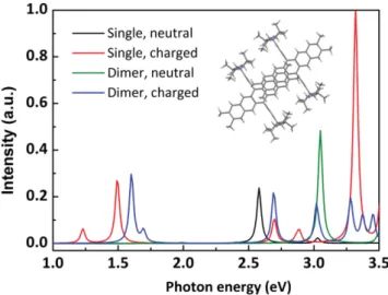
We established the room temperature spectrum of β-TMTIPS-P (Figure 2 b) to be qualitatively similar to that of TIPS-P and TMTES-P. We detected a broad, low-energy charge-induced absorption ≈1.2–1.5 eV, and a higher-lying transition at 2.5–2.6 eV which resemble those found in TIPS-P, only slightly redshifted. Taking into account errors in estimating transition energies in the gas phase, these are reasonably well predicted by quantum-chemical calculations performed on singly charged, isolated β-TMTIPS-P molecules and dimers ( Figure 3 ). Such cal-culations were also performed for the other molecules, for which similar results were obtained. The position of the cation-induced absorptions ≈1.5 and 3.5 eV in the simulated spectra is different between the monomer and the dimer, which demonstrates that the peak position varies depending on the degree of charge delo-calization. In fact, our interpretation of the broad cation-induced absorption observed at room temperature within the dynamic disorder framework is that the spectra are broadened by sta-tistical averaging over molecular confi gurations in which the charge is delocalized over a different number of molecules as a result of thermal lattice fl uctuations. [ 8 ] The optical absorption of a photon is an ultrafast process occurring on a timescale on which the thermal lattice fl uctuations responsible for dynamic disorder are effectively frozen and the ensemble of charge car-riers present in the accumulation layer of the FET is expected to comprise a statistical distribution of confi gurations with dif-ferent degrees of charge delocalization, each of which absorbs at a different wavelength. The difference between β-TMTIPS-P and TIPS-P at 300 K is that in the former we detected a sig-nifi cantly smaller, net Δ T / T > 0 signal for the bleaching of the neutral highest occupied molecular orbital–lowest unoccupied molecular orbital (HOMO–LUMO) transition ≈1.7–2.0 eV, but a considerably stronger signal for the higher-lying bleaching signal ≈2.7 eV. The vibronic transitions, which are clearly visible at 1.71, 1.87, and 1.98 eV, together with the bleaching at 2.7 eV are in excellent agreement with those detected in the thin fi lm absorption spectrum (in light blue in Figure 2 b). The absence of net bleaching signal was previously observed in TMTES-P and was explained by a background signal from a Drude-like optical conductivity in this region; [ 11 ] however, here the neutral π−π* absorption is already much weaker in the β-TMTIPS-P thin fi lm than for the other compounds.
While β-TMTIPS-P shares common characteristic features with TIPS-P and TMTES-P at room temperature, we observed a very different dependence of its CMS spectrum on tempera-ture than that found in TIPS-P and TMTES-P. Remarkably, the broad charge-induced absorption at room temperature does not sharpen or intensify dramatically with decreasing temperature.
At 100 K, it is clear that the spectral shape does not match that of the isolated radical cation in solution (which is the same as TIPS-P, only redshifted). This implies that in β-TMTIPS-P the temperature activation of the mobility at low temperatures cannot be attributed to the same type of shallow trap that leads to localization of the charges onto single molecules in TIPS-P. It is interesting to note that out of the three pentacene deriva-tives, it is in β-TMTIPS-P that we calculated the lowest activa-tion energy (Figure 2 a). In contrast, in TIPS-P, which shows the strongest CMS temperature dependence with completely localized charges at low temperatures, we measured the largest activation energy. At an intermediate value of E a between that of TIPS-P and β-TMTIPS-P, TMTES-P exhibits an intermediate degree of charge localization/peak sharpening. From the com-parison of these three molecules there appears to be a trend for molecules in which the charges become strongly localized at low temperature due to presence of traps to exhibit particularly large activation energies for transport. However, it is impor-tant to note that there does not appear to be a correlation with the magnitude of the mobility; although β-TMTIPS-P exhibits no evidence for charge localization at low temperatures, the mobility is the lowest among the three materials. This is likely to refl ect other factors that govern the mobility but are unlikely to infl uence the CMS spectra, such as potential barriers associ-ated with contact or grain boundaries.
The apparent correlation between the magnitude of the activation energy and charge localization also does not extend to diF-TES-ADT. As shown in Figure 2 b, its CMS spectrum is clearly temperature independent (this is true down to 20 K, not shown here) and behaves qualitatively like that of β-TMTIPS-P. The temperature dependence of the mobility of diF-TES-ADT does not follow a simple Arrhenius temperature-activated behavior below 200 K, but the temperature dependence in this regime is clearly stronger than in β-TMTIPS-P. Approximate
Figure 3. β-TMTIPS-P monomer and dimer’s neutral and charged theo-retical spectra obtained by quantum-chemical simulations performed at the semiempirical AM1 level with full confi guration interaction, as implemented in the AMPAC 9.1 package. The structure selected for the dimer, which is the intermolecular confi guration of two adjacent β-TMTIPS-P molecules stacked along the a -axis, is shown in the inset. For the charged dimer, the calcula-tions predict the charge to be fully delocalized over the two molecules.
FULL P
APER
activation energies of 15 and 37 meV can be extracted in the narrow temperature regimes from 100–150 and 150–200 K, respectively (Figure 2 a). This may point to a different mechanism for charge trapping in diF-TES-ADT as discussed below. We note again that the bleaching signal at 2.26 eV is in excellent agreement with the neutral π−π* absorption in the thin fi lm spectrum.
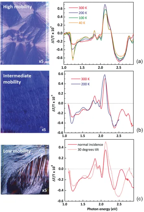
We now turn to a more detailed investi-gation of the origin of the shallow traps in TIPS-P, which cause charge carriers to sense a fully localized environment at low temperature. From the comparison with the other materials we have seen that such pronounced localiza-tion is not a common feature of high-mobility molecular semiconductors. In an attempt to gain insight into why TIPS-P is different, we measured the temperature-dependent CMS spectra of three TIPS-P devices from the same batch of material but with different thin fi lm morphology and device performance: a high-mobility sample (1.4 cm 2 V −1 s −1 ) exhibiting a neat spherulitic microstructure, an inter-mediate-mobility sample (0.8 cm 2 V −1 s −1 ) with a needle-like thin fi lm structure, and a low-mobility sample (0.3 cm 2 V −1 s −1 ) which displays a much thicker and coarser needle microstructure, and overall more randomly oriented crystals (note that these surface mor-phologies were not achieved as part of a con-trolled process but are rather a product of the randomness associated with environmental (glovebox) conditions on the day of fabrication, see Figure 4 ).
Interestingly, in the low-mobility fi lms showing a needle-like microstructure we observed for the fi rst time a charge-induced absorption ≈1.2–1.3 eV that was already some-what sharp at room temperature (Figure 4 ). In the intermediate-mobility sample, the radical cation peak at 1.2–1.3 eV sharpens upon cooling too such that at 200 K it very clearly resembles that of the cation in solu-tion, whilst one could see this in the spheru-litic sample only at very low temperatures. At room temperature the peak at 1.2–1.3 eV is most pronounced in the low-mobility sample; it is somewhat broadened compared to that in the low temperature spectrum in the high
mobility sample, presumably as a result of thermal broad-ening. This suggests that the density of the shallow traps that is responsible for the localization of the carriers at low temperature in our highmobility TIPSP sample has increased signifi -cantly in the needle-like samples and already manifests itself in the nature of charges at room temperature. It is plausible that such poorly connected surface microstructures create bottle-necks to charge carrier transport and are directly responsible for the sharp decrease in FET mobility. But could grain-boundaries
alone, such as microsize gaps between crystals or twin bounda-ries, be the origin of the shallow trap states in TIPS-P observed in CMS? Because CMS measures an average spectrum over all charge carriers in the channel, the low temperature spectrum would imply that all charge carriers would then have to be located in grain boundaries at low temperatures. Furthermore grain boundaries exist in high density in other fi lms such as those we produced with diF-TES-ADT [ 18 ] yet do not lead to tem-perature-dependent CMS in the subgap region.
www.MaterialsViews.com
Figure 4. Device optical images (left) and associated charge modulation spectra (right) of three TIPS-P samples: a) a high-mobility, spherulitic sample ( µ = 1.4 cm 2 V −1 s −1 ), b) an
interme-diate-mobility sample (µ = 0.8 cm 2 V −1 s −1 ), and c) a low-mobility sample ( µ = 0.3 cm 2 V −1 s −1 )
with a coarse needle-like microstructure, given at relevant temperatures. The red, dotted line in the spectrum of sample (c) shows the signal measured with the sample oriented 30° to the normal of the incident light, at 300 K. The differences between the two spectra suggest that there are some interference effects present particularly at higher photon energies.
APER
The differences between the two spectra shown in Figure 4 c measured with the sample oriented 30° to the normal of the incident light show that there are some interference effects pre-sent, which prevent us from interpreting the subtle features in the spectra particularly at higher photon energies. However, in the region ≈1.2 eV these are relatively minor demonstrating that the peak at 1.2 eV observed already at room temperature in the low mobility sample does not stem from interference artefact. In addition, we emphasize that any differences in the spectra observed with temperature, such as the sharpening of the peak ≈1.2 eV with decreasing temperature observed in the other two samples, are unlikely to be caused by interference effects because the changes in the optical thickness of the active device stack that occur with temperature due to thermal contraction/expansion are expected to be negligibly small compared to the large changes in effective optical thickness that are involved when changing the angle of incidence from normal incidence to 30° incidence.
The observed behavior can be consistently explained as fol-lows. In TIPS-P there are clearly specifi c traps states, most likely within the grains that are able to localize the charge carriers onto individual molecules at low temperatures. In contrast in diF-TES-ADT the charge carriers may be confi ned to individual grains at low temperature by potential barriers associated with grain boundaries but are not trapped on the molecular scale. The similarity of the low-temperature and room-temperature CMS spectra implies that charge carriers in diF-TES-ADT remain mobile within the grains even at low temperature. The activation energy of the mobility in diF-TES-ADT can then be considered to refl ect the grain boundary potential. This interpretation is con-sistent with previous studies on these materials. Evidence for the absence of long-lived traps within the grains of spin-casted diF-TES-ADT transistors was previously reported by Marohn and co-workers. [ 19 ] In their time-resolved electric force micros-copy study, the authors also found evidence for intragrain trap states in TIPS-P solution-processed thin fi lms, which supports our hypothesis. At this stage it is necessary to comment on the difference in charge traps observed by the two techniques. The electric force miscrosopc (EFM) experiment observed deep trap states that capture charges over timescales longer than seconds, whereas in CMS we observe shallow trap states in which charge carriers are still able to respond to gate voltage modulations on the time scale of 10 ms. It is possible that the states probed in TIPS-P CMS measurements are precursor states to deep charge traps in which a charge carrier circulates around a defect for some time, before it is fully captured in a deep trap state.
At present we cannot identify the nature of the defect within the grains of TIPS-P that causes the morphology dependent locali-zation of carriers at low temperatures. The defects may well be a chemical impurity that is present in higher density in our needle fi lms than in our spherulitic sample, to levels such that their pres-ence is sensed by charge carriers already at room temperature. Our needle morphology samples were fabricated during a period of increased oxygen concentration in the laboratory glovebox. The low-mobility sample was fabricated fi rst, then the intermediate-mobility sample and fi nally the high-intermediate-mobility sample, as the oxygen content fell down to its normal level. This is consistent with an impurity from oxidation or photochemical degradation rather than from synthesis. Oxygen in combination with light results in oxygen radicals that react with organic semiconductors and it is
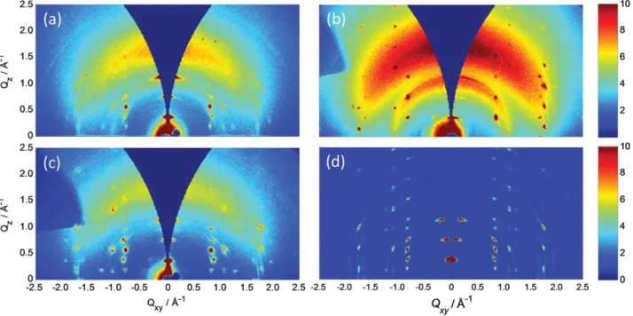
known that TIPS-P is prone to endoperoxide formation [ 20 ] DiF-TES-ADT has been found to be more stable against photooxida-tion than pentacene based materials, which could explain why we see no such trap in the grains of diF-TES-ADT. The mechanism by which oxidation of TIPS-P infl uences crystallization kinetics and fi lm morphology is not understood, but we note that similar observations on the correlation between chemical impurities and fi lm morphology have been made in other systems. Needle-like surface structures formed by impurities segregating to the top of C8-BTBT fi lms during spin coating were reported recently. [ 21 ] We attempted to detect differences in the crystal packing/polymorphs present in the different fi lms using grazing-incidence X-ray fraction (GI-XRD), ( Figure 5 ). The fi lms show broadly similar dif-fraction patterns, which when compared with the model advanced by Anthony et al. [ 22 ] indicate that the a – b plane of the unit cell is parallel to the substrate, i.e., the TIPS-pentacene molecules have their long edge oriented edge-on to the substrate. [ 23 ] However, there are some clear differences in the diffraction patterns of the three fi lms. The intermediate mobility sample with needle-like morphology has diffraction spots missing, which may be attrib-uted to the long-range molecular alignment present in these fi lms, which means that they cannot be considered as isotropic in the plane of the fi lm. There are also more subtle differences in the position of diffractions spots of the high and low mobility samples, which might indicate that the fi lms might comprise subtly dif-ferent polymorphic structure [ 24 ] A detailed microstructural analysis of the different fi lms goes beyond the scope of our spectroscopy focused study. However, from the GI-XRD we cannot exclude the possibility that the different trapping behavior of the TIPS-P fi lms could not be due to a chemical defect, but a structural defect in the bulk or at the active interface. To identify unambiguously the nature of these traps is challenging and will require the application of highly sensitive, analytical techniques. [ 25 ]
3. Conclusion
Our study demonstrates that CMS is a powerful tool to study the correlation between the spectroscopic signature of charge traps and their effect on the temperature dependent charge transport properties as a function of molecular structure. We have observed clear spectroscopic evidence that in certain acene-based polycrystalline fi lms the shallow charge traps within the grains, that localize charges onto single molecules at low temperatures in materials such as TIPS-P and TMTES-P, can be prevented. In systems, such as diF-TES-ADT and β-TMTIPS-P, the spectroscopic properties of charge carriers at low temperatures are very similar to those at room temperature suggesting that the charges remain mobile at low tempera-ture within individual domains/grains. We cannot yet observe clean intrinsic transport properties in FET measurements at low temperature, possibly as a result of charge transport bot-tlenecks associated with grain boundaries or contact resist-ance. To remove these will require further optimization of fi lm/ device processing or application of techniques that probe trans-port on a shorter length scale. However, CMS provides us with a powerful technique for identifying clean molecular systems in which intrinsic transport properties could, in principle, be observed at low temperatures.
FULL P
APER
www.MaterialsViews.com
4. Experimental Section
Top gate, bottom contact thin fi lm transistors with spin-coated organic semiconductor and Cytop fi lms under nitrogen atmosphere were prepared on polyimide-coated glass substrates to help wettability. 10 nm thick gold and 5 nm thick aluminum source drain and gate electrodes, respectively, were used for the charge modulation spectroscopy experiment to reduce interference artefacts and allow semitransparency. The measurements were acquired in accumulation mode with a DC gate voltage of −35 V and an AC modulation bias of ±5 V at 37 Hz without drain voltage ( V D = 0 V).
The Cytop thickness for all samples was 500 ± 30 nm.
Grazing incidence measurements were carried out at room temperature using the Rigaku rotating Cu-anode setup at DTU Energy, monochromatized using Xenocs multilayer mirror to wavelength λ = 1.542 Å (Cu K α). The sample-detector distance was 120 mm,
and the scattered radiation collected using Fuji imaging plates in vacuum, with exposure times of about 180 min. The intensity levels indicate the number of photon counts. The raw data images were numerically interpolated to rectilinear reciprocal space coordinates ( Q xy , Q z). Simulations of the crystalline scattering were done using
SimDiffraction , [ 23 ] based on the crystallographic structure suggested by
Anthony et al. [ 22 ] Preferred 001 orientation with a distribution width of 3°
(fwhm) was assumed, and the overall intensity scaling factor was fi tted.
Supporting Information
Supporting Information is available from the Wiley Online Library or from the author. The data underlying this publication are available at https://www.repository.cam.ac.uk/handle/1810/252545
Acknowledgements
The authors acknowledge material supply and fi nancial support from Merck Chemicals Ltd through an industrial EPSRC CASE studentship. In addition, the work in Mons was supported by the Programme d’Excellence de la Région Wallonne (OPTI2MAT project) and FNRS-FRFC. D.W.B. acknowledges fi nancial support from the Norwegian Research Council.
Received: June 19, 2015 Revised: October 8, 2015 Published online: December 9, 2015
[1] J.-L. Bredas , J. P. Calbert , D. A. da silva Filho , J. Cornil , Proc. Natl. Acad. Sci. USA 2002 , 99 , 5804 .
[2] S. Fratini , D. Mayou , S. Ciuchi , arXiv preprint 1505.02686 . [3] J. E. Anthony , J. Gierschner , C. A. Landis , S. R. Parkin , J. B. Sherman ,
R. C. A. Bakus , Chem. Commun. 2007 , 4746 . [4] A. Troisi , G. Orlandi , Phys. Rev. Lett. 2006 , 96 , 86601 . [5] S. Ciuchi , S. Fratini , D. Mayou , Phys. Rev. B 2012 , 83 , 081202 . [6] S. Coropceanu , J. Cornil , D. A. da Silva Filho , Y. Olivier , R. Silbey ,
J.-L. Brédas , Chem. Rev. 2007 , 107 , 9262.
[7] J. F. Chang , T. Sakanoue , Y. Olivier , T. Uemura , M. B. Dufourg-Madec , S. G. Yeates , J. Cornil , J. Takeya , A. Troisi , H. Sirringhaus , Phys. Rev. Lett. 2011 , 107 , 066601 .
[8] H. Sirringhaus , T. Sakanoue , J. F. Chang , Phys. Status Solidi B 2012 , 249 , 1655 .
[9] V. Podzorov , E. Menard , A. Borissov , V. Kiryukhin , J. A. Rogers , M. E. Gershenson , Phys. Rev. Lett. 2004 , 93 , 86602 .
Figure 5. Grazing incidence X-ray diffraction on the various samples: a) high mobility spherulitic sample, b) intermediate mobility needle-like mor-phology, and c) low mobility coarse needle-like morphology. All the samples exhibit a high crystallinity and are highly oriented out-of-plane. While the samples in (a) and (c) have in-plane isotropy, the sample in (b) has considerable in-plane orientation, as evidenced by the imperfect mirror symmetry with many missing refl ections. The approximate intensity scale is linear and proportional to the number of photons collected. The “nose” seen on the left edge in (b) and (c) is an experimental artifact (shadow from the sample holder). d) Scattering simulation made assuming that the previously reported bulk structure [ 22 ] applies to the thin fi lm, having the crystallites oriented with the a–b plane parallel to the substrate, i.e., (001) orientation. The
simulated pattern bears a strong resemblance to the experimental patterns, but upon closer inspection, it is seen that there are signifi cant differences even in the relative positions of the low index refl ections.
APER
[10] M. E. Gershenson , V. Podzorov , A. F. Morpurgo , Rev. Mod. Sci.
2005 , 78 , 973 .
[11] T. Sakanoue , H. Sirringhaus , Nat. Mater. 2010 , 9 , 736 .
[12] C. Liu , T. Minari , X. Lu , A. Kumatani , K. Takimiya , K. Tsukagoshi , Adv. Mater. 2011 , 23 , 523 .
[13] S. Verlaak , P. Heremans , Phys. Rev. B 2007 , 75 , 115127 .
[14] J. Veres , S. D. Ogier , S. W. Leemingm , D. C. Cupertino , S. M. Khaffaf , Adv. Funct. Mater. 2003 , 13 , 199 .
[15] T. Richards , M. Bird , H. A. Sirringhaus , J. Chem. Phys. 2008 , 28 , 234905 . [16] N. G. Martinelli , M. Savini , L. Muccioli , Y. Olivier , F. Castet , C. Zannoni , D. Beljonne , J. Cornil , Adv. Funct. Mater. 2009 , 19 , 3254 . [17] S. Subramanian , K. P. Sung , S. R. Parkin , V. Podzorov , T. N. Jackson ,
J. E. Anthony , J. Am. Chem. Soc. 2008 , 130 , 2706 .
[18] S. K. Park , D. A. Mourey , S. Subramanian , J. E. Anthony , T. Jackson , App. Phys. Lett. 2008 , 93 , 043301 .
[19] M. J. Jaquith , J. E. Anthony , J. A. Marohn , J. Mater. Chem. 2009 , 19 , 6116 .
[20] I. Kaur , W. Jia , R. P. Kopreski , S. Selvarasah , M. R. Dokmeci , C. Pramanik , N. E. McGruer , G. P. Miller , J. Am. Chem. Soc. 2008 , 130 , 16274 .
[21] Y. Li , C. Liu , M. V. Lee , Y. Xu , X. Wang , Y. Shi , K. Tsukagoshi , J. Mater. Chem. C 2013 , 1 , 1352 .
[22] J. E. Anthony , J. S. Brooks , D. L. Eaton , S. R. Parkin , J. Am. Chem. Soc. 2001 , 123 , 9482 .
[23] D. W. Breiby , O. Bunk , J. W. Andreasen , H. T. Lemke , M. M. Nielsen , J. Appl. Crystallogr. 2008 , 41 , 262 .
[24] R. Kamiya , T. Hosokai , T. Watanabe , T. Koganezawa , M. Kikuchi , N. Yoshimoto , Mol. Cryst. Liq. Cryst. 2012 , 568 , 134 .
[25] F. De Angelis , M. Gaspari , A. Procopio , G. Cuda , E. Di Fabrizio , Chem. Phys. Lett. 2009 , 468 , 193 .