HAL Id: hal-01821024
https://hal.archives-ouvertes.fr/hal-01821024
Submitted on 22 Jun 2018HAL is a multi-disciplinary open access archive for the deposit and dissemination of sci-entific research documents, whether they are pub-lished or not. The documents may come from teaching and research institutions in France or abroad, or from public or private research centers.
L’archive ouverte pluridisciplinaire HAL, est destinée au dépôt et à la diffusion de documents scientifiques de niveau recherche, publiés ou non, émanant des établissements d’enseignement et de recherche français ou étrangers, des laboratoires publics ou privés.
In situ Bragg coherent X-ray diffraction during tensile
testing of an individual Au nanowire
J. Shin, T. Cornelius, S. Labat, F. Lauraux, M.-I. Richard, G. Richter,
Nicholas Blanchard, D. Gianola, O. Thomas
To cite this version:
J. Shin, T. Cornelius, S. Labat, F. Lauraux, M.-I. Richard, et al.. In situ Bragg coherent X-ray diffraction during tensile testing of an individual Au nanowire. Journal of Applied Crystallography, International Union of Crystallography, 2018, 51 (3), pp.781-788. �10.1107/S1600576718004910�. �hal-01821024�
In situ Bragg coherent X-ray diffraction during tensile testing of an
individual Au nanowire
J. Shin1,2,3, T.W. Cornelius1, S. Labat1, F. Lauraux1, M.-I. Richard1,4, G. Richter5, N. P.
Blanchard6, D.S. Gianola3, O. Thomas1
1
Aix Marseille Univ, Université de Toulon, CNRS, IM2NP, Marseille, France
2
University of Pennsylvania, Philadelphia, PA, USA
3
University of California – Santa Barbara, Santa Barbara, CA, USA
4
European Synchrotron Radiation Facility (ESRF), 6 rue Jules Horowitz, BP 220, F-38043
Grenoble Cedex, France
5
Max Planck Institute for Intelligent Systems, Heisenbergstrasse 3, 70569 Stuttgart, Germany
6
University of Lyon, Université Claude Bernard Lyon 1, CNRS, Institut Lumière Matière,
F-69622, VILLEURBANNE, France
Abstract
We report on systematic single defect free <110> Au nanowires grown by physical vapor deposition in situ tensile tests while simultaneously recording 3D Bragg peaks using coherent X-rays. The trajectory of 3D Bragg peaks in reciprocal space during tensile testing allowed for measurements of the evolution of strains and rotations of the nanowire, thus sensitively uncovering the full deformation geometry of the nanowire. The transition from elastic to plastic deformation is accompanied by rotations of the nanowire as quantified by analysis of the motion of Bragg peaks, showing the importance of boundary conditions in interpreting nanoscale mechanical deformations.
Keywords: Bragg coherent X-ray diffraction, in situ tensile test, nanowire, small scale deformation
1. Introduction
Novel electronic, nano/micromechanical, and energy storage devices incorporate nanoscale features that experience mechanical stresses, thereby highlighting the need for structural integrity of the building block materials and necessitating nanomechanical testing approaches with requisite spatial resolution and crystallographically-resolved information (Kraft et al., 2010; Zhu & Li, 2010). Beyond scaling effects that bring the importance of interfaces and surfaces into sharp focus, new deformation mechanisms emerge in nanostructured materials that must be elucidated. For instance, the lack of pre-existing mobile plasticity carriers such as dislocations gives rise to ultra-high strength approaching the theoretical limit (Richter et al., 2009; Greer & Nix, 2006; Bei et al., 2008), and consequently, large elastic strains leading to nonlinear (post-Hookean) elastic deformation can be experienced (Chen et al., 2012) which now have to consider significance of surface layer contribution to its bulk response including diffusional process (Chen et al., 2015; Zhong et
al., 2016). Whereas the onset of plasticity in bulk ductile materials is governed by activation
of existing dislocation sources, this gives way to the importance of nucleation of new dislocations in the otherwise pristine crystal. A common denominator in the elastic and plastic properties of emerging nanomaterials is the importance of the near surface and interface response, yet a limited experimental toolkit precludes a complete understanding of these phenomena. In situ imaging techniques allowing for the direct observation of defect-level dynamics have shown tremendous advances (Lu & Lou, 2011; Uchic et al., 2004; Iqbal et al., 2012; Zhu & Espinosa, 2005; Zhu et al., 2006; Kiener & Minor, 2011; Seo et al., 2011), although quantification of the full deformation trajectory using electron microscopes is challenging.
The newest generation of X-ray sources, particularly coherent X-ray sources ameliorate many of these issues and paves the way for in situ nanomechanical testing with real-time diffraction, fully in 3D (Robinson & Harder, 2009). By far, the best spatial
resolution is obtained with Bragg coherent diffraction imaging (BCDI), which is a lensless imaging technique, with a typical resolution of 8-10 nm (Labat et al., 2015). In addition, with the aid of phase retrieval algorithm (Fienup, 1982; Minkevich et al., 2008), it allows for spatially characterizing individual defects and dislocation networks in crystals (Labat et al., 2015; Kirchlechner et al., 2011; Hofmann et al., 2017; Clark et al., 2015) as well as the full elastic strain tensor deduced from crystallographically resolved displacement fields (Haag et
al., 2013; Newton et al., 2010). X-ray experiments offering the unique advantages of being
nondestructive, volume probing, and exquisitely sensitive to small strains makes BCDI an ideal tool for such nanomechanical testing, yet in situ experiments using these new modalities are still nascent (Miao et al., 2015; Leclere et al., 2015; Ren et al., 2014; Maaß et al., 2009; Dupraz et al., 2017). In particular, the application of these methods to much less complex stress states – and thereby more easily interpretable phenomena – such as in situ tensile testing of quasi-1D nanoscaled specimens would enable substantial progress. Recent developments of in-situ synchrotron X-ray diffraction studies of the mechanical behavior of materials at small scales were reviewed in ref. (Cornelius & Thomas, 2018).
In the present work, we show for the first time the successful in situ combination of Bragg coherent X-ray diffraction (BCD) during tensile testing of a single Au nanowire using a microelectromechanical system (MEMS) based tensile stage. This uniaxial testing approach applied to a single nanowire greatly simplifies the stress state and enables a more facile interpretation of deformation events. This in situ technique not only allows for the tracking of the evolution of lattice strain in the nanowire during mechanical testing but also rotational changes of the nanowire (such as twisting and bending) that arise during the tensile test with unprecedented accuracy, enabling the inference of the events leading to plastic initiation as well as plastic flow in small-scale FCC materials.
Nominally defect-free <110> oriented single-crystalline gold nanowires were grown by physical vapor deposition on tungsten substrates under ultra-high vacuum conditions with molecular beam epitaxy method, similar to the conditions reported in (Richter et al., 2009). These defect-free nanowires were coated with a 2 nm thick Al2O3 layer by atomic layer deposition. Using a nano-manipulator in a scanning electron microscope, the as-grown nanowires were harvested, aligned, and transferred to a thermally actuated MEMS-based tensile stage (Chen et al., 2014; Murphy et al., 2013) where they were affixed to the stage grips with Pt-containing material by electron beam induced deposition (EBID) as shown in Fig. 1(a). The tensile stage is operated by Joule heating of the thermal actuator beams, while the applied load is determined by displacement of the load cell with a pre-calibrated stiffness (Chen, 2014).
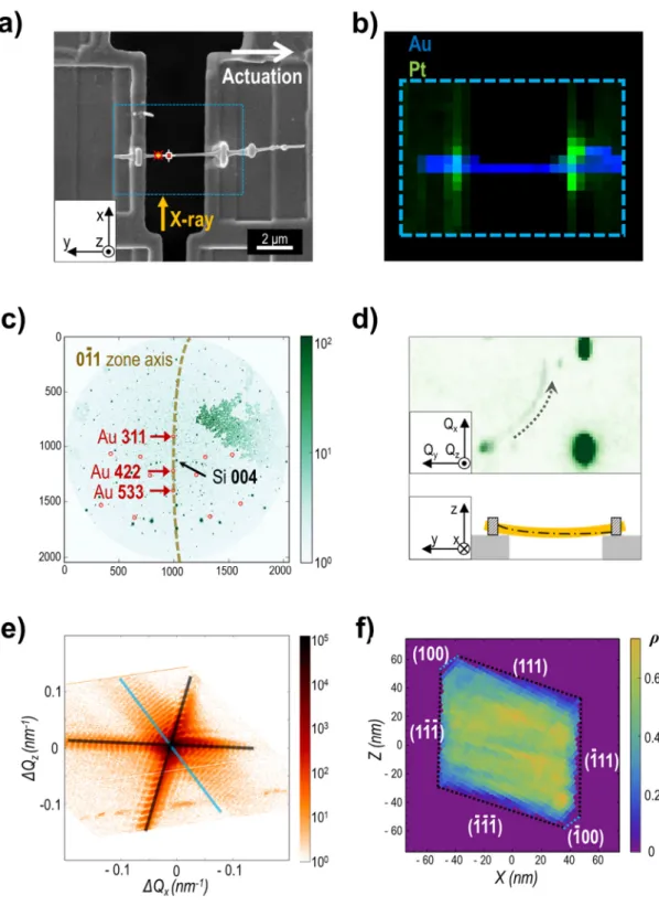
In addition to the known growth direction, the precise nanowire orientation on the tensile stage was determined by Laue microdiffraction at the BM32 beamline at the European Synchrotron Radiation Facility (ESRF) to determine the appropriate Bragg condition for BCDI. The incident polychromatic beam was focused down to 500 nm × 500 nm on the sample surface by a pair of Kirkpatrick-Baez (KB) mirrors and the diffracted X-rays were recorded by a MarCCD as shown in Supplementary (Fig. S1. (a)). The fluorescence yield was monitored simultaneous with diffraction data using a Röntec XFlash 1001 energy-resolved point detector to identify the nanowire and to properly position it with the incident beam. The nanowire was located by scanning the sample in steps of 500 nm (corresponding to the beam size) through the focused polychromatic X-ray beam and recording both the Au Lα1 and the Pt Lα1 fluorescence. The corresponding map superimposing the two fluorescence yields is displayed in Fig. 1(b), clearly visualizing the Au nanowire and the Pt glue with sufficient spatial resolution for subsequent beam placement. The recorded Laue diffraction patterns were analyzed using the LaueTools software (Robach & Micha, 2015) to determine the wire orientation with respect to the laboratory coordinates. We set the laboratory axes x as
perpendicular to the tensile direction (projected direction of the incoming X-ray to the substrate), y as the tensile direction, and z normal to the substrate as depicted in Fig. 1(a).
Throughout the subsequent in situ tensile tests simultaneous with BCD, the Au 311 Bragg peak, with corresponding planes parallel to the wire axis, was tracked to determine the strain and rotation of the nanowire. The in situ tensile tests were conducted at the ID01 beamline at ESRF and started by adjusting the specimen to diffraction conditions for the Au 311 Bragg peak based on the information obtained by Laue microdiffraction. Here, an 8 keV incident X-ray beam was focused down to 150 nm (V) × 400 nm (H) using a Fresnel zone plate (FZP) with a diameter of 300 µm and an outer zone width of 70 nm. The coherent part of the incident X-ray beam was selected by closing slits installed in front of the FZP to 200 µm (V) × 60 µm (H), thus matching the lateral coherence lengths of the beamline. The coherent beam-exposed area during the tensile tests is marked in Fig. 1(a) and the diffracted X-rays were recorded by a 2D MAXIPIX detector with a pixel size of 55 µm × 55 µm installed 400 mm downstream of the sample position. The three-dimensional BCD pattern was recorded by rocking the sample by +/- 1° (corresponding to ∆Q = +/- 0.9 nm-1). Two different positions along the nanowire, 500 nm apart from each other marked with P1 and P2 in Fig. 1(a), were measured to understand the comprehensive deformation behavior. The MEMS chip was first wire bonded to a custom designed printed circuit board (PCB) to connect a source measure unit (Keithley 6487) to actuate the tensile stage with applied voltage (Fig. S1). The PCB was then mounted on the ID01 goniometer. The actuation displacement was calibrated beforehand without the specimen. The nanowire tensile experiments proceeded as follows: Tests 1-4 consisted of progressively increasing load-unload experiments. Test 1 and Test 3 were measured at position 1 (P1), and Test 2 and Test 4 were measured at position 2 (P2). Tests 1 to 3 were simple load-unload cycles and Test 4 included a partial unload. The evolution of the peak obtained from 3D BCD patterns was measured at every increment of displacement of the MEMS actuator. For the lattice strain determination, the movement of the 311 peak in
reciprocal space was used to calculate the compressive strain. This Poisson strain was subsequently converted to a [0 1 1] tensile strain by using the elastic constants of bulk Au (Hiki & Granato, 1966). In addition to lattice strains, the deconvoluted angular evolution of the 311 peak in reciprocal space with respect to the first scan was also measured to analyze the rotational movement of the nanowire throughout the test.
3. Results and Discussion
We first demonstrate the use of Laue microdiffraction to map the full crystallography and orientation of the as-prepared nanowire. A representative Laue microdiffraction pattern is shown in Fig. 1(c) with the vertical and the horizontal axes representing the projection of angles about y (Bragg angle axis) and of angles about x (incident beam direction), respectively. The Laue spots originating from the Au nanowire are marked with red circles which were selected from the background Si peaks coming from the MEMS device. The dashed line in Fig. 1(c) connecting the Au peaks belonging to the [0 1 1] zone axis confirms the nanowire growth direction. The rotational orientation of the nanowire was determined from the angle between the Si 004 and the Au 111 Laue spots revealing that the nanowire was affixed with the top facing {111} facet pitched by 13 ° with respect to the normal surface of the tensile stage. Mapping of the full nanowire orientation as positioned for mechanical testing allowed for facile navigation of reciprocal space at ID01.
In addition to the orientation, rotations of the crystal lattice due to bending and torsion along the nanowire prior to external loading was inferred from the movement of the Laue spots on the detector while the X-ray beam scanned along the nanowire. The integrated Laue pattern in the vicinity of the Au 311 Laue spot (Fig. 1(d)) demonstrates that the 4 µm of suspended portion of the nanowire was twisted about the y-axis (tensile axis) by 1.3 ° and bent about the x-axis (incoming beam direction) by 1.0 ° as illustrated in the inset. We ascribe
this pre-deformation of the nanowire to the manipulation process; the characterization of this state is crucial for accurately interpreting the deformation trajectories during subsequent in
situ tensile testing.
The Qx-Qz slice of the 3D Bragg peak of the as-manipulated nanowire is presented in Fig. 1(e), which contains streaks and corresponding size fringes reflecting the shape of the nanowire. The real space cross sectional view of the nanowire was reconstructed from the slice of the 3D Bragg peak (Fig. 1(f)) unveiling that the nanowire is composed of four large {111} facets indicated by black dotted lines and two smaller {100} side facets delineated by blue dotted lines which can be matched with the fringe pattern in Fig 1(e). The mean distance between the two sets of {111} facets are approximately 90 nm and 100 nm, and the {100} facets are 140 nm apart from 4 nm pixel resolution.
The [0 1 1] tensile lattice strains calculated from the 311 compressive strain for Tests 1-4 are shown in Fig. 2(a) with overlaid actuator input displacements. The lattice strain responds proportionally to the input displacement. For applied displacements below 100 nm (Test 1), the lattice strain is negligible and can be explained by a pre-buckled nanowire as corroborated by the prior Laue microdiffraction analysis. For small applied deformations, the lattice may rotate but the lattice strain increases only after the wire is pulled taut. While Test 2 showed full recovery of the lattice strain, residual strain was detected after Test 3. This can be explained with a resistance upon returning to the buckled state, which is further discussed later, by an extra coating that was incurred during the experiment.
In Fig. 2(b), the evolution of the Bragg peak during the tensile test is shown for four representative tensile strain states selected from Test 3 and Test 4 by displaying the projection of the Bragg peak along the reciprocal space vector Qz. Although the two tests were measured 500 nm apart, the shape itself is worth comparing to understand the deformation behavior of the nanowire. Similar to Fig. 1(d), the initial elongation of the Bragg reflection along Qx
originated from the nanowire torsion whereas the elongation along Qy was caused by the
nanowire bending. The Au 311 peak shape at 0% strain further depicts a non-homogeneous bending of the nanowire. From Laue microdiffraction, a bending close to 0.1 ° is expected for 400 nm illuminated area along the wire. However, the measured bending is about 0.3 ° (full width at half maximum fit) which suggests higher bending angle near the left side grip. Nevertheless, the torsion in this range agrees with the Laue microdiffraction measurement. The peak profile at higher strain states (1.8% in Fig. 2(b)) shows the torsion remaining constant upon application of tensile strain, however, the elongation along Qy diminishes with
increasing tensile strain indicating a taut wire.
Combining the in situ Bragg coherent diffraction data with global strain measurements determined by digital image correlation (DIC) allows a comparison of the accuracy and importance of the lattice strain. We define the DIC strain as that measured from the displacement of the grip opening (grip displacement) from the optical microscope image. We now concentrate on Test 3 and Test 4 where larger displacements were applied. Fig. 2(c) shows a correspondence between both strain measures although the DIC strain values are systematically larger than the lattice strain. This discrepancy is attributed to the compliance of the Pt EBID that had been used to fix the nanowire, demonstrating the significance of obtaining lattice strain from diffraction data.
The load applied to the system can be calculated from DIC measured displacement and the known stiffness of the load cell. The maximum force applied to the nanowire was calculated to be 24.6 µN. Using the cross-sectional area obtained by the 2D reconstruction (Fig. 2(f)) of the coherent Au 311 Bragg peak, the highest strength is calculated to be of the order of 2.9 GPa. This value is much higher than an axial stress of 1.68 GPa obtained by using the Young’s modulus of bulk Au along [0 1 1] and the lattice strain deduced from BCD. This
discrepancy is explained later by the load bearing of a contamination layer formed around the nanowire during the experiment.
The Bragg peak evolution is capable of precisely determining the lattice rotations during
in situ tests. Fig. 3(a) shows the overall movement of the Au 311 peak and its displacement in
reciprocal space (determined by extracting the center of mass of the Bragg peak) during the tensile test. The peak mainly moves along the Qx-Qy plane, indicating that the nanowire
primarily rotated about the z axis. This feature is more prominent in Test 3 and Test 4 with higher applied displacement.
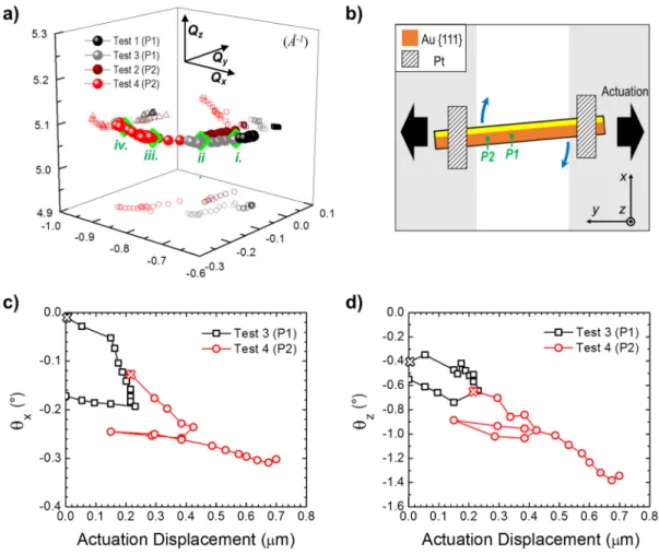
We further analyze this rotational motion by deconvoluting the spatial movement of the peak. The Au 311 Bragg peak shifts in reciprocal space upon tensile actuation, where the length of the diffraction vector determines the lattice strain whereas the rotational movement of the vector characterizes the rotation of the crystal plane. The relative rotational movements of the peak in 3D reciprocal space were resolved along the three orthogonal directions θx, θy, and θz which have rotational axes of Qx, Qy, and Qz, respectively.
Lattice rotations are unexpected during ideal tensile tests in the absence of lateral constraint and other non-ideal boundary and initial conditions. However, the tested nanowire had an initial misalignment in θz by about 2.5 ° as seen in Fig. 1(a). This configuration is illustrated in Fig. 3(b) with the plan view projection of an inclined (311) plane. Moreover, bending and torsion was observed in both Laue microdiffraction and BCD which can introduce lattice rotations during the tensile test. As the tensile test proceeds, the misaligned nanowire (lattice planes) rotates about the z axis (θz) in real space to align with the tensile axis, corresponding to a rotation of the diffraction peak in reciprocal space about Qz and at the
same time, the nanowire straightens which is depicted by θx. Since the torsion nominally remains constant during the experiment θy remainedclose to zero.
Fig. 3(c) and (d) show θx and θz, respectively, as a function of applied displacement in Test 3 and Test 4. As demonstrated in Fig. 3(a), whereas the relative angular movement in θz
(Qx-Qy plane) is predominant, there are still finite changes in θx due to the initial bent
configuration of the nanowire. In both measured positions, the loading and unloading curves do not overlap each other. A lower slope in unloading suggests the nanowire experiences resistance upon returning to its initial state, and can be related to the residual strains observed in Fig. 2(a). In Fig. 3(c), the difference in loading slope between P1 and P2 suggests inhomogeneous bending along the nanowire: more bent down towards the center of the nanowire (P1) than near the grip (P2). The evolution of θz indicates that the (311) plane rotated to compensate the initial misalignment. It generally decreases upon loading and increases during unloading. In addition, the loading slopes are less dependent on the measured position than for θx. Another important aspect is the fact that the angular motion reverses its course at the end of Test 4 for both θx and θz. This opposite turn implies the wire relaxed toward its initial misaligned configuration caused by yielding with a corresponding stress of 1.63 GPa.
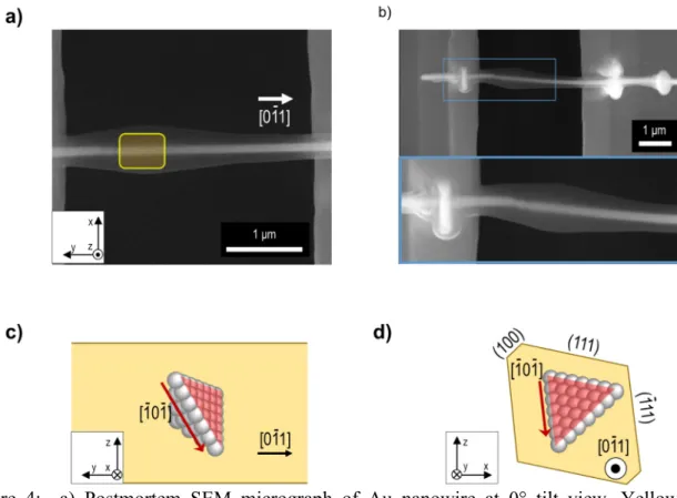
Permanent deformation of the nanowire was confirmed by post-mortem SEM imaging as demonstrated in Figs. 4(a) and (b). The yellow rectangle in Fig. 4(a) indicates the size of the footprint of the incident coherent X-ray beam on the sample surface. In this plan view, the plastically deformed nanowire appears rather straight. However, the plastically deformed area is more noticeable in the 24.5 ° angled view in Fig. 4(b) which shows that the wire has lengthened because of plastic deformation and subsequently buckles upon unloading. The angled view indicates that slip proceeded downwards along the negative z direction. Based on the deformation geometry, the activated slip plane can be inferred as ( 1 1 1) with [0 1 1] being the tensile axis. Evidence of extended deformation twin was not detected in BCD within the beam illuminated area which suggests the deformation morphology includes multiple of nanotwins (Roos et al., 2014; Lee et al., 2014; Sedlmayr et al., 2012) presumably having possible partial slips directions of [ 1 1 2 ] and [ 2 1 1 ].
Previously, the yield stress showed notable discrepancy between stress values calculated from DIC measured force and lattice strain to stress conversion methods. By comparing between Fig. 1(a) and Fig. 4(a), excessive coating was formed during the experiment. The layer likely originated from X-ray beam induced deposition (XBID) of hydrocarbons (Haag et
al., 2013) from the atmosphere or diffusion of organometallic material from the Pt-EBID
grips during the multiple-day experiment. This extra coating normally does not act as significant load bearing when the thickness is small. However as confirmed by SEM, the volume fraction exceeds more than 90% of the whole tested volume. This significant volume fraction of coating deposited during the test makes difficult to obtain yield strength solely from the DIC measurements.
Instead, we utilize the SEM measured coating thickness and the information from the tensile lattice strain and cross-sectional area of the nanowire from the reconstruction to evaluate the XBID coating property with the assumption of elastic loading of an iso-strained composite. The estimated elastic modulus of the coating yielded 4.3 GPa which is about 1 order of magnitude smaller than that of carbon deposition with a 12 kV electron beam (Ding
et al., 2005). This suggests either the XBID forms weaker bonding strength than the e-beam
or the coating was elasto-plastically deforming during the test. With the elastic modulus of the XBID coating we could recalculate the yield strength of the nanowire without using the bulk Au elastic property. By subtracting the load bearing of the coating, the discrepancy between the yield strength drops to 5% with the estimated nanowire strength of 1.61 GPa.
On the other hand, elasto-plastically deforming the XBID coating can augment the explanation of the hysteresis observed in the strain and rotation during the actuation cycles. The consequent relaxation of the XBID coating can undergo compressive stress upon unloading, which can manifest as the observed hysteresis. Both residual lattice strain and uneven behavior in angular movement were observed from the load-unload cycles. If the coating undergoes relaxation after a loading step, then this considerable external layer
experiences compressive stress to reconfigure its structure upon unloading which may not necessarily have to be the shape it had before. This phenomena can hold the nanowire in tension for a while, and also inhibit the wire from returning to its initial bent configuration.
The key component of the stress evaluation was the reconstructed shape of the nanowire. The diameter measured from SEM plan view is 109 nm which only contains 2D information. The area calculated from circular cross-sectional assumption is 7% larger than the polygon area calculated from the reconstructed shape. This discrepancy is not large in the current case but depending on the chosen plan view the error could have varied from 30% smaller to 70% larger for the relevant calculations. From this reason, in situ nanowire tests in electron microscopes may suffer from obtaining accurate strength of the tested volume, which also highlights a strength of BCD in situ tests.
4. Conclusion
This work presents, to our knowledge, the first successful combination of in situ tensile testing of a single nanowire with BCD. This in situ technique provides the full trajectory of deformation of nanowire – strain, bending, and torsion which are often concealed in other testing methods – during mechanical loading. These additional deformations superpose with the tensile strain are of particular importance for the studying fundamental deformation mechanism associated with defect nucleation and the simulation of the experimental findings (Tian et al., 2014; Nöhring et al., 2016). Moreover, this work paves the way to in situ BCDI that would enable the measurement of full 3D strain fields inside the loaded nanostructure with unprecedented accuracy as well as imaging defects, thus providing access to a deeper understanding of stress and defect nucleation.
The authors gratefully acknowledge support of the A*MIDEX grant (ANR-11-IDEX-0001-02) funded by the French Government « Investissements d’Avenir » program and the European Synchrotron Radiation Facility (ESRF) for the allocated experiment at the BM32 and the ID01 beamlines. The research reported here was supported by the NSF MRSEC Program through DMR 1720256 (IRG-1). The authors would also like to thank the Plateforme Nanofils et Nanotubes Lyonnaise for access to the SEM and Imina nano-manipulators.
References
Bei, H., Shim, S., Pharr, G. M. & George, E. P. (2008). Acta Mater. 56, 4762–4770. Chen, L. Y. (2014). Publicly Access. Penn Diss. Paper 1049,.
Chen, L. Y., He, M.-R., Shin, J., Richter, G. & Gianola, D. S. (2015). Nat. Mater. 14, 707– 713.
Chen, L. Y., Richter, G., Sullivan, J. P. & Gianola, D. S. (2012). Phys. Rev. Lett. 109, 1–5. Chen, L. Y., Terrab, S., Murphy, K. F., Sullivan, J. P., Cheng, X. & Gianola, D. S. (2014).
Rev. Sci. Instrum. 85, 13901.
Clark, J. N., Ihli, J., Schenk, A. S., Kim, Y., Kulak, A. N., Campbell, M., Nisbit, G., Meldrum, F. C. & Robinson, I. K. (2015). Nat. Mater. 14, 780–785.
Cornelius, T. W. & Thomas, O. (2018). Prog. Mater. Sci. 94, 384–434.
Ding, W., Dikin, D. A., Chen, X., Piner, R. D., Ruoff, R. S., Zussman, E., Wang, X. & Li, X. (2005). J. Appl. Phys. 98, 14905.
Dupraz, M., Beutier, G., Cornelius, T. W., Parry, G., Ren, Z., Labat, S., Richard, M.-I., Chahine, G. A., Kovalenko, O., De Boissieu, M., Rabkin, E., Verdier, M. & Thomas, O. (2017). Nano Lett. 17, 6696–6701.
Fienup, J. R. (1982). Appl. Opt. 21, 2758.
Greer, J. R. & Nix, W. D. (2006). Phys. Rev. B. 73, 245410.
Haag, S. T., Richard, M., Welzel, U., Favre-nicolin, V., Balmes, O., Richter, G., Mittemeijer, E. J. & Thomas, O. (2013). Nano Lett. 13, 1883–1889.
Hiki, Y. & Granato, A. V. (1966). Phys. Rev. 144, 411–419.
Hofmann, F., Tarleton, E., Harder, R. J., Phillips, N. W., Ma, P.-W., Clark, J. N., Robinson, I. K., Abbey, B., Liu, W. & Beck, C. E. (2017). Sci. Rep. 7, 45993.
Iqbal, F., Ast, J., Göken, M. & Durst, K. (2012). Acta Mater. 60, 1193–1200. Kiener, D. & Minor, A. M. (2011). Nano Lett. 11, 3816–3820.
Ulrich, O., Thomas, O., Dehm, G. & Keckes, J. (2011). Philos. Mag. 91, 1256–1264. Kraft, O., Gruber, P. A., Mönig, R. & Weygand, D. (2010). Annu. Rev. Mater. Res. 40, 293–
317.
Labat, S., Richard, M. I., Dupraz, M., Gailhanou, M., Beutier, G., Verdier, M., Mastropietro, F., Cornelius, T. W., Schülli, T. U., Eymery, J. & Thomas, O. (2015). ACS Nano. 9, 9210–9216.
Leclere, C., Cornelius, T. W., Ren, Z., Davydok, A., Micha, J.-S., Robach, O., Richter, G., Belliard, L. & Thomas, O. (2015). J. Appl. Crystallogr. 48, 291–296.
Lee, S., Im, J., Yoo, Y., Bitzek, E., Kiener, D., Richter, G., Kim, B. & Oh, S. H. (2014). Nat.
Commun. 5, 1–10.
Lu, Y. & Lou, J. (2011). Jom. 63, 35–42.
Maaß, R., Van Petegem, S., Borca, C. N. & Van Swygenhoven, H. (2009). Mater. Sci. Eng. A.
524, 40–45.
Miao, J., Ishikawa, T., Robinson, I. K. & Murnane, M. M. (2015). Science. 348, 530–535. Minkevich, A. A., Baumbach, T., Gailhanou, M. & Thomas, O. (2008). Phys. Rev. B. 78,
174110.
Murphy, K. F., Chen, L. Y. & Gianola, D. S. (2013). Nanotechnology. 24, 235704.
Newton, M. C., Leake, S. J., Harder, R. & Robinson, I. K. (2010). Nat. Mater. 9, 120–124. Nöhring, W. G., Möller, J. J., Xie, Z. & Bitzek, E. (2016). Extrem. Mech. Lett. 8, 140–150. Ren, Z., Mastropietro, F., Davydok, A., Langlais, S., Richard, M. I., Furter, J. J., Thomas, O.,
Dupraz, M., Verdier, M., Beutier, G., Boesecke, P. & Cornelius, T. W. (2014). J.
Synchrotron Radiat. 21, 1128–1133.
Richter, G., Hillerich, K., Gianola, D. S., Mönig, R., Kraft, O. & Volkert, C. A. (2009). Nano
Lett. 9, 3048–3052.
Robach, O. & Micha, J.-S. (2015). LaueTools: Open source python packages for X-ray MicroLaue Diffraction analysis.
Robinson, I. & Harder, R. (2009). Nat. Mater. 8, 291–298.
Roos, B., Kapelle, B., Richter, G. & Volkert, C. A. (2014). Appl. Phys. Lett. 105, 201908. Sedlmayr, A., Bitzek, E., Gianola, D. S., Richter, G., Mönig, R. & Kraft, O. (2012). Acta
Mater. 60, 3985–3993.
Seo, J.-H., Yoo, Y., Park, N.-Y., Yoon, S.-W., Lee, H., Han, S., Lee, S.-W., Seong, T.-Y., Lee, S.-C., Lee, K.-B., Cha, P.-R., Park, H. S., Kim, B. & Ahn, J.-P. (2011). Nano Lett.
11, 3499–3502.
Tian, X., Cui, J., Zhang, C., Ma, Z., Wan, R. & Zhang, Q. (2014). Comput. Mater. Sci. 83, 250–254.
Uchic, M. D., Dimiduk, D. M., Florando, J. N. & Nix, W. D. (2004). Science. 305, 986–989. Zhong, L., Sansoz, F., He, Y., Wang, C., Zhang, Z. & Mao, S. X. (2016). Nat. Mater. 1, 1–8. Zhu, T. & Li, J. (2010). Prog. Mater. Sci. 55, 710–757.
Zhu, Y., Corigliano, A. & Espinosa, H. D. (2006). J. Micromechanics Microengineering. 16, 242–253.
Fig. 1: a) SEM micrograph of the as transferred Au nanowire. The markers on the nanowire indicates the two positions (P1 and P2 from the right) where BCD was recorded during the in situ tensile test. b) The Au La1 and Pt La1 fluorescence map of the nanowire c) Laue
microdiffraction pattern of Au nanowire shown in (a). d) Integrated Laue microdiffraction pattern of the Au {311} Laue spot recorded along the Au nanowire shown in (a). The inset illustrates the configuration of the nanowire mounted on MEMS based tensile stage. e) BCD pattern and f) the two-dimensional reconstructed electron density (ρe) map of the
Figure 2. a) [0 1 1] tensile strain response overlaid with the applied actuator displacement during the tests. b) Evolution of the shape from Qz sum of 311 Bragg peak at 0%, 0.5%, 1%
and 1.8% tensile strain. c) Comparison of strain measured with DIC and the lattice strain from Bragg peak analysis d) Load-displacement curve
Figure 3: a) The movement of Au 311 Bragg peak in 3D reciprocal space and their projections along the reciprocal space coordinates. The marked green diamonds are the 4 peaks in Fig. 2b). b) Schematic plan view drawing of tested nanowire and possible rotation during the tensile tests. c) Deconvoluted rotational movement of Au 311 peak of Test 3 (P1) and Test 4 (P2) represented in relative angles about x and d) about z axis. Cross mark represents the first data point of each tests.
Figure 4: a) Postmortem SEM micrograph of Au nanowire at 0° tilt view. Yellow box indicates the beam exposed area. b) Angled view of the tested Au nanowire at 24.5 ° tilt c) Schematic drawing of possible slip system with the side view and d) wire axis view. Possible activated slip plane ( 1 1 1) is highlighted.
![Figure 2. a) [0 1 1] tensile strain response overlaid with the applied actuator displacement during the tests](https://thumb-eu.123doks.com/thumbv2/123doknet/14621287.733738/19.892.114.763.112.604/figure-tensile-strain-response-overlaid-applied-actuator-displacement.webp)