HAL Id: hal-01779825
https://hal.archives-ouvertes.fr/hal-01779825
Submitted on 27 Apr 2018
HAL is a multi-disciplinary open access
archive for the deposit and dissemination of
sci-entific research documents, whether they are
pub-lished or not. The documents may come from
teaching and research institutions in France or
abroad, or from public or private research centers.
L’archive ouverte pluridisciplinaire HAL, est
destinée au dépôt et à la diffusion de documents
scientifiques de niveau recherche, publiés ou non,
émanant des établissements d’enseignement et de
recherche français ou étrangers, des laboratoires
publics ou privés.
MOSFET
K Frifita, Nk M’Sirdi, A Baghaz, M Naamane, M Boussak
To cite this version:
K Frifita, Nk M’Sirdi, A Baghaz, M Naamane, M Boussak. Electro-thermal Model of a Silicon
Carbide Power MOSFET. International Conference on Electronic Engineering and Renewable Energy
(ICEERE’2018), Apr 2018, Oujda, Morocco. �hal-01779825�
Electro-thermal Model of a Silicon Carbide Power
MOSFET
K. Frifita . K. M’Sirdi, E. Baghaz, A. Naamane, and M. Boussak
Aix Marseille Univ, Universite de Toulon, CNRS, LIS, Marseille, France SASV group of LIS UMR CNRS 7020, e-mail: nacer.msirdi@univ-amu.fr
Abstract. This paper proposes an electro thermal model for power
silicon carbide (SiC) MOSFET based on the EKV MOSFET structure. The thermal dissipation is modeled as an RC Network. The model is developed for the SiC MOSFET C2M0025120D CREE (1200V, 90A) and integrated in the Psim, Saber and Pspice simulation software libraries for prototyping. The simulation curves are compared with the manufacturers’ data-sheet.
Keywords: SiC MOSFET, Electro-thermal Model, Psim, Saber, Pspice Model
1 Introduction
The use of a silicon carbide (SiC) for industrial manufacturing power compo-nents such as the MOSFET makes it possible to have high performance which satisfy advanced application problems (time response, environmental stresses, heating, power loss reduced). These constraints affect the electrical behavior of the electronic components by the coupling between the electrical and the thermal behaviors. In high power applications, Silicon (Si) circuits are more and more replaced by SiC MOSFET devices [1]. A first serie of such devices has been proposed by CREE, like the SiC MOSFET C2M0025120D (1200V, 90A) [2]. Simulations are very important in electric systems design. Therefore a good suitable simulation models is required in order to show the faisability of the complex systems [3, 4].
In this paper, we propose an electro-thermal model based on the EKV MOS-FET scheme [5, 6] for a SiC MOSMOS-FET C2M0025120D (1200V, 90A) proposed by CREE. The model is implemented in Psim, Saber and Pspice softwares to allow easy development of applications. For validation, the simulation curves are compared to the manufacturers’ experimental data (curves of data sheets). The results show that the proposed model is more precise compared to the literature existing models.
2 SiC MOSFET Electrothermal Model
2.1 Nomenclature
:
𝑉𝑆, 𝑉𝐺and 𝑉𝐷 Source, Gate and Drain Voltages
𝐿𝐷 Drain inductance 𝐿𝐺 Gate inductance 𝐿𝑆 Source inductance 𝑅𝐺 Gate Resistance 𝐶𝐺𝑆 Gate-Source Capacitor 𝐶𝐷𝑆 Drain-Source Capacitor 𝐶𝐺𝐷 Gate-Drain Capacitor
𝑅𝐷𝑆𝑜𝑛 On state MOSFET resistance
𝑉𝑝 Pinch voltage
𝑈𝑇 Thermodynamic voltage
𝑔𝑚 MOSFET Transconductance
𝐾𝑠 Slope Factor of drain source current variation
𝜆 Parameter for channel length modulation 𝛼and 𝑛 Parameters of the triode region
𝑉𝑡ℎ Transistor gate Threshold Voltage
𝑇𝑐 Case temperature
𝑃𝑃 Power loss dissipated
𝑇𝑗 MOSFET Jonction temperature
𝐹 The MOSFET commutation frequency 𝛥𝑡 MOSFET commutation period
2.2 Electric Model
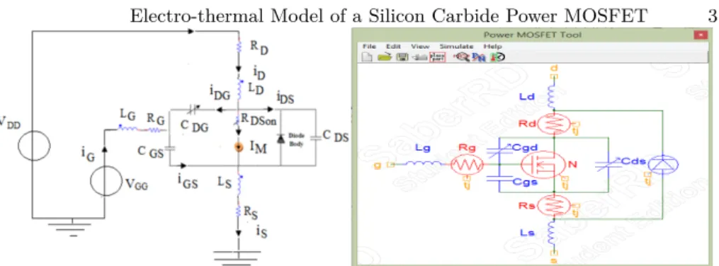
The electrical model of a SiC MOSFET (25𝑚𝛺,1200𝑉 and 90𝐴) proposed here is based on the EKV’s one. The power losses are analysed to estimate and take into account their effect as shown in the equivalent scheme of Fig. 1. 𝑉𝑆, 𝑉𝐺 et
𝑉𝐷 are respectively the Source, Gate and Drain voltages. It includes 3 parasitic
inductances (connected in series with the transistor electrodes 𝐿𝐺, 𝐿𝐷, 𝐿𝑆) to
describe the behaviour at high frequencies and the commutation losses. The resistance 𝑅𝐺 estimates the gate losses. These inductances and the resistances
are used to estimate the power losses during the switching [7–9]. The different variables and parameters (𝑉𝐷𝑆, 𝐼𝐷𝑆, 𝑅𝑑𝑠𝑜𝑛,. . . ) of the model vary also in function
of the junction temperature [10].
In this model, we used parameters from the datasheet and the others from an optimization (comparison) that was performed by Saber, Psim and PSpice. Fig. 1 shows the EKV deduced scheme for a SiC MOFET developed under the softwares. The EKV model is based on mathematical expressions which accounts for a MOSFET operation in three regions. It is composed of two current sources G1 and G2. For interpolation between these regions of operation, a linear combination of logarithmic functions is used by EKV.
Electro-thermal Model of a Silicon Carbide Power MOSFET 3
Fig. 1. Electric model of the SiC MOSFET (C2M0080120D) in Saber Software The specific current is 𝐼𝑠0 = 2.𝑈
2
𝑡ℎ.𝐾𝑠.𝑔𝑚. The Drain-Source current (𝐼𝐷𝑆),
in the EKV MOSFET model [7, 8], is defined by equation 4, as the difference beetwen the direct 𝐼𝐺1(2) and the reverse one 𝐼𝐺2 (3) [6].
𝐼𝑀 = 𝐼𝐺1(𝑉𝑝− 𝑉𝑆) − 𝐼𝐺2(𝑉𝑝− 𝑉𝐷) (1) 𝐼𝐺1= 𝐼𝑠.𝑔𝑚. [︂ 𝐿𝑛(1 + 𝑒𝑥𝑝𝑉𝑝− 𝑉𝑠 2𝑉𝐷𝑆 ) ]︂2 (2) 𝐼𝐺2= 𝐼𝑠.𝑓 𝑡. [︂ 𝐿𝑛(1 − 𝑒𝑥𝑝𝑉𝑝− 𝑉𝐷 2 ) ]︂2 (3) 𝐼𝑀 =2𝜆𝑈𝑡ℎ2𝐾𝑠𝑔𝑚((𝐿𝑛(1 + 𝑒 𝑉𝑝−𝑉𝑠 2𝑉𝐷𝑆 ))2− 𝑓 𝑡(𝐿𝑛(1 − 𝑒𝑉𝑝−𝑉𝐷2 ))) (4) where 𝑔𝑚is the transconductance, 𝐾𝑠 is the slope factor, 𝑉𝑝= (𝑉𝐺𝐾−𝑈𝑡ℎ)
𝑠 the
pinch voltage with 𝑈𝑡ℎthe thermodynamic reference voltage and 𝑓𝑡 the internal
thermal voltage. This model of Fig. (1) can then be used for simulation and prototyping of any application using this SiC MOSFET into softwares like Saber, Pspice, Psim (see section 3) or Matlab/Simulink (see [11]). The electric equivalent scheme can be completed by electric equations to allow any kind of its numerical simulation.
In a second step, we can consider and include, to this model, the parameters temperature dependance. The accuracy of the proposed model will be enhanced by modeling of the influence of temperature on electrical parameters.
The variation of the junction temperature, leads to parameters variation which can be described as follows, where 𝜗 = −8.5𝑚𝑉/°K. The variations included in the previous model show that the model is Non Linear and Time Varying (NLTV). 𝑉𝐺𝑆(𝑡ℎ)(𝑇𝐽) = 𝑉𝐺𝑆(𝑡ℎ)(300°𝐶) + 𝜗.(𝑇𝑗−300°C) 𝑔𝑚(𝑇𝑗) = 𝑔𝑚(300°𝐶)( 𝑇𝑗 300) −1.5 𝑅𝐷𝑆𝑂𝑁(𝑇𝑗) = 𝑅𝐷𝑆𝑂𝑁 (300°C)(1 +100𝛼 ) (𝑇𝑗−300) (5) It remains now to describe the temperature variations by a dynamic model which takes into account the MOSFET operation and convert the power losses in heating the component. Thermal dynamic behaviour is obtained using the heat equation and the finite element method.
2.3 Thermal Model
The electro- thermal coupling between the electrical parts and the thermal parts is produced by the power losses 𝑃𝑃 dissipated during normal operation. This
power can be estimated by the following equations [8, 9]:
𝑃𝑃 = 𝑅𝐷𝑆𝑜𝑛(𝑇 ).𝑖2𝐷𝑆+ (0.25.𝛥𝑡.𝐹.𝑉𝐷𝑆.𝑖𝐷𝑆) (6)
We have used the Finite Element Method (FEM) based on an RC Cauer network. As also used in Pspice simulation, we have considered 14 cells of (𝑅, 𝐶) equivalent components (Fig.(2) [9]. It gives a very good global approximation of the thermal behaviour going from the MOSFET junction temperature 𝑇𝑗 to the
ambiant air temperature 𝑇𝑎 (assumed to 25°C), through the case (𝑇𝑐) (package
and the thermal dissipation radiator, 𝑇𝑟) (see Fig.(2)).
Fig. 2. Thermal model of SiC MOSFET
The RC layers describing the heat flow has as input power loss to be dissipated as an equivalent current source and as second output the ambiant temperature 𝑇𝑎
represented by voltage source (see Fig. 2). The ouptut of interest is of course the junction temperature 𝑇𝑗. A 𝑉𝑎= 25𝑉 continuous voltage source correspond to
the ambiant air temperature 𝑇𝑎= 25°𝐶. The flow of the dissipated power losses
is represented by an input current source (𝑃𝑃). The junction temperature 𝑇𝑗 is
imposed trough the thermal impedance 𝑍𝑇 𝐻 between the MOSFET junction
and the ambiant air and the dissipated power losses (𝑃𝑃) by the heat transfer
equation 𝑍𝑇 𝐻 = 14 ∑︁ 𝑖=1 𝑅𝑖*(1 − 𝑒𝑥𝑝𝑅−𝑡𝑖𝐶𝑖) 𝑇𝑗= 𝑇𝑎+ 𝑃𝑃* 𝑍𝑇 𝐻 (7)
The thermal MOSFET behaviour, if we consider the thermal state vetor
𝑋𝑇 = [𝑇𝑗, 𝑇1, ..., 𝑇14, 𝑇𝑟] 𝑇 can be expressed as ⎧ ⎪ ⎪ ⎪ ⎪ ⎪ ⎪ ⎪ ⎪ ⎪ ⎪ ⎪ ⎪ ⎨ ⎪ ⎪ ⎪ ⎪ ⎪ ⎪ ⎪ ⎪ ⎪ ⎪ ⎪ ⎪ ⎩ 𝑇1= 𝑇𝑗− 𝑅1 (︀ 𝑃𝑃 − 𝐶1𝑑𝑇𝑑𝑡𝐽 )︀ 𝑇2= 𝑇1− 𝑅2(︀𝑃𝑃 − 𝐶1𝑑𝑇𝑑𝑡𝐽 − 𝐶2𝑑𝑇𝑑𝑡1)︀ 𝑇3= 𝑇2− 𝑅3(︀𝑃𝑃− 𝐶1𝑑𝑇𝑑𝑡𝐽 − 𝐶2𝑑𝑇𝑑𝑡1 − 𝐶3𝑑𝑇𝑑𝑡2)︀ 𝑇4= 𝑇3− 𝑅4(︀𝑃𝑃− 𝐶1𝑑𝑇𝑑𝑡𝐽 − 𝐶2𝑑𝑇𝑑𝑡1 − 𝐶3𝑑𝑇𝑑𝑡2− 𝐶4𝑑𝑇𝑑𝑡3)︀ : : : : : : : : : : : : : : : : : 𝑇𝑁= 𝑇𝑁 −1− 𝑅𝑁 (︁ 𝑃𝑃 − 𝐶1𝑑𝑇𝑑𝑡𝐽 − 𝐶2𝑑𝑇𝑑𝑡1 − ... − 𝐶𝑁 𝑑𝑇𝑁 −1 𝑑𝑡 )︁ 𝑇𝑟= 𝑇𝑁+1= 𝑇𝑁− 𝑅𝑅 (︀ 𝑃𝑃− 𝐶1𝑑𝑇𝑑𝑡𝐽 − ... − 𝐶𝑁𝑑𝑇𝑑𝑡𝑁 )︀ 𝑇𝑎= 𝑇𝑟− 𝑅 (︁ 𝑃𝑃− 𝐶1𝑑𝑇𝑑𝑡𝐽 − ... − 𝐶𝑁+1 𝑑𝑇𝑁 +1 𝑑𝑡 − 𝐶 𝑑𝑇𝑟 𝑑𝑡 )︁ (8)
Electro-thermal Model of a Silicon Carbide Power MOSFET 5
3 Simulations Tests and Model Validation
The developed model has been implemented in Saber, Pspice and Psim softwares and compared to the experimental curves presented by the SiC MOSFET data sheet for its validation.
3.1 Saber Simulation Model
The proposed model is then implemented under Saber software (see Fig. 1). The use of Power MOSFET Tool and the Diode Tool proposed in Saber allow us to extract the SiC MOSFET parameters and get curves using fitting to optimize the estimation errors. The verification of the output characteristic 𝐼𝐷𝑆 = 𝑓(𝑉𝐺𝑆)
with the Saber optimized simulation model, for 𝑇𝑗= 25∘𝐶 and 𝑇𝑗 = 150∘𝐶as
proposed and developed in this work, is shown in Fig. 3.
Fig. 3. 𝐼𝐷 current versus 𝑉𝑑𝑠
The Fig. 3 compares the variation of the current 𝐼𝐷𝑆 as a function of the
voltage 𝑉𝐺𝑆 for a voltage 𝑉𝐷𝑆 = 20𝑉 and a junction temperature of 25 °C (left
curve) and 150°C (right) to the curves got from the datasheet (dotted line).
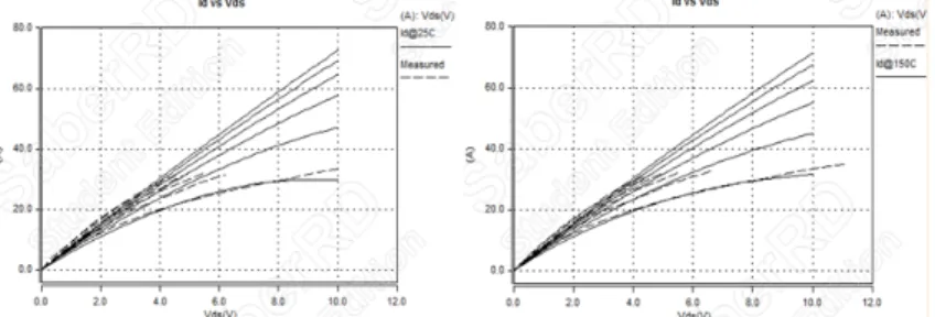
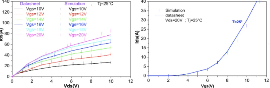
Fig. 4. Id current in function of 𝑉𝐷𝑆 for different 𝑉𝐺𝑆 values
The Fig. 4 compares the variations of the current 𝐼𝐷𝑆 versus 𝑉𝐷𝑆 for different
𝑉𝐺𝑆 values and the same junction temperature of 25 °C (left curve) and 150°C
(right) to the curves got from the datasheet (dotted line). Among this experiment we got respectively for 25°C and 150°C, a threshold voltage 𝑉𝑡ℎ= 3.808𝑉 and
𝑉𝑡ℎ= 2.313𝑉 , Drain resistance 𝑅𝑑= 0.1𝛺 and 𝑅𝑑 = 0.0942𝛺, Source resistance
𝑅𝑠= 0.01033𝛺 and 𝑅𝑠= 0.0173𝛺 and Gate resistance 𝑅𝑔= 4.6𝛺 and 𝑅𝑔= 4.6𝛺
Fig. 5. I-V Charasteristic for 𝑇𝑗= 25∘𝐶and 𝑇𝑗= 150∘𝐶
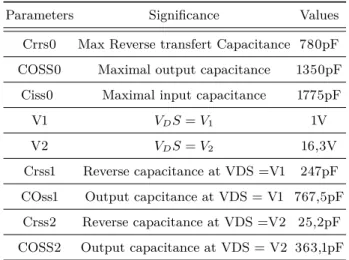
The current versus output voltage (I-V) characteristics of the integrated diode has also been compared, using Diode Tools of Saber software. Results are represented in Fig. 5. The capacitance curves of datasheet have also been fitted to get the MOSFET model parameters. For two 𝑉𝐷𝑆 values V1 and V2 we got
the parameters values summarized in Fig. 1.
Parameters Significance Values Crrs0 Max Reverse transfert Capacitance 780pF COSS0 Maximal output capacitance 1350pF
Ciss0 Maximal input capacitance 1775pF
V1 𝑉𝐷𝑆= 𝑉1 1V
V2 𝑉𝐷𝑆= 𝑉2 16,3V
Crss1 Reverse capacitance at VDS =V1 247pF COss1 Output capcitance at VDS = V1 767,5pF Crss2 Reverse capacitance at VDS =V2 25,2pF COSS2 Output capacitance at VDS = V2 363,1pF
Table 1. MOSFET estimated Parameters
A comparison of the Gate charge, Gate threshold voltage, ON-state resistance and transconductance are given in Table 6. We then got :
- A very good agreement between the simulations represented by continuous lines and those of datasheet represented by a points,
- For gate voltages 𝑉𝐺𝑆 lower than 3.8V, the MOSFET is switched OFF because
the condition 𝑉𝐺𝑆 is not greater than or equal to that transistor threshold 𝑉𝑡ℎ.
Beyond 3.8V, the MOSFET starts to operate and the current 𝐼𝐷𝑆 gradually
increases.
3.2 PSpice simulation Model Validation
Several simulation results obtained, using the model implemented under the Pspice software, were compared with those of the datasheet of the CREE’s
Electro-thermal Model of a Silicon Carbide Power MOSFET 7
Fig. 6. Comparative results and the Psim model
MOSFET [9]. The model scheme is given in Fig. 7 with the parameters estimated (under Pspice tests) from datasheet. We can note that the resistances 𝑅𝑑 and 𝑅𝑠
are small and have been neglected.
Fig. 7. Pspice Sic MOSFET C2M0080120D and Parameters
The Fig. (8) below show good behaviour of the electrothermal model proposed in this work. Fig. 8 represents the variation of the Drain-Source current (𝐼𝐷𝑆) as
a function of the voltage at the output of the SiCMOSFET (𝑉𝐷𝑆) for different
Grid-Source voltage values (𝑉𝐺𝑆) and a temperature of 25°C. It appears that
there is a very good agreement between the simulation results, represented by lines, and those of datasheet, represented by poinctual bars.
Fig. 8. Variation of 𝐼𝐷𝑆 current versus 𝑉𝐷𝑆 for different values of 𝑉𝐺𝑆
Fig. 8 the variation of the current 𝐼𝐷𝑆 as a function of the voltage 𝑉𝐺𝑆
for a voltage 𝑉𝐷𝑆 = 20𝑉 and a temperature of 25 ° C. We can note a very
good agreement between the simulation results represented by continuous lines and those of detasheet represented by dotted bars. For voltages 𝑉𝐺𝑆 < 4𝑉 ,
the MOSFET is not controlled because the condition 𝑉𝐺𝑆< 𝑉𝑡ℎ, the treshold
condition is not verified. Beyond 4V, the transistor start to operate and the current
𝐼𝐷𝑆 gradually increases. Fig. 9 show the thermal effect on the Drain-Source
resistance (𝑅𝐷𝑆𝑜𝑛) compared to the datasheet characteristic, for 𝐼𝐷𝑆 = 50𝐴 and
𝑉𝐺𝑆= 20𝑉 . It appears that the electro thermal model developed in this work
has a high accuracy and is close to actual operating (datasheet) up to very high temperatures (150°C).
Fig. 9. 𝑅𝐷𝑆𝑜𝑛Variations in function of the junction temperature
In summary, the electric model developed, under Pspice, during this work has considerable precision. This allows us subsequently to use this simulation model in the power electronics to clearly show these performance and advantages over silicon transistors. Although the CREE model fairly accurately represents the evolution of 𝑅𝐷𝑆𝑜𝑛 in function of the junction temperature, it has some
discrepancy with the datasheet. However, with our simulation model, it is easy to see a better superposition between the two curves by adjusting the coefficients mentioned in Table 1.
3.3 Psim simulation Model Validation
The proposed model is implemented in Psim software as described by the Fig. (6). The improvements in the simulation model need additional adjustments of the device characteristics and computation parameters such as variable simulation step size which is used for the convergence rapidity. For our SiC MOSFET, we use the parameters that have been extracted from the data sheet (see table 7). The Drain and Source resistances have been neglected. The Fig. 10 shows the variation of 𝐼𝐷𝑆 in function of the drain-source voltage 𝑉𝐷𝑆. It compares
the Drain-Source current (𝐼𝐷𝑆) versus the MOSFET output voltage (𝑉𝐷𝑆) for
several Gate-Source voltages (𝑉𝐺𝑆) under a temperature of 25°C. The simulated
characteristics are then compared to the data sheet values and curves. Simulation results (continuous lines) are in good agreement with the data sheet values (dots).
The Fig. 10 shows the variation of 𝐼𝐷𝑆 in function of the Gate-Source voltage
Electro-thermal Model of a Silicon Carbide Power MOSFET 9
Fig. 10. 𝐼𝐷𝑆 versus 𝑉𝐷𝑆 for different 𝑉𝐺𝑆 values
and 𝐼𝐷𝑆 versus 𝑉𝐺𝑆 for 𝑇𝑗25°C and 150°C
𝑉𝐺𝑆 values less than 4V, the MOSFET is not controlled because the threshold
voltage 𝑉𝑡ℎis not reached. When the MOSFET start operation 𝑉𝐺𝑆> 𝑉𝑡ℎ>4𝑉 ,
and then the current IDSincreases gradually with 𝑉𝐺𝑆. The results are in good
agreement.
Fig. 11. Variation of 𝑅𝐷𝑆𝑜𝑛versus the temperature Tj
The Fig. 11 shows the simulated and the actual Drain-Source resistance (𝑅𝐷𝑆𝑜𝑛) in function of the temperature variation 𝑇𝑗, for a current equal to
𝐼𝐷𝑆 = 50𝐴 and voltage VGS=20V. The obtained curves are very close in a wide
temperature range (up to T=150°C). We observe that the result obtained is similar to the datasheet, particularly in the interval [0∘𝐶,150∘𝐶].
4 Conclusion
A new model of SiC Power MOSFET is proposed in this paper. This model is implemented successfully under Psim, Pspice and Saber softwares and then have been tested and optimized for numerical circuit design and simulation. The Characteristics of the MOSFET simulation models (on-state resistance, threshold voltage, and transconductance, etc...) has been compared to actual characteristics given by manufacturer’s data sheet in Psim, PSpice and Saber.
The proposed electrothermal model is very accurate and able to describe the dynamic behavior of the SiC MOSFET with a very good precision. Owing to our last results, it is shown that the electrothermal model developed on Psim, Pspice
an Saber has a high accuracy and is close to the optimum operating conditions presented in the datasheet. This simulation model of SiC power MOSFET is easy to use in numerical design and prototyping of electric circuits and simulations. The future work of our staff will be on nonlinear and robust control of a power circuit including the SiC MOSFETs.
Acknowlegment
This research is activity is held by the SASV group of the LSIS- UMR CNRS 7296 and co funded by the BPI in an FUI project. Special aknowledgements are addressed to all the PFC Ranger project partners. The authors (member R22190) would like to thanks also Europractice (http://www.europractice.stfc.ac.uk/ )
References
1. H. C. Foong, Y. Zheng, Y. K. Tan, and M. T. Tan, “Fast transient integrated digital DC DC converter with predictive and feedforward control,” vol. 59. 1
2. N. Bejoy, N. Pushpakaran, B. Stephen, B. Bayne, G. Wang, and J. Mookken, “Fast and accurate electro-thermal behavioral model of a commercial sic 1200v, 80 mohm power mosfet,” IEEE Transactions on Electron Devices, january 2015. 1
3. B. Pushpakaran, S. Bayne, G. Wang, and J. Mookken, “Fast and accurate electro-thermal behavioral model of a commercial sic 1200v 80 mohms,” IEEE Pulsed Power Conference (PPC), December 2015. 1
4. B. Wang and Y. Ma, “Research on the passivitybased control strategy of buck-boost converters with a wide input power supply range,” n Power Electr. for Distrib. Generat. Syst, vol. 13, 2010. 1
5. E. Vittoz, C. C. Enz, and F. Krummenacher, “A thermal characterization of power transistors semiconductor,” vol. 11. 1
6. Stefanović, Danica, and M. Kayal, “Bsim to ekv conversion,” 01 Bsim To Ekv Conversion. 1
7. L. Juejing, K. Sun, W. Hongfei, Y. Xing, and L. Huang, “Modeling of sic mosfet with temperature dependent parameters and its applications,” in Twenty-Eighth Annual IEEE Applied Power Electronics Conference and Exposition, A. 2013, Ed., 2013, pp. 540–544. 2.2, 2.2
8. F. Bilbao, B.Argenis, and L.Stephen, “Pspice modeling of silicon carbide mosf ets and device parameter extraction,” in IEEE InternationalPower Modulator and High Voltage Conference,. PMHVC 2012, 3-7 June 2012, pp. 776–779. 2.2, 2.2, 2.3 9. CREE, “Sic power mosfet cmf20120d datas-sheet and application note,” http://www.
cree. com/products/pdf/CMF20120D. pdf, 2015. 2.2, 2.3, 2.3, 3.2
10. T. M. Nutt, A. Hefner, H. Mantooth, J. Dultiere, D. Berning, and R. Singh, “Parameter extraction sequence for silicon carbide schottky, merged pin schottky and pin power diode models,” Power Electronics Specialists Conference, vol. 3, February 2002. 2.2
11. N. K. M’Sirdi, A. Naamane, K. Frifita, M. Boussak, and E. Baghaz, “State space models nltv for electro-thermal behaviour of a power sic mosfet,” submitted to ICEERE2018, Saidia Oujda Morroco, April 2018. 2.2