Development of a laboratory course in power electronic control
circuitry based on a PWM buck controller
by
Candace N. Wilson
Submitted to the Department of Electrical Engineering and Computer Science in Partial Fulfillment of the Requirements for the Degrees of Bachelor of Science in Electrical
Science and Engineering and Master of Engineering in Electrical Engineering and Computer Science at the
MASSACHUSETTS INSTITUTE OF TECHNOLOGY May 26, 2006
© 2006 Massachusetts Institute of Technology
Author I
Department of Electrical Engineering and Computer Science May 25, 2006
Certified by
Professor of Electrical Engineering and
Steven B. Leeb Computer Science Thesis Supervisor
Certified by
Al-Thaddeus Avestruz PhD Candidate. LeDartment ot blectncai LnmneerinQ and Computer Science Thesis Supervisor
Accepted by
"OFH cEOtOOGY
AUG
1420Development of a laboratory course in power electronic control
circuitry based on a PWM buck controller
by
Candace N. Wilson
Submitted to the Department of Electrical Engineering and Computer Science May 2006
In Partial Fulfillment of the Requirements for the Degrees of Bachelor of Science in Electrical Science and Engineering and Master of Engineering in Electrical Engineering
Abstract
Due to the constraints on time and resources within the typical electrical engineering curriculum, it is difficult for students to obtain Integrated Circuit design experience prior to entering industry. This project establishes the foundation for a new laboratory course in power electronics and analog circuit design. There is an introduction to power electronics, particularly the buck converter, and several basic analog circuit building blocks are introduced. A process consisting of circuit design, simulation, construction, and evaluation is developed to provide students with an introduction to Integrated Circuit design. A peak current mode PWM controller for a buck converter is developed to illustrate the fundamental power electronic and analog circuit concepts that are presented.
Thesis Supervisors:
Steven B. Leeb, Professor of Electrical Engineering and Computer Science Al-Thaddeus Avestruz
Contents
1 Introduction... 2
2 Background ... 4
2.1 Buck Converter ... 4
2.2 Control ... 13
2.3 PWM Controller Using Commercial Integrated Circuits ... 31
3 Analog Circuit Blocks... 40
3.1 Current Sources... 40
3.2 Com m on Em itter Am plifier... 49
3.3 Em itter Follow er Buffer... 52
3.4 D ifferential Pair ... 55
4 Control Circuit Blocks ... 66
4.1 Bandgap Reference ... 66
4.2 Operational A m plifier ... 83
4.3 Com parator ... 93
4.4 Clock... 99
4.5 Error Am plifier ... 105
4.6 Current Sense Am plifier ... 109
4.7 Logic and RS Latch ... 117
4.8 Leading Edge Blanking... 121
4.9 G ate D rive ... 126
4.10 Protection Circuits ... 138
5 Results... 147
6 References... 153
7 Appendix... 154
7.1 CM O S Com binational Logic G ates ... 154
7.2 EAGLE Schem atics ... 158
1 Introduction
Companies are discovering that often new electrical engineering graduates have very limited knowledge about the integrated circuit (IC) design process. As a result, the initial training period is longer and more extensive than desirable. This is largely because it is fairly challenging to duplicate the intricacies of the IC design process within the resource and time constraints of a typical electrical engineering curriculum.
Additionally, it is difficult to remain informed of changes continually developing in industry and to expose students to the many practical concerns involved. This document describes an attempt to create a reasonable and feasible way to make the classroom experience more effective in terms of providing insight and understanding of the IC design process.
This project has developed the foundation for a new laboratory course. The objectives of the new course include the following: 1) introduce students to the fundamentals of power converter control theory, 2) teach students to design analog control circuitry block by block, 3) teach students to simulate models of their circuit designs, 4) instruct students on how to build and debug their circuits and compare experimental results with the simulated results. Ideally, the students will obtain
something close to the IC design experience, although they will be using discrete components and constructing on a breadboard or a pre-designed PC board with sockets for inserting components.
The following is a brief overview of the structure of this document. Section 2 contains the power electronics background information required to establish the context for the circuit designs. The buck converter is presented and its general operation is
explained. There is a brief introduction to control theory. Transfer functions are developed for the buck converter and the converter's stability in a closed-loop
configuration is addressed. Additionally, in this section the requirements for a PWM control circuit are discussed and an IC version, designed with common commercial operational amplifiers, comparators, and other chips, is developed. Section 3 deals with basic analog circuit building blocks. Commonly used circuits, such as current sources, common emitter amplifiers, and differential pair amplifiers, are introduced and analyzed in detail. Section 4 provides a description of each of the control circuit's functional blocks. Each block is explained and a transistor-level circuit is designed and analyzed. Section 5 contains a brief summary of the project and conclusions and results are formulated. Section 6 is an appendix consisting of diagrams and truth tables for combinational logic gates as well as the full EAGLE schematics for all of the circuit blocks presented in Section 4 as they are laid out on the PC board for the laboratory kits.
2 Background
2.1 Buck Converter
The buck converter is being used as the framework for our converter and controller design. A buck converter is a DC-to-DC power converter which takes some DC input voltage and produces a lower DC output voltage. Figure 2-1 shows the general structure of a buck converter. It consists of 2 switches (SI and S2) which are controlled
concurrently such that when S, is on (closed), S2 is off (open), and vice versa. This control is typically periodic with some period T, where T
=
withfs representing thefs
switching frequency.
LI
SL R
IYi -- Vaut
Figure 2-1. Buck converter schematic.
The fraction of the period during which Si is on is referred to as the duty ratio or duty cycle (D). The voltage at the node between Si and S2, Vm, is Vin when Si is on and
zero when S2 is on, as indicated in Figure 2-2. The upper waveform in Figure 2-3 shows
an example of what Vm looks like in practice. Note that a significant amount of ringing in the waveform can be observed at the start of every cycle. The inductor (L) and
DC component of Vm and blocks the AC component. The second-order LC filter effectively averages Vm to produce the converter's output voltage:
SVin -DT+O-(1 T S,
state
on
-off__ _ 0DT
T T+DT
t -D)T D. (2.1)Vin
<Vm> =DVn
(...)JI
I_
DT T T+DT t NOTICE: Vdc VacDV
int
<Vac> =0!
C..)
.-.-..- t DT TFigure 2-2. Voltage, Vm, at the midpoint between the converter's switches.
The constituitive relation for an inductor is
diL VL =L .i
dt (2.2)
V
Thus, when the voltage across the inductor is positive, the inductor current is increasing and when the voltage is negative, the current is decreasing. During the first part of the cycle, when S1 is on, the voltage across the inductor is
VL =Vl -Vin , (2.3)
This is a positive voltage because Vout is less than Vin (by definition) so the inductor current is ramping up. During the second part of the cycle, the inductor voltage is
VL = = -VO, . (2.4)
This is a negative voltage, thus the inductor current is ramping back down. In
equilibrium, the average inductor current is constant, meaning the current must ramp up and down equal amounts. The lower waveform in Figure 2-3 is of a buck converter's inductor current in equilibrium. We can solve (2.2) for diL to obtain an expression for the inductor current ripple.
v Lt
AiL = (2.5)
1.0V tM400IS A Ch4fI52mA
Ch4 2OOmA( ,
Figure 2-3. Voltage between buck converter switches and inductor current waveform
When designing a buck converter, we typically have some specification for the maximum allowable inductor current ripple. Given the current ripple spec and the inductor voltage expressed in either (2.3) or (2.4), we can derive a constraint that specifies the minimum value inductance required. Solving (2.5) for L yields the inequality
(2.6a)
V L_* At AiL
During the first part of the cycle, when Si is on, we can substitute (2.3) for vL and DT for At to obtain
L> (V -V,, -, DT
AiL
The inductor current ripple shows up as ripple in the output voltage. We can assume that the entire ripple current flows through the capacitor. See the graph of capacitor current in Figure 2-4. The charge injected into the capacitor when the current ripple is positive is I Ai T q 2 . (2.7a) Simplification yields 1 q =- . Ai-T. 8 (2.7b)
From the capacitor's constituitive relation, we obtain the following equation for voltage ripple as a function of injected charge
(2.8) Av =q
C
Substituting the expression from (2.7) for q in (2.8) gives us an expression for voltage ripple as a function of the inductor current ripple.
Ai*-T Av =
Given a spec for the maximum allowable voltage ripple, we can solve (2.9) to determine the required value for C.
C Ai.T (2.10) 8 -Av
I.
(z)
Total
charce
DT
--tFigure 2-4. The inductor current ripple flows through the capacitor. This ripple current can be integrated to determine the total charge that enters the capacitor.
There are two options for the implementation of the buck converter's switches. We can either use MOSFETs for both switches (synchronous rectification), or we can use a MOSFET for SI and implement S2 with a free-wheeling diode. The second
diode to conduct when S1 is turned off. Examples of these switch implementations are contained in Figure 2-5. If we use synchronous rectification, we need a delay circuit, similar to the one shown in Figure 2-6, to ensure that the switches are never on at the
same time.
HB L
15 Volts C R
T-PWM Control POT for Duty
Cycl eA/olume Adjust
L
15
Volts
-RPWM Control
POT for Duty
CyleVolume Adjust
Figure 2-5. The lower switch of a buck converter can be implemented either with a MOSFET or a diode.
D
a[ C_ R 13 1DEELY
V2 V3 V4 V
R0 DELAY
Figure 2-6. A delay circuit is required to ensure that both switches are not on at the same time when the converter's lower switch is implemented with a MOSFET.
For the case when S2 is implemented with a diode, it is possible for the inductor
current to ramp all the way down to zero, at which point the switch will turn off. This is referred to as discontinuous conduction mode (DCM). In order to ensure that this never happens (meaning the converter operates in continuous conduction mode, CCM), the inductor current ripple is not more than twice the average inductor current. Figure 2-7
shows graphically how to determine the requirements for CCM.
i (t)
Ai (V * At)/L
<Op) =Iaoad
t
D T T
Figure 2-7. Graphical representation of the inductor current at the boundary between CCM and
DCM operation.
The boundary between DCM and CCM is when the average inductor current, which is the same as the load current, is equal to half of the inductor current ripple. This condition is expressed mathematically as
('L ='Load = Ai -(2-11)
iL = iLoad > -.i (2.
2
For a resistive load,
V(2
iLoad
-(2.
R
Combining (2.12) and (2.13) yields
Ai < " (2.
R
as the requirement for CCM. Substituting the expression for Ai contained in (2.5) and solving for L gives us the minimum inductance required for the converter to remain in continuous conduction mode.
VL At.R (2.
2 -V
Again, using the values for the first part of the switching cycle, (2.15) becomes
(V,1 -Vou) -DT -R 2 -Vo 12) 13) 14) 15) 16)
2.2 Control
The buck converter's output voltage is proportional to both the input voltage and the duty ratio at which its switches are operated. This relation, expressed mathematically in (2.1), is repeated here in (2.17).
V =Vi, D (2.17)
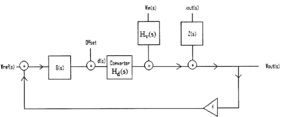
So for a given input voltage, one can set D so that the converter produces the desired output voltage. However, if the input is from an unregulated supply or its value varies over some range, we need a control circuit that manipulates the duty ratio in response to variations in Vin in order to maintain a constant output voltage. . This requires a feedback loop, so that information about the output voltage can be sent to the control circuit. Feedback allows the controller to sense whether the output is too high or too low
so it can send the appropriate corrective signals to the converter's switches. Figure 2-8 shows an example of a buck converter with simple control loop. The operational
amplifier (op amp) computes the error between the converter's output and some reference voltage then amplifies the error by some factor, K. A comparator then compares the amplified error with a triangle wave and outputs a pulse of variable width. The width of the pulse is determined by the fraction of the period, T, set by the triangle wave that the op amp's output is greater than the level of the triangle wave. That fraction determines the duty ratio at which the switch is operated. This is known as Pulse Width Modulation, or PWM, control.
vout
+
I IK(vref - vout)
PWNI Op amp Comparator I Vref ( M) T 2T 3T 4TFigure 2-8. Buck converter with a PWM control loop.
In addition to regulating Vout, we may be interested in controlling the output (and inductor) current. This can be accomplished by placing a small resistor between the input and Si and using the voltage across this current sense resistor to estimate and constrain the inductor current. This is known as peak current mode control because when the current reaches a predetermined maximum level, the controller turns Si off regardless of Vout. At this point the inductor current ramps down until the start of the next cycle. See Figure 2-9 for an example of a current-mode control circuit for a buck converter. The artificial ramp provides slope compensation which is discussed in detail towards the end
Vin
L
VmT
D
/out(K AV
)
Vi
of this section. The other blocks in the control circuit are introduced in Section 2.3 and covered more extensively in Section 4.
1)0
I (3arto
. ... a m 'Po
mp-it
Figure 2-9. Buck converter with current-mode controller.
Modeling the Converter
Before we can design a control loop for the converter, we must have a model of the converter from which we can derive a transfer function. We can develop a linear,
model for a buck converter with voltage mode (duty ratio) control is contained in Figure 2-10.
L
f D)=D*Vin R
+ __ Vout
Figure 2-10. Averaged model for buck converter.
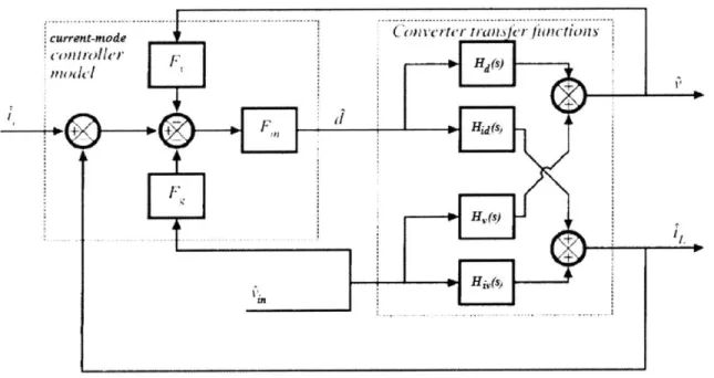
There are a few different transfer functions to consider when modeling a
converter. The line-to-output transfer function, H, (s), describes changes in the output voltage due to changes in the input voltage. The control-to-output transfer function,
Hd (s), describes changes in the output voltage due to changes in the duty cycle control variable. The output impedance, Z,, (s), describes changes in the output voltage due to changes in the load current. We are also concerned with the inductor current. The transfer function, Hd (s), describes changes in the inductor current due to changes in d and Hiv (s) is the transfer function describing changes in inductor current due to changes in the input voltage. These important transfer functions are derived for the buck
H,(S)= vou,
(S)
vin (s) H,(S)= D L (2.18) s2LC+s +1 R d(s) Vout Hd(S) D L (2.19) s2LC+s-+1 R iZs= (s) isL Zut (s)= sL L (2.20) s 2LC+s-+1 R (idS)iL (S) H i s d(s) Hid (s)= V"" (1+ sRC) (2.21) D-R(s2LC+s R +1)Hv
(S)=
'i(s) vin (s)D(1+sRC) (2.22)
R(s2LC+s-L +I R
Figure 2-11 shows the block diagram for a voltage-mode control loop.
Figure 2-11. Voltage-mode control loop block diagram.
If peak current mode control is used, the switches and inductor can be modeled as a dependent current source with duty ratio as a parameter. This model is shown in Figure 2-12. In this case, the transfer function from input to output voltage becomes
V R
H (s) = V"' (s) = . (2.23)
Controlling the peak current simplifies the model from second order to first order (i.e. 1 pole instead of 2).
I =g (D)
I
I
-
RVout
Figure 2-12. Averaged Model for Peak Current-Mode Control.
The complete set of transfer functions for the current-mode control case as derived in [1] are contained in (2.24)-(2.28). H Vs.(s) ic(s) Hi(S)=- FGvd 1+ F,(Gid+ FGd) H (S)- v,(s) vic (s) CM H, -FmFHd +Fm(HvGi-GjvHd) nv-m ks) = I+Fm(Gid -FHd) (2.24) (2.25)
The new variables introduced in (2.24) and (2.25) are defined for a buck converter as Fg 2Lf, S(1- 2D) 2Lf, F'" Ma
(2.24) and (2.25) can be normalized as shown in (2.27) and (2.28)
Hi(S)= 2 Ge
C
HV-CM(S)=- ) Ggo + s +1 OC + QC where _ V Fm D F,,FVm
V + FV+1
' D DR (2.26) (2.27) (2.28)1 Fm F V FV w =±m +1, C D DR
Fm
FvV FmV C P+ +1 Q=CR D DR L RCFM '"+1+ DL I-F, Fg V1-
mn g G go=D Fm$FV FmV + +1I D DRFigure 2-13 shows the block diagram for a current-mode controller.
current-mode C i verle r s J t
Ifl/Odd
H (A
Compensation
An error amplifier must be designed to provide some compensation, G(s), to ensure that the overall system is stable. Stable is defined as input bounded-output (BIBO) stability, meaning any bounded input to the system produces a bounded output. It typically is not enough just to know that a system is stable. It is often critical to know how stable and how accurate the system is. Phase margin is used to indicate degree of stability. It is defined as the difference between the phase of the system and
-180 degrees at the frequency when the magnitude response is equal to 1. This frequency is referred to as the crossover frequency. Generally, increasing the phase margin makes the system more stable. Given the phase margin, various stability criteria such as peak overshoot in the step response, rise time, settling time, and peaking in the frequency response magnitude can be determined. A system's response speed is measured in bandwidth. Higher crossover frequency corresponds to higher bandwidth. Steady-state error is used as a measure of the system's accuracy. Steady-state error is the difference between the command signal (for example, the reference voltage) and the feedback signal. This indicates how well the output is following the reference.
Disturbance rejection refers to the system's ability to reject disturbances in the forward path. Good disturbance rejection is accomplished by introducing high gain in the loop transfer function at low frequencies. Noise rejection is a measure of the system's insensitivity to high frequency noise. Good noise rejection is obtained by significantly attenuating the magnitude of the loop transfer function at high frequencies. Refer to [3] for an introductory treatment of control theory.
There are numerous methods of compensation. The simplest is proportional control, meaning the compensator is just some constant gain: G(s) = K. Proportional control can be used to stabilize a system by increasing its phase margin, but the system's bandwidth is decreased. There is a tradeoff. Using proportional control, one can't be improved without degrading the other. Additionally, lowering the gain to stabilize a system decreases the disturbance rejection and increases the steady state error. Another option is dominant pole compensation, where the compensator introduces a low
frequency pole to force crossover before the phase becomes too negative. This method also lowers the magnitude and decreases bandwidth. Depending on the application, speed may not matter and proportional or dominant pole compensation may be adequate.
Lag and Lead compensation are methods that provide a bit more flexibility than the ones previously mentioned. Lag compensation adds a low frequency pole followed by a zero. The zero counteracts the negative phase introduced by the pole. Lag
compensators have transfer functions of the form
rs +1
G(s)= ,(a>i). (2.29)
ars +1
This is often used to increase the low frequency gain (improving disturbance rejection and steady state error) without lowering the bandwidth or phase margin. If the lag pole is placed at the origin, it becomes proportional-plus-integral (PI) control. This integrator reduces the steady state error to zero in many applications. The drawback is that the error
cxzs +1
G(s) = ,(a >1). (2.30)
Is +1I
This results in a positive bump in phase (as opposed to the negative one caused by lag compensation) which can be used to increase phase margin if placed near crossover. Lead compensation isn't always desirable, however, because it increases the gain at high
frequencies effectively degrading the noise rejection capabilities.
PI compensation will be used for the controller because disturbance rejection, noise rejection, and steady state error are very important for this application while the error settling time isn't as much of a concern. An op-amp implemention of PI control is shown in Figure 2-14. The transfer function for this compensator is
V R2Cs +1 (2.31) -"-(s) = - . (2.31 V, RCs C R2 RI Vi R VO
Figure 2-14. Schematic of a PI compensation circuit.
Slope Compensation
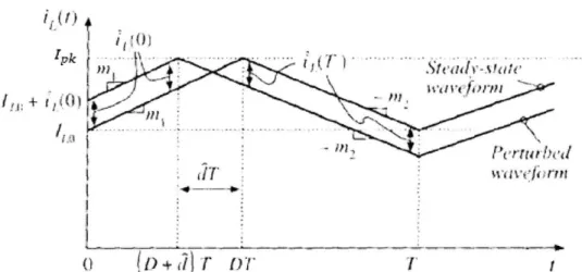
The converter will be unstable for duty cycles greater than 0.5 unless we
Consider the steady-state inductor current waveform in Figure 2-15. For the first part of the period, the inductor current increases with slope m, until it is equal to the peak current value, Ipk. So we can calculate Ipk as
I pk i (dT )= (0)+ m=dT (2.32)
Ipk -..-....
0 dT T
Figure 2-15. Steady-state inductor current.
Solving (2.32) for d gives us
d= I (O) (2.33)
m1T
During the second part of the period, the inductor current decreases with slope -m 2. We
can calculate the current at the end of the period as
(2.34)
= iL
(0)+
midT - m2d'TIn steady-state operation, the following relations hold
iL (0)= iL
(T)
d =D mi =M 1 m2 = M
2
Substituting these relations in (2.34) yields
O=MIDT-M 2D'T , (2.35)
which can be rearranged as
M2 - D
MI D' (2.36)
Assume there is a small perturbation,
It
(0), in the inductor current. Figure 2-16 shows the inductor current waveforms in the case of steady-state and for a slightperturbation. The slopes of the waveforms are approximately the same. From Figure 2-16, we see that
It(0)
can be expressed asIL (0) = -mT (. S t c .... ). (A: +I~ 10 'II 0 f()+JZT D1 T I
Figure 2-16. Inductor current in steady-state and with a slight perturbation.
Similarly, the perturbation from equilibrium at the end of the period can be expressed as
IL(T
2dT (2.38)Combining (2.37) and (2.38) results in
iL(T)= (0 f( (2.39a)
Or equivalently,
We can calculate the perturbation at the end of the next period and so on. The perturbation after n periods is
(2.40)
As n goes to infinity, the perturbation goes to zero if
D <
- <1
1- D
or equivalently,
D <0.5.
Otherwise, the perturbation increases without bound. This demonstrates that the converter is unstable for duty cycles greater than 0.5.
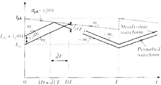
We can introduce a current ramp of slope ma and sum it with the current sense waveform at the input of the PWM comparator. This causes the inductor current to ramp up during the first part of the period until the sum of the current ramp, ia, and the inductor current reach the peak current, Ipk. This can be expressed mathematically as
iL (dT)+a (dT) = Ipk (2.41)
I
L _ D "nor equivalently,
(2.42)
This is shown graphically in Figure 2-17.
I
(Tpk 0rpk ~~
Figure 2-17. Inductor current in steady-state with slope compensation ramp.
Again, assume there is some perturbation,
IL
(0), in the inductor current. Using the same approach as before, we can see from Figure 2-18 that the perturbation at the beginning of the period can be expressed asIL
(0) = -dT(m
1 + m,) (2.43)lpk
) i + T
4 ~vrb~.;'
* ~-*
W I. I
Figure 2-18. Steady-state and perturbed inductor current with slope compensation ramp.
and that at the end of the period as
SL(T)= -dT(ma - M2)
Combining (2.43) and (2.44) results in
I':'
(T )=I (0 -M2 - M"aAfter n periods, the perturbation becomes
I
L (nT=mL( 2 ma mi + ma 2.44) .45) 2.46) TAs we can see from (2.46), the condition that must be satisfied to ensure that the perturbation goes to zero and the system is stable is
- m a <1 (2.47)
Mi+ ma
Thus, for sufficiently large compensating ramp slope, ma, the system will be stable for arbitrarily large D.
2.3 PWM Controller Using Commercial Integrated Circuits
The objective is to design our own PWM control chip transistor by transistor. We will first put together a control circuit using commercial operational amplifiers,
comparators, and other ICs to help develop an understanding of how the circuit and each functional block operates. Then we will use transistors to design a circuit to replace each block. An existing current mode pulse width modulation control chip, Unitrode's
UC3842, was used as a starting point and guide for the initial circuit design. See Figure 2-19 for a functional schematic of the UC3842. For additional information regarding the features and capabilities of the UC3842, refer to [4]. After reviewing the operation of this and similar control chips, we can determine some of the basic requirements for our PWM controller.
Vcc72 334V UVLO GROUND 5 9 C E VREF 2.50V5.0V CRN C A0MAINTERNALO VREF BIAS GOOD71 LOGIC Vr, RT /CT- C ERROR OUTPUT AMP 2R
VF8R LyR ATCH POWER
COMP CURRENT GROUND
SENSE
CURREN COMPARATOR
Note 1: A/B A= DIL-8 Pin Number. B = SO-14 and CFP-14 Pin Number. Note 2: Toggle flip flop used only in 1844 and 1845.
Figure 2-19. Functional Schematic of Unitrode's UC3842.
We need an internal voltage reference to which feedback from the converter's output can be compared to determine if the converter is being regulated properly. There must be an error amplifier to compute the error between the converter's output and the reference voltage and to provide some compensation to ensure that the loop is stable. For peak current mode control, we need an amplifier to sense and amplify the voltage across a current sense resistor placed in series with the high-side switch. A comparator is required to compare the current sense output to the level set by the error amplifier and signal when the current is too high. The converter and controller alternate between two states. In the first state, the high-side switch is on, the low-side switch is off, and the inductor current is ramping up. In the second state, the high side switch is off, the
low-side switch is on, and the inductor current is ramping down. We need an RS latch to keep track of which state the system is in. The second state is triggered by a pulse from the PWM comparator indicating that the current has exceeded the threshold. An oscillator
circuit is needed to produce a pulse at the desired switching frequency. This pulse is used to initiate the first state. We must have delay circuitry to prevent shoot-through and a gate drive circuit is required to convert the 0-5V logic signal into a larger magnitude signal and source enough current to charge the capacitance associated with the
MOSFETs' gates. Additionally, in order to operate the converter at duty cycles greater than 50%, we must provide some slope compensation to ensure stability. The remainder of this section briefly presents each block and an IC implementation of it. More detailed explanations of the blocks are given in Section 4.
We will assume a 12V supply is available to power our control circuitry. The circuit uses some logic ICs which require a 5V supply. This can be obtained from a linear voltage regulator, such as an LM7805. The desired output voltage for our
converter is 5V. We can either directly use the 5V supply as a reference or we can use an op amp to create a 2.5V reference from the 5V supply. Figure 2-20 shows an LM7805 used to create a 5V supply and a possible op amp configuration for generating a 2.5V reference. + 12v U LM78G5 In Out 5V JC i COrn C R
There are several options for the clock, or oscillator, circuit. We could use an LM555 timer, a 74LS123 or other one-shot chip, a Schmitt inverter, or one of numerous other options. Let's use a relaxation oscillator constructed with an LM311 comparator in a positive feedback configuration. The voltage across the capacitor will be used to generate our slope compensation ramp. The complete operation of the clock circuit is discussed in Section 4.4. See Figure 2-21 for a schematic.
C R2
+vR3 Camp. (Clock
Pulsa-R4 R5
Figure 2-21. Relaxation oscillator used to generate clock pulse and slope compensation ramp.
An RS latch can be implemented with NOR gates, such as those contained in the 74LS02 chip. Having the outputs of a pair of NOR gates each tied to one input of the other creates a latching effect. Applying a high voltage to the other input of one of the NOR gates sets the outputs of the NOR gates such that one is high and the other is low. The high input voltage can then be removed, and the gate outputs will remain the same until the state of the latch is changed by the application of a high voltage to the other NOR gate's input. RS latch operation is explained more in Section 4.7. See Figure 2-22 for a schematic.
R2 14 PWM 2 U Comparator 3 74LS02 1 0 7 5U 4 Clock 6 74LS2 S
Figure 2-22. RS latch implemented with NOR gates.
For the current sense amplifier, we need a high speed op amp to amplify the voltage drop across the current sense resistor. General op-amps, such as the LM741 or LF356, are not fast enough for this application. Texas Instruments' TLC070 was found to be an appropriate selection. The op amp used for the current sense amplifier operates with a 12V supply. However, the inputs to the amplifier are approximately equal to the input voltage to the converter, which can be as high as 20V. With input voltages so high, transistors within the op amp become saturated and the amplifier no longer functions properly. The average of the two inputs to the op amp is called the common-mode input. The difference between the two inputs, which is what we'd like to amplify, is called the differential-mode input. We refer to the range of common-mode inputs over which the op amp functions properly (i.e. no transistors are saturated) as the common-mode range. This maximum common-mode input is typically a bit lower than the supply voltage. So we must reduce the maximum common-mode input from 20V to something below 12V. This can be accomplished with a resistive voltage divider. We must use high precision, well-matched resistors because any mismatch will affect the output of the amplifier and result in our circuit having poor common-mode rejection. See Figure 23 and Figure 2-24 for output waveforms from the current sense amplifier operating normally and when
its common-mode input range has been exceeded. Figure 2-25 contains the schematic of our current sense amplifier, a TLC070 configured as a differencing amplifier with a gain of 39.
4-14.00Mis' A; CM Jr siomA
Ch4 1O0MAO
Figure 2-23. Inductor current and current sense waveform.
. . ...T -I- - -... I . . .-T. C4 10-0mAC *
Vs
K
Mi O.0jis A Ch4 r slOmA|Figure 2-24. Inductor current and current sense waveform when common-mode input is too high. a *fj2. 00 V B E Mf 2.00 N __ * 1 - --- ... .... F A 1. . ... . .. . . . .... ... ..
3911k R 1k R + /\/%v Viti TLC07 k 11 7 k \A---Top FET I' s R Dr-ain 39k
Figure 2-25. Current sense implemented with an op amp configured as a differencing amplifier with gain of about 39.
The delay can be an open-loop delay of a specified amount of time generated by a circuit such as the one shown in Figure 2-26. In this circuit, the delay is set by the time constant of the resistor and capacitor. Alternatively, we can implement a circuit that senses the gate to source voltage of one of the FETs and doesn't allow the other FET to be switched on until that voltage is below some threshold. This is a much safer
implementation and makes it much more difficult for shoot-through to occur. An example circuit is contained in Figure 2-27.
D
V,
11 10 R 13 12 DELAY
V6 deV-
+ 12v 5 Low Vgate + bd 2 s a _5of to te 3 74LS02 Hdgh I river 4 ram Latch 1 1 7 74HC1 7 +12v +5V High VgatFe> +5 R
6From Latch 6lLw deDir
Figure 2-27. Shoot-through is prevented by making sure a FET is sufficiently off before the other
FET is switched on.
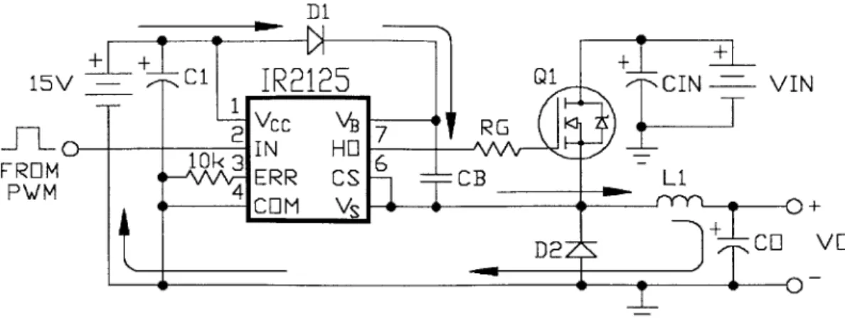
We need a circuit to turn the MOSFETs on and off as instructed by the signals from the delay circuit. This can be accomplished with a gate driver, such as an IR2125.
Figure 2-28 shows the typical connection of an IR2125 driving a low-side FET. Figure
2-29 shows an IR2125 configured to drive the high-side FET of a buck converter.
Figure 2-28. IR2125 gate driver used to drive low-side MOSFET.
Up 500V
Vc
Vc VBIN<>-- IN HO
ERR CS
D1
---
C.IR2125
3VCC VB - -- IN HO 3 ERR CS -CoM VS ±T +1 Di CIN - VIN R G CB Li + D2 +CO a 12Figure 2-29. IR2125 gate driver used to drive high-side MOSFET.
The error amplifier is just a typical op-amp, such as an LF356, configured as shown in Figure 2-14 and the PWM comparator is implemented with an LM31 1. See the full control schematic in Figure 2-30.
Cb k Rs O sc. Rasp IIAA 39k R lk R TLCO Rsm Slope Compensation W9 : E
R U~~~.5 Current SonseQim 3F i
PWM1 Comparator
+ 74L
Error Amplifier
Clock9 ?4LS02
R R4 a Dela Circite (o high side driver[
+ 2.5V D, t o to. side drivWr
35 .1 ( ki
+5V
Figure 2-30. PWM peak current mode control circuit for a buck converter.
15V F- t FROM PVIM 0 H.S
3 Analog Circuit Blocks
3.1 Current Sources
The collector current of a bipolar junction transistor can be described by (3.1).
ic =IseVj(+YA j (3.1)
The constant, Is, depends on the physical device characteristics of the transistor.
Collector current, ic, increases exponentially with base-emitter voltage, vBE. This means
that a very slight change in vBE causes a much larger change in ic. It turns out that vBE is
approximately 0.6V over a wide range of typical collector currents. The collector current also depends on collector to emitter voltage, VCE, through its ratio to the Early voltage,
VA. The Early voltage is generally much larger than vCE, so we can assume that term will be negligible and ignore it in our calculations. The denominator of the exponent in (3.1) contains the thermal voltage, VT. The thermal voltage is defined in (3.2) where k is Boltzmann's constant, q is the magnitude of an electron's charge, and T is temperature in kelvins. The value of VT is about 26mV at room temperature.
VT = (3.2)
q
In addition to the relation in (3.1), collector current is also related to the base current, iB,
as indicated in (3.3). The current gain, P, is a very large constant that depends on the transistor's device parameters, and is typically on the order of 100, making collector current much larger than the base current. For an npn transistor, the current flowing out of the emitter is the sum of the currents flowing into the collector and base. Because
P
islarge, we can neglect base current and assume that the emitter current is approximately equal to the collector current.
iC -- J8 "B (3.3)
Current sources are a fundamental building block for analog circuits. They are used to ensure that transistors are biased into the correct region of operation and often they determine the amount of gain an amplifier has. An example of a single-transistor
current source is given in Figure 3-1. The voltage at the base of the transistor is set by a voltage divider consisting of R1 and R2. The voltage at the emitter is vBE, or about 0.6V,
below that of the base, so the voltage across R3 can be controlled by setting the voltage at
the base. The voltage across R3 then determines the current through R3. The current through R3 is approximately the same as
Q's collector current which is the output of the
current source. This current source requires a number of resistors whose values can potentially be fairly large. In an IC implementation, resistance is proportional to area so a current source like the one in Figure 3-1 would typically not be used. It is reasonable, however, for a discrete implementation where large resistors are readily available, particularly because it requires only one transistor.
YCC
Rt I
M1
R2 BE R
3
Figure 3-1. Single transistor current source.
A common way of creating a current source on ICs is a circuit called a current mirror. Some reference current, Iref, is mirrored from a transistor to one or more other transistors, resulting in the current through those transistors being approximately equal to, or some scaled factor of, the reference current. A simple current mirror is shown in Figure 3-2. The reference current flows into the diode connected (meaning base and collector tied together) transistor Q1. Some of the reference current, iA, does not contribute to the collector current of Q1, but instead provides current to the two bases.
4I
re
ft
iA
Qi Q2
Since
P
is very large, this current is only a small fraction of the collector current. Thus, we will assume that the base currents are negligible and Iref flows entirely into the collector of Q1. Assuming that Q, and Q2 are well matched, the current, lo, flowing through Q2 is approximately equal to the reference current flowing through Q, because their base-emitter voltages are the same. Additional transistors may be added with their bases and emitters also connected to those of Q, and Q2 and the reference will be mirrored to them as well. As the number of transistors increases, however, the base current being drawn from Iref increases and is no longer negligible. In this case, the collector current of Q, can no longer be approximated as Iref. The current, iA, being drawn by the bases must be calculated and subtracted from Iref to determine the collector current of Q, that is being mirrored to the other transistors. The voltage at the collector-base terminal of Q1 is about 0.6V. One way of generating the reference current is to connect a resistor from there to a voltage source, as shown in Figure 3-3. The current Iref is then defined by (3.4).r VC -0. 6V(34
I = (3.4)
Vcc
R
tELo
Q 1 Q2
Figure 3-3. Simple current mirror with reference current set by the voltage across R.
The current mirror in Figure 3-2 is only accurate for well matched transistors. Any slight mismatch between the transistors means that they will have different values of Is so applying (3.1) we see that their collector currents will not be identical even though they have the same vBE. Additionally, collector current has significant temperature dependence. The variables IS, vBE, and vT all vary with temperature. So unless the transistors are at the same temperature, which is difficult to ensure with discrete components in separate packages, the collector currents will differ. In some cases, temperature mismatches can lead to a thermal runaway situation. The current flowing through a transistor causes its temperature to increase. The increase in temperature leads to a further increase in current which causes temperature to increase even more. The matching and thermal stability issues can be addressed by adding resistors to the emitters as shown in Figure 3-4. The emitter resistors provide negative feedback which provides
some stability to counteract thermal runaway. When the collector current of Q2
increases, the current through R2 goes up as well. This means the voltage drop across R2, and thus the voltage at the emitter of Q2, also increases. The voltage at the bases of the transistors is held constant because the collector current of Q, (and as a result, its vBE) is
unchanged. So the increase in the emitter voltage of Q2 results in a decrease in VBE2 which causes Ic2 to decrease. Thus R2 is providing negative feedback which counteracts an increase in Ic2. Doing KVL around the emitter resistor and vBE loop of the circuit
yields
VRl + VBEI = VBE2 + VR2
-Substituting the results of applying Ohm's law and solving (3.1) for vBE we get
ic1R +VT In icj =VT In ic2 +ic 2R2
-Isi Is2
Solving for iC2R2 yields
iC2R2 =Ci1RA +VT ln ic1j -VT In ic2
(Is2)
We can combine the two natural log terms to obtain
iC2R2 = iciR +Vr n .S2
+V Isi 1C2
Dividing both sides by R2 gives us the output of the current mirror
iC2 = ici -1+ Vr-I i i - .
R2 R2 (Is1 iC2
Assuming Qi and Q2 are matched, Isi = IS2 and (3.5a) reduces to
iC2 = ici + VIn . R2 R2 Kc2J
(3.5a)
Q1 02
R2
Figure 3-4. Current mirror with emitter resistors to improve accuracy and temperature stability.
The equation in (3.5a) shows that if there are not extreme differences between the Is and Ic values of the two transistors and if the voltage drops across the emitter resistors are much larger than VT, the natural log term is negligible and (3.5a) can be simplified to
iC2 = jci -Ri .(3.6) R2
So, by adding emitter resistors and ensuring that the voltage drop across them is much larger than 26mV, we've gained stability against thermal runaway and the relationship between the output current and the reference current now depends primarily on the ratio of R1 to R2, regardless of how well matched the transistors are. Setting R1=R2 mirrors the
reference current to the output, but we also have the additional flexibility of choosing R1
not equal to R2 and having an output current different from the reference current by some
In the current source circuits we've discussed thus far, the goal was to generate a constant current of some value that had little variation with changes in transistor device parameters or temperature. There are some situations in which we actually want a current that increases predictably with temperature. These are known as proportional-to-absolute-temperature (PTAT) current sources. Consider the circuit in Figure 3-5.
Applying KVL to the lower loop yields
VBE1 V BE2 + VR VBE2 + iC 2 R
which implies that
AvBE BEI BE2 C2R
Solving (3.1) for vBE and substituting yields
VT In kJ - VT ln j = iC2R.
We can combine the two natural log terms to obtain
VT In -kLh =iC2R
ISi C2
Substituting (3.2) for VT yields
kT In ic 'S2 =iC2R.
q )Is1 iC2
The output current is then expressed as
C2 = 1 -(U).In .
f
j.
(3.7)C2R q Is1 _iC2
This derivation shows that the voltage across (and current through) R is directly proportional to temperature, assuming that the natural log term can be held relatively constant. Because
P
is large, iC2 is approximately equal to the current through R and so is also PTAT. In general, the difference between two base-emitter voltages is PTAT.Ire ~
IPTAT
01 02
R
Figure 3-5. Basic PTAT current generator.
Figure 3-6 contains an implementation of a PTAT current source. The current mirror formed by
Q3
andQ4
keeps the collector currents ofQ,
and Q2 the same. So Ic, and IC2 cancel each other in the natural log term of (3.7). By connecting two transistors in parallel to serve as Q2, we have doubled the area of Q2 which means that Is2 is now twice as large as Isi (assuming the three transistors are well matched) so (3.7) simplifies to1C2 ~1. -Iln(2).
So iC2 and ici are PTAT, as desired. Connecting these two transistors in parallel is analogous to how transistor areas are scaled in an integrated circuit. In order to extract this PTAT current,
Q5
is connected as shown in Figure 3-6 so that the current is mirrored there as well. The collector current ofQ5
is our PTAT output current. This current can now be applied directly to a circuit or it can be converted to a PTAT voltage via a resistor. The output current is determined by the ratio of Qi and Q2's areas. By varying R and the number of transistors connected in parallel to form Qi or Q2, we can control the value of IPTAT.Vcc
03 Q4 Q5
Q1 Q2
R
Figure 3-6. Implementation of a PTAT current source.
3.2 Common Emitter Amplifier
Figure 3-7. The input signal is applied across the base-emitter junction and the output is taken from the collector. We replace the transistor with its small signal model to
determine the characteristics of the circuit. An equivalent circuit for analysis is shown in Figure 3-8. For a derivation of the small-signal model for a bipolar junction transistor, refer to [5].
VCC RL
Vout
V.n
Figure 3-7. Common emitter amplifier schematic.
-~n 1 9 x r 0~ RL Vout
Figure 3-8. Small signal model for common emitter amplifier.
Assume a small signal input, vin, is applied as shown. The input shows up across
r,, thus vn=vin. The value of the dependent current source is then gmvin. By applying
r0 and RL. Assuming r, is much larger than RL, r0 can be neglected. Thus the output
voltage is
Vo,= -,,vi, -(RL lro)
-m in -RL
The gain of the circuit is then
a = 'vout ~ -gm - RL in
Input resistance is the resistance seen looking into the input terminal of the amplifier. It is the resistance seen by the output of some previous stage or some input source that may drive this circuit. The input resistance is defined as
(3.8)
(3.9) Ri = in
iin
For the CE amplifier, Rin=r,. Analogous to input resistance, output resistance is the resistance seen looking into the circuit from the output terminal. The formal definition is
(3.10) Ro = out
In this case, setting vin to 0 turns off the dependent current source, making it an open circuit. The resistance seen from the output is then the parallel combination of r0 and the
load resistance, RL. For cases where RL is much smaller than r0, Rout is simply
RL-3.3 Emitter Follower Buffer
Another useful analog block is the common collector (CC) or emitter follower (EF) configuration. This circuit, depicted in Figure 3-9, consists of a single transistor with an input voltage applied at the base and output taken at the emitter. The equivalent small signal circuit, shown in Figure 3-10, can be analyzed to determine the
characteristics of the EF.
VCC
V.M
- 7L Vout
+ + r V2r
+
out
Figure 3-10. Small signal model for emitter follower.
Applying KCL at the output node yields
OV
- v otv ot- OVii +RP in + " - ""' = 0
t'ORn (because gv, =lo6in ).
Substituting for iin results in
vin -vout + i -- voR,
r, r,
, = 0
r0 RL
Upon simplification we get
y out vin
1+
(ki
+1)(ro DIRL)Assuming 8 >>l and ro >> RL , we can use the relation r, = -4 to obtain
g,
(3.11a)
(3.1lb)
9M VA ro
The gain of the EF is less than 1. It turns out that, due to the transistor's factor of f current gain, any resistance connected to the emitter seems larger by a factor of P+1 when viewed from the base of the transistor. Likewise, when looking into the emitter, r" and any resistance connected to the base seem smaller by a factor of $+1. See [ ] for a derivation of this. Using this information, we can determine Ri, and Rut without too much hassle, as indicated by (3.12). Otherwise we would have to apply a test input source and analyze the circuit to determine the ratio of the input and output voltages and currents. in= r, +i(o +1)(r, JR) ~ r, + (,80 + 1)RL (3.12a) r Rou, = r RL fo +1 Because r, is very large,
Rout = RL r,,
'go +(3.12b)
Rout = RL 1
gM
When 80 >> 1, r, >> RL, and gRL >> 1, the gain of the emitter follower is
output resistance and increases the effective input resistance seen by adjacent stages by a factor of P+1 make the EF amplifier a good buffer to use before, between, and after other stages.
3.4 Differential Pair
We often need to take some differential voltage as input and amplify it. This can be done with the differential pair circuit block shown in Figure 3-11. Assume a
1 differential voltage, vd, is applied across the input terminals. We model this as + -vd
2 1
applied to the base of Qi and - -vd applied to the base of Q2 as
2 indicated in Figure 3-11.
The change in collector current for a given change in vBE can be calculated as follows: Ignoring the Early effect, (3.1) becomes
VBE
ic =Ise V. (3.13)
We differentiate (3.13) with respect to vBE to obtain
____ 1 VBE
= - Ise VT
aVBE VT
This expression is equivalent to
ic _ c
avBE T
I,
- V (when evaluated at the DC operating point).
VT
ac = I = gM. (3.14)
avBE T
The change in collector current for a given change in VBE is known as the
transconductance and is typically associated with the variable gm. (3.14) can be used to determine what the change in ici and iC2 will be as a result of the applied differential
input voltage. The expression in (3.14) implies
Aic = g,- AvBE. (3.15)
So the change in icl will be gm* + IVd and the change in iC2 will be g,. -
Vd-These currents flow through the load resistors. To obtain a differential voltage output, we can take the difference between the voltages at the two collectors, indicated as vod in Figure 3-11. The change in voltage at the collectors in response to the change in ic is
- Aic -RL . So at the collector of
Q,
we getVol = -AiCl - L
Substituting for Aic yields
Vo1 = -g,. - RL (3.16a)
2 At the collector of Q2 we get
RL-Again, substituting for Aic yields
v02 =-g,n -R v,2 = , - - R ,
2 The differential output voltage in response to Vd is
Vod = V01 - V 2
Substituting the results from (3.16) yields
Vd
2
which can be simplified to
The gain of the differential amplifi
vod = -g-v -R er is (3.17) (3.18a) a, = = -gMv RL. Vd
If we were to define the differential output voltage as Vod = - v0 1 , the amplifier would
be non-inverting and the gain would be
av = vod= gm- RL Vd (3.18b) (3.16b) V _gM. ' -RL 2
Vcc RL RL .ci + Vdd -C 1 2Q190 +Yd/2 O'C 02 Y/ YIce
Figure 3-11. Differential pair amplifier schematic.
If, instead of a differential output voltage, we wanted a single-ended output voltage referenced to ground, we could take either v0 i or vo2 as our output. A single-ended output
is advantageous because it is referenced to ground, however the gain is reduced by a factor of 2. For instance, with voi taken to be the output
a = = , -RL. (3.19)
Vd 2
From the gain expressions derived above, we can see that the gain of the differential pair is proportional to the bias current (through gm) and the load resistance. Because power dissipation is proportional to current, it is not ideal to use large bias currents to increase the gain. Large resistors are impractical for integrated circuits because resistance is proportional to area and a primary objective in integrated designs is
to minimize size. The solution is to use transistors, instead of resistors, to load the differential pair. This configuration, known as an actively loaded differential pair, is shown in Figure 3-12. The small signal model for the bipolar junction transistor includes an output resistance, designated by ro. This is the resistance seen looking into the
collector of the transistor. The output resistance is proportional to the Early voltage, VA, and is typically very large.
r A (3.20)
IC
The effective resistance seen at the output node is
RLe = r.2 11 r.4
which becomes
_VAflVAP
IC2 IC4
Vcc 03 04 'CLI V0 C Ctj O iC2 Q1 02 '-Vd/2 -Vd/2
41
[ccFigure 3-12. Actively loaded differential pair amplifier.
Note that the early voltages for npn and pnp transistors are different. VA is typically significantly larger for npn transistors. The increased resistance seen at the output node significantly increases the amount of gain the circuit can provide. In the case of the resistively loaded differential pair, the effective load resistance seen at the collectors is actually RL in parallel with the transistor's r. However, because r0 is so much larger than
RL, we were able to ignore it in the previous calculations. The actively loaded
differential pair provides a significant increase in gain, but this circuit is only useful when a single-ended output is desired because we can only take the output from the collector of Q2 as opposed to in the resistively loaded case where we could take a differential output voltage.
Figure 3-13 contains a graph of the vw versus vd transfer characteristic for a differential pair amplifier. The circuit only amplifies linearly over a small range, about
± 25mV , of differential input voltages. Beyond this range, all of the bias current is
change the collector currents or output voltage. Emitter resistors can be added to the input transistors, illustrated in Figure 3-14, to widen the linear range of the amplifier. For a factor of m increase in linear range, set - RE ICC equal to mVT. Figure 3-15 shows the
2
1
vo versus Vd transfer characteristic for the case where -REICC is about 20V. Upon
2
examining the slope of the curve in Figure 3-15, we can see that the gain of the circuit is reduced by approximately the same factor by which the linear range is increased. The following calculations show that the gain is approximately the ratio of RL to RE if we take the output voltage differentially.
Increasing linear range by m
1
-RE CC T(3.21)
2
implies a reduction of the gain by a factor of m yielding
m
Substituting the results of (3.21) and the expression for gm gives us
i sVT .- R
which simplifies to -RE ICC T (.1
avRL vR E