Double-Sided Graphene Oxide Encapsulated
Silver Nanowire Transparent Electrode with
Improved Chemical and Electrical Stability
The MIT Faculty has made this article openly available.
Please share
how this access benefits you. Your story matters.
Citation
Chae, Woo Hyun, Thomas Sannicolo, and Jeffrey C. Grossman.
“Double-Sided Graphene Oxide Encapsulated Silver Nanowire
Transparent Electrode with Improved Chemical and Electrical
Stability.” ACS Applied Materials & Interfaces 12, 15 (April 15, 2020):
17909–20. © 2020 American Chemical Society
As Published
http://dx.doi.org/10.1021/acsami.0c03587
Publisher
American Chemical Society (ACS)
Version
Final published version
Citable link
https://hdl.handle.net/1721.1/125420
Terms of Use
Creative Commons Attribution 4.0 International license
Double-Sided Graphene Oxide Encapsulated Silver Nanowire
Transparent Electrode with Improved Chemical and Electrical
Stability
Woo Hyun Chae, Thomas Sannicolo, and Jeffrey C. Grossman
*
Cite This:ACS Appl. Mater. Interfaces 2020, 12, 17909−17920 Read Online
ACCESS
Metrics & More Article Recommendations*
sı Supporting InformationABSTRACT: Owing to their high conductivity, transparency, flexibility, and compatibility with solution processes, silver nanowire (AgNW) networks have been widely explored as a promising alternative to indium tin oxide (ITO). However, their susceptibility to corrosion and thermal instability still remain limiting factors for widespread adoption in a range of devices including solar cells, transparent heaters, and light-emitting diodes. In this study, we report a scalable and economically viable process involving electrophoretic deposition (EPD) to fabricate a highly stable hybrid transparent electrode with a sandwich-like structure, where a AgNW network is covered by graphene oxide (GO) films on both sides. The newly developed all solution process allows the conductive transparent film to be transferred to an arbitrary surface after deposition and demonstrates excellent sheet resistance (15Ω/sq)
and tunable transmittance (70−87% at 550 nm). Unlike bare AgNW networks, the hybrid electrode retains its original conductivity under long-term storage at up to 80% relative humidity. This chemical resilience is explained by the absence of silver corrosion products for the AgNW encapsulated by GO as indicated by X-ray photoelectron spectroscopy. In situ voltage ramping and resistance measurements up to 20 V indicate a novel stabilization mechanism enabled by the presence of GO which delays the failure onset and prevents abrupt divergence of the resistance to the megaohm range experienced by bare AgNW networks. The double-sided nature of the GO coating offers combined stability and performance to the AgNW network, which adds unique versatility of our electrodes to be used toward applications that require a wide range of thermal and chemical stabilities.
KEYWORDS: silver nanowire, percolating network, graphene oxide, electrophoretic deposition, stability
1. INTRODUCTION
Indium tin oxide (ITO) has been widely used as transparent electrodes1,2 in optoelectronic devices thanks to its superior optical transmittance (90% at 550 nm) and low sheet resistance (20Ω/sq).3However, the limited supply of indium, high cost of sputtering, and the brittle nature of ITO inhibit its widespread adoption to next-generation flexible and stretch-able electronics.4 Networks of solution synthesized metal nanowires (MNW)5,6such as those made of silver nanowires (AgNW) are promising as alternative transparent electrodes. AgNW networks are compatible with scalable deposition techniques, are mechanically robust, and demonstrate sheet resistances as low as 10Ω/sq and transparency (at 550 nm) between 80% and 90% without substrate, which meets the requirements for most target applications.7 Yet, despite the significant benefits, AgNW networks (and more broadly any MNW network) lack in chemical, thermal, and electrical stability, largely due to their high surface-to-volume ratio.8−10 For example, silver undergoes spontaneous sulfidation to form silver sulfide (Ag2S) particles by reacting with atmospheric
species such as carbonyl sulfide (OCS).8Also, MNWs undergo spheroidization by Rayleigh instability under high temperature induced by Joule heating. This causes the MNW network to lose its percolative nature over short time scales at high applied voltages or over longer times at low applied voltages.10,11Such instabilities are significant technological barriers to the widespread application of NW networks as reliable transparent electrodes.
By hybridizing MNWs with other materials, previous studies have demonstrated that it is possible to complement the drawbacks of each material by harnessing the advantages offered by another. Coating the nanowires with graphene
Received: February 24, 2020
Accepted: March 25, 2020
Published: April 1, 2020
Research Article
www.acsami.org
This is an open access article published under a Creative Commons Attribution (CC-BY)
License, which permits unrestricted use, distribution and reproduction in any medium, provided the author and source are cited.
prepared by chemical vapor deposition (CVD) has been explored as an effective strategy to preserve the nanowires’ optoelectronic properties while adding stability. However, the growth of large-area graphene by CVD is expensive, and research is still underway to enable mass production. Conformal transparent metal oxide coatings deposited on MNW surfaces were also realized by atomic layer deposition (ALD)12,13 which adds little cost benefit over processing conventional sputtered ITO. Although seminal efforts using atmospheric pressure spatial ALD were recently made to make these conformal coatings more scalable and low cost,14,15most of the aforementioned deposition techniques involve high temperature and high vacuum, losing all the benefits of fabricating AgNW networks by a solution-based process and causing incompatibility withflexible plastic substrates with low thermal budget.
Alternatively, integration of MNWs with inexpensive and solution-processable graphene oxide (GO) or reduced graphene oxide (rGO) was explored by using spin coating,16 dip coating,17 rod coating,18 and spray coating,19−23 but challenges still remain in terms of large-scale processing. For example, spin coating is a lab-scale batch process that also results in inhomogeneous films due to edge effects and the centrifugal force on particles. Moreover, the size of the substrate is severely limited, as with vacuum filtration. Spray coating incurs a risk of spray nozzle clogging or unsteady operation, which may be a concern for nanomaterials with high aspect ratios. This may require hours of sonication to break up the GO sheets or necessitate use of ultrasonic sprays which tend to break or damage micrometer-sized GO sheets,24,25 placing restrictions on the morphology of thefinal GO film. In addition to such drawbacks, a critical limitation for all of the conventional solution-based deposition techniques is that the choice of substrate is restricted to those with a planar geometry, and pretreating them to optimize the wetting properties is critical to mitigate inhomogeneities such as “coffee stains”.26
Furthermore, although previous studies have demonstrated an AgNW-GO hybrid structure, many aspects of the chemical and electrical stability of AgNW networks imparted by the presence of GO either have not been fully demonstrated or remain poorly understood.
In this work, we report a novel fabrication process that utilizes a scalable and economically viable electrophoretic deposition (EPD) method and GO solution dip treatment to fabricate highly stable transparent electrodes where the conductive AgNW network is effectively “sandwiched” between a seamless EPD-GOfilm with tunable thickness and ultrathin GO (Dip-GO) composed of 1−2 layers. We demonstrate that the GO layers enhance contact between NWs to reduce the junction resistance, mitigating the need for treating NWs at high temperature. Our films demonstrated excellent sheet resistance as low as 15 Ω/sq and a tunable transmittance of 70−87% by simply tuning the EPD parameters.
Furthermore, the increase in thefilm stability was shown to depend largely on which GO layer is protecting the underlying AgNW network. When Dip-GO is exposed to air (“Dip-GO up”), stability reinforcement of the electrode is observed, although partial degradation can still occur. However, when EPD-GO was exposed to air (“EPD-GO up”), our hybrid electrode retains its original conductivity under long-term storage at 80°C in both moderate (55% relative humidity) and high (80% relative humidity) humidity conditions. The
exceptional chemical stability offered by the EPD-GO layer was verified by the absence of major silver corrosion products for the AgNW as indicated by X-ray photoelectron spectros-copy (XPS). Finally, for the first time, an in situ voltage ramping test up to 20 V was performed on a GO-AgNW composite structure. The results indicate a novel stabilization behavior enabled by the presence of GO that prevents abrupt divergence of the resistance to the MΩ range experienced by bare AgNW networks.
Importantly, our process allows thefilm to be transferred to arbitrary surfaces with desired orientation such that either EPD-GO or Dip-GO is facing up. This freedom adds versatility for future device integration where certain properties need to be emphasized over others as they are strongly correlated to the thickness/robustness of the GO protecting layer being used. For instance, a thick EPD-GO layer offering increased chemical and electrical stability at elevated temperatures and high voltages could be preferentially used at the top when integrating thisfilm in a transparent heater, while an ultrathin Dip-GO layer could be preferentially used as an interfacial layer in solar cells as a way to enable Ohmic transport and optimize the energy level matching with other layers.
2. EXPERIMENTAL SECTION
2.1. Fabrication of Transferrable EPD-GO/AgNW/GO Film. Prior to EPD, two 2.54 cm × 2.54 cm 316 stainless steel plates (McMaster Carr) are cleaned thoroughly by ultrasonication in acetone, followed by rinsing in ethanol and deionized water. One of the plates to be used for EPD deposition is then spin-coated with cellulose acetate (Sigma-Aldrich) solution in acetone (4 mg/mL) with a spin speed of 900 rpm for 1 min. The steel plates are then attached parallel to each other in an electrophoretic deposition (EPD) cell with a fixed distance of 5 mm. The deposition substrate with cellulose acetate coating is attached to the positive contact as an anode. The electrodes are then immersed in a diluted aqueous GO solution (Graphenea), and a constant voltage of 5 V is applied across the EPD cell for 4 min by using a Tektronix PS-282 DC power supply, leaving a thinfilm of EPD-GO on the anode. The electrodes are then slowly withdrawn from the GO solution. The EPD-GO on a stainless steel plate is spin-coated with the AgNW solution in isopropanol (2 mg/ mL, ACS Materials) with a spin speed of 600 rpm for 40 s. The NW average diameter is 50 nm. The NW average length is in the range 100−200 μm. The resulting AgNW-based product on a stainless steel plate is then immersed in 1.5 mg/mL aqueous GO solution for 1 min before being rinsed by deionized water and blow-dried with nitrogen gas. Next, the entirefilm on the stainless steel plate is immersed in acetone for at least 6 h and then transferred to deionized water. The transparent EPD-GO/AgNW/GO film is then liberated from the underlying steel substrate and is transferred to a transparent insulating substrate such as glass (Corning Eagle XG) or PET (DuPont Teijin Melinex ST505). Finally, the transferredfilm is dried on a hot plate at 40°C and thoroughly rinsed with acetone and ethanol.
2.2. Optical, Electrical, Chemical, and Morphological Characterization. The optical characterization of electrodes was performed with a PerkinElmer Lambda 1050 UV−visible−near-IR spectrophotometer equipped with an integrating sphere. A Jandel cylindrical linear four-point probe with a tungsten probe separated by 1 mm with a probe radius of 40μm was used to measure the sheet resistance of all the electrodes. Sheet resistance measurements were taken on five different spots for each sample and averaged. X-ray photoemission spectroscopy (XPS) measurements were performed on a Thermo Fisher Scientific K-Alpha system with a monochromatic Al Kα X-ray source (1486.6 eV). Surface charging effects due to the insulating nature of GO were compensated for by using a low-energy flood gun. Step sizes of 1 and 0.1 eV were used for survey scan and high-resolution spectra, respectively. Quantification and deconvolu-tion of spectra were performed by using the data analysis software
Avantage (associated with the K-Alpha system), after Shirley background correction. Scanning electron microscopy (SEM) images were obtained by using a Hitachi SU8100 high-resolution SEM with an accelerating voltage of 1−4 keV and a combination of upper (in-lens) and lower secondary electron detectors. Atomic force microscopy (AFM) measurements were performed on an Asylum Research Cypher AFM on standard AC-air tapping mode.
2.3. Chemical and Electrical Stability Studies. To perform chemical stability studies, the electrodes were stored on a Torrey Pines HP60A programmable hot plate set at 80°C either in the lab environment or inside a controlled humidity chamber (5533 environmental chamber by Electro-Tech Systems Inc.) and were only taken out once a day briefly to measure the sheet resistance. Relative humidity was recorded for the duration of the experiment with a VWR hygrometer. In situ electrical stability studies were performed with a Keithley 2401 sourcemeter unit (SMU) using two probes. Electrical contacts were made on opposite ends of 2.54 cm× 2.54 cm samples with a conductive silver paste (DuPont) and dried for 12 h in air. Voltage ramps were applied on the samples via a LabView program interfaced with the SMU. A FLIR A615 Infrared camera was used to record the temperature of our samples during voltage ramps.
3. RESULTS AND DISCUSSION
3.1. Fabrication Process and Structural Character-ization. We have developed a novel and cost-effective fabrication process utilizing electrophoretic deposition (EPD) and solution dip-treatment to create an EPD-GO/AgNW/GO hybrid composite transparent conductor. The process is illustrated inFigure 1a: (i) coating of a dissolvable sacrificial cellulose acetate (CA) layer on stainless steel (SS) substrate, (ii) EPD of GO thin film, (iii) AgNW coating, (iv) dip treatment in GO solution, (v) acetone bath to dissolve CA layer, and (vi) transfer onto arbitrary surface.
EPD is a colloidal deposition technique where an electric field is created within a colloid dispersion by applying a constant voltage between two electrodes immersed in the solution (Figure 1b). This attracts and deposits the charged colloidal particles to the electrode with opposite charge to form a dense film. As GO flakes dispersed in water are negatively charged due to the abundant deprotonated carboxylate groups, deposits will be formed on the positively biased anode upon EPD.27The advantages of EPD over other
solution-based processes include low cost, rapidity, simple equipment, controllable deposition rate, uniformity of deposition, and the possibility to be performed on surfaces with complex morphologies.28 In conventional EPD, as the deposition substrate is the electrode, it is difficult to detach the depositedfilm from the SS substrate (electrode). Therefore, to allow transfer of thefilm from the substrate, a sacrificial layer made of cellulose acetate (CA) was coated on the SS substrate prior to EPD to liberate the deposited structure upon immersing in acetone,27,29allowing transfer of thefinal EPD-GO/AgNW/GOfilm to arbitrary surfaces.
Upon deposition of thefirst GO layer by EPD (EPD-GO) on SS substrate to form EPD-GO/SS, AgNW was coated on top of the EPD-GO/SS by spin coating. The density of the AgNW is primarily responsible for the conductivity of thefilm and can be tuned by changing the concentration of AgNW solution and spin speed. It should be noted that the method of AgNW deposition can vary, and the inherent wettability of the GO allows AgNW to be easily coated by spray coating as well
(Supporting Information, Figure S1). Therefore, our process
has theflexibility to accommodate a variety of existing MNW coating techniques.
The resulting AgNW/EPD-GO/CA/SS structure is then simply dipped in the GO dispersion, rinsed in water, and blow-dried. This dip-treatment covers the exposed AgNW with ultrathin GOflakes to mechanically weld or fix the AgNW onto the EPD-GO layer and to create a sandwiched structure of GO/AgNW/EPD-GO/CA/SS. As has been proposed by Pei et al., electrostatic attraction between AgNW and GO flakes in solution causes the AgNW network to be covered in an ultrathin GO coating composed of only a few layers.30Coating the AgNW by ultrathin GO at this stage of the process is also beneficial to affix the AgNW network onto EPD-GO. The contact between AgNW and EPD-GO prior to dip treatment was indeed observed to be poor as evidenced by delamination of the AgNW thinfilm at the air−water interface (Figure S2). Note that performing the second GO deposition by EPD instead of dip treatment is prevented since AgNWs already present on the deposition substrate (positive electrode) would simply dissolve as a result of the applied positive bias. The subsequent acetone bath detaches the EPD-GO/AgNW/GO Figure 1.(a) Processflow for the fabrication of EPD-GO/AgNW/GO conductive films. (b) Schematic of the electrophoretic deposition (EPD) setup.
film by dissolving the CA layer and allows transfer to arbitrary surfaces. As illustrated at the end of the process schematic of
Figure 1a, transfer of thefinal conductive composite film can
be accomplished in two different orientations, where either the EPD-GO layer or the Dip-GO layer is facing up with respect to the target substrate.
3.2. Structural Characterization. Our fabrication process utilizing both EPD and solution dip treatment is not only scalable and cost-effective compared to existing techniques but also beneficial as it results in a novel composite structure where the AgNW network is “sandwiched” by two GO layers synthesized by two different means. The EPD-GO and Dip-GO that cover the AgNW network offer different properties to the final composite structure because of their structural differences which were characterized by SEM.Figures 2a and 2b show, respectively, the top and tilted view of the EPD-GO/ AgNW/GO film, where EPD-GO is facing up, and illustrate the EPD-GOfilm following the topography of the underlying AgNW network. It is notable that thanks to the capability of EPD to form continuous films over macroscopic areas, EPD-GO did not show any discontinuities such as gaps or holes that would expose the underlying AgNWs to the external environment.Figures 2c and 2d are analogous images where Dip-GO is facing up. Contrary to EPD-GO, it was difficult to conclude that GO was seamlessly covering the NWs for the Dip-GO side. In most areas, the AgNW network appears to be seamlessly covered with GO based on the little contrast difference of the NWs.Figure 2c, which is the top-down SEM view of the Dip-GO treated side of the film, clearly shows individual AgNW surfaces even at a low acceleration voltage of 1 kV due to the ultrathin nature of GO. The contrast was observed to be uniform on the NWs, indicating GOflakes are completely covering the NWs in view. However, nanoscale gaps between GOflakes exposing bare AgNW were detected
from the tilted view of another region of the same sample
(Figure 2d), as indicated by the arrows. The presence of such
nanoscale gaps and the contrast between individual Dip-GO sheets were more easily visualized by performing a dip treatment on AgNW networks on glass without underlying EPD-GO, as shown in the SEM images (in-lens detector) in
Figure S3a,b. This may be due to the stochastic nature of the
dip treatment as well as size differences (Figure S3c) between GO flakes and has implications for the AgNWs’ chemical stability as will be discussed subsequently. Finally, an SEM cross-section image (Figure 2e) of the EPD-GO/AgNW/GO film clearly reveals the morphology of our film where NWs are covered by a thicker EPD-GO on one side and an ultrathin GO layer on the other side, demonstrating the effectiveness of our simple and solution-compatible process in creating a GO/ AgNW/GO structure.
Utilizing EPD in the fabrication process allows the thickness of the GO to be easily controlled by simply tuning the deposition parameters. Among such parameters, the GO solution concentration was varied, while the deposition voltage and time werefixed in all experiments. Previous studies on the EPD of GOfilms31have demonstrated that the deposited mass is a linear function of the GO solution concentration, in line with the well-known Hamaker’s law for EPD.32The thickness of EPD-GO films characterized by atomic force microscopy (AFM) is plotted as a function of GO concentration inFigure 2f, revealing that the relationship between the thickness and GO solution concentration is close to linear. The detailed AFM images and height profiles of each EPD-GO film are shown in Figure S4. Although thickness of electrodeposited films has sometimes been reported to be inhomogeneous, particularly at the edges due to higher electricfield strength at the deposition substrate edges,33ourfilms exhibited very high thickness uniformity except at the sample edges (Figure S5a). Figure 2.SEM images showing EPD-GO/AgNW/GOfilm in various perspectives including (a, c) top-down view, (b, d) tilted view, and (e) cross-section view. (f) EPD-GOfilm thickness and total transmittance (at 550 nm) as a function of GO solution concentration.
As can be seen inFigure S5a, the representative thickness of the EPD-GO film in this case was the value at the center, corresponding to 19.5 nm. Starting from the film edge, the thickness decreases quickly to within 10% of the center thickness from a distance of about 3 mm from the edge. This suggests that on a 25.4 mm square sample the EPD-GO thickness is perfectly uniform over a length of 19 mm, meaning that 75% over the 25.4 mm length across thefilm has uniform thickness. This value matches well with the region of uniform electric field intensity simulated by COMSOL for the same sample size, which was about 76% of the sample length (Figure S5b). This region of uniform field should correspond to consistent EPD-GO thickness, as EPD deposition thickness depends on the electric field intensity.32 Furthermore, our simulations show that scaling up the substrate size increases the proportion of region with uniform field, which suggests that edge inhomogeneity does not prevent EPD from being a scalable process (Figure S5b). While other strategies to mitigate the edge effect by employing different sizes for the deposition and counter electrode during EPD have already been investigated,34 this is out of the scope of the present contribution.
Implementation of EPD in our process allows facile tuning of the GO thickness from roughly 15 to 100 nm. This in turn enables the optical transmittance (at 550 nm) to be easily tuned across a wide range from 75% to above 90% (Figure 2f), compatible with various optoelectronic technologies using transparent conducting layers.7 With longer deposition times and higher GO concentration, even thicker (micrometers thick) GOfilms can be easily realized through EPD.28Films with thicker GO-AgNW hybrid structures could potentially find applications in conductive membranes for electrochemical devices35,36or electromagnetic interference (EMI) shielding.37 3.3. Optoelectronic Characterization. The mean sheet resistance and total transmittance at 550 nm are the most important optoelectronic performance metrics for transparent conductors in general.2 However, for MNW networks,
electrical uniformity as well as light scattering deserves equally serious attention.38,39 In particular, ensuring low sheet resistance uniformly throughout AgNW networks is challeng-ing due to the high resistances between individual AgNWs at the junctions and potential lack of uniformity in the AgNW coverage itself as opposed to conductive metal oxides with continuous film morphology. To assess the magnitude and homogeneity of ourfilms, we have used the linear four-point probe (4PP) technique to measure the sheet resistance of our samples atfive different locations. Although GO is an insulator, the 4PP measurements were possible for sufficiently thin GO thicknesses below 25 nm, which was achieved for EPD-GO fabricated with 0.08 and 0.15 mg/mL GO solution.Figure 3a shows the mean sheet resistances of the samples with various configurations along with the standard deviations over the five values measured in each case. As-coated bare AgNW networks exhibited a mean sheet resistance of 40 Ω/sq with a large standard variation of 12Ω/sq, indicating that the resistances between wires are not only high but are also widely varying. In contrast, bare AgNW annealed at 200°C for 50 min showed a sharp reduction of sheet resistance to 13.6Ω/sq and a reduced standard deviation of 3.3Ω/sq, indicating that the majority of NW junctions have sintered to form more low-resistance conduction pathways.9 Our EPD-GO/AgNW/GO films demonstrated similarly low and homogeneous mean sheet resistance values. For both the EPD-GO side (0.08 mg/mL GO) and the Dip-GO side, mean sheet resistance values were 16 and 14.5Ω/sq, with standard deviations of 2.5 and 1.4 Ω/ sq, respectively. As a consequence, electrical optimization was achieved without resorting to any thermal treatment. Note that the slight difference in the sheet resistance values associated with the sample with EPD-GO up and the one with Dip-GO up is due to slight fluctuations of the density of deposited AgNWs by spin coating, which is inherent for any percolating structures. The electrical performance is only driven by the density of AgNWs.
Figure 3.(a) Sheet resistance of EPD-GO/AgNW/GOfilms compared with bare as-coated or thermally annealed AgNW networks. (b) Histogram showing height distribution of two nanowire junctions. AFM images of (c) bare AgNW network and (d) EPD-GO/AgNW/GOfilm. (e, f) AFM height profile of the same.
To further investigate the origin of the observed electrical optimization induced by the GO“sandwich” structure, we have performed AFM to characterize the NW junctions. Junctions where two NWs crossed were identified in the AFM images of EPD-GO/AgNW/GOfilms and bare AgNW networks, and the height across the junctions was measured and recorded.Figure 3b shows the height distribution of 50 junctions. It is clear that the overall junction height decreased for EPD-GO/AgNW/ GO compared to bare AgNW, indicating partial, if not total, interpenetration between NWs. The interpenetration of NWs is also visibly apparent from the SEM image of Figure 2b,d. Example AFM images and height profiles of a bare AgNW network and EPD-GO/AgNW/GOfilm are shown in Figure 3c−f. The numbers above each peak in Figures 3e,f indicate the number of NWs in the junction encountered along the white dashed arrows in the associated AFM images. For both films, single NWs were measured to have similar height of roughly 50−60 nm, which is equal to their actual diameter. However, the heights measured for junctions of two or more wires are much lower for EPD-GO/AgNW/GOfilms than for bare AgNW where the heights of the junctions multiply in magnitude in accordance with the number of NWs. It is likely that both the EPD-GO and the Dip-GO layers that cover the AgNW network enhance the physical contact between nanowires through downward force applied to the wires during drying of thefilm17,30as well as from the adhesive force originating from hydrogen bonding between EPD-GO and Dip-GO nanosheets.40Concurrently, the uniform coverage of EPD-GO over the underlying AgNW network ensures that
such junction optimization occurs homogeneously throughout thefilm. The combined effect of GO encapsulation mitigates the need for high-temperature treatment of NWs, making our process favorable toward usingflexible plastic substrates.
To assess the total transmittance and the degree of light scattering of our EPD-GO/AgNW/GO, we have performed UV−vis spectroscopy with an integrating sphere setup.Figure 4a shows the total transmittance spectra in the wavelength range of 300−800 nm for AgNW networks of similar sheet resistance (Rs = 18.2± 1.6 Ω/sq) as a function of the GO solution concentration used for EPD-GO fabrication. For all reported transmittance values the contribution from the underlying glass substrate is removed. It can be seen that the transparency of thefilm decreases with GO thickness and GO solution concentration used in EPD, as expected from the results shown inFigure 2f. Films fabricated with GO solution concentration of 0.08, 0.15, 0.3, and 0.45 mg/mL had a transmittance of 87.5%, 83.7%, 74.5%, and 70.8% at 550 nm, respectively. The uncoated AgNW network with a similar density had a transmittance of 93.8%. Using a GO solution concentration of 0.08 mg/mL for the EPD yielded the most transparentfilm, with a transmittance of 87.5% at 550 nm. As a reference, an image of this film on glass with a printed text background and on a 15 mL glass vial is shown inFigures 4c and 4d, respectively. Despite the slight loss in transparency compared to uncoated AgNW networks, our film is still compatible with many applications, where acceptable trans-mittance at 550 nm should be around 90%.41−43
Figure 4.(a) UV−vis transmission spectra of bare AgNW and EPD-GO/AgNW/GO transparent electrodes fabricated with similar AgNW density (Rs= 18.2± 1.6 Ω/sq) but various GO concentrations used for EPD. (b) Haze factor (averaged 400−700 nm) as a function of increasing EPD-GO
thickness. (c) Image of EPD-GO/AgNW/GO conductivefilm fabricated with 0.08 mg/mL GO solution, transferred on a 2.5 cm × 2.5 cm glass substrate and (d) transferred on a glass vial.
The extent of light scattering can be assessed by calculating the haze factor, which is the ratio of diffuse transmittance to total transmittance.Figure 4b shows the haze factor averaged in the 400−700 nm range for our EPD-GO/AgNW/GO films. Full haze factor spectra are shown in Figure S6. The haze factor increases with increasing EPD-GO thickness, with 3.6%, 5.0%, 7.1%, and 9.2% for the EPD-GO/AgNW/GOfilm, while the haze factor for the bare AgNW network was 3.8%. This is expected due to the random stacking of individual GO as well as the inhomogeneous nature of GOfilms which is composed of graphitic layers with various functional groups, void spaces, and water molecules. The refractive index mismatch at the interfaces caused by these inhomogeneities will lead to pronounced scattering as light passes through thicker GO films. Overall, the results suggest that by controlling the EPD parameters of GO, it is possible to predictably tune the level of transparency and haze. This could have critical implications toward using our electrodes in various applications that require different optical characteristics. For instance, high haze factor has been shown to be beneficial in organic solar cells due to increased light path length39while display applications require minimal haze for the sake of visual comfort.
3.4. Chemical Stability. The poor long-term chemical stability of bare, uncoated metallic nanowires such as AgNW is one of the major obstacles impeding their application. Therefore, we have assessed the chemical resilience of our EPD-GO/AgNW/GO electrodes by observing the change of their sheet resistance for a period of 20 days in comparison
with that of annealed bare AgNW networks. Also, for EPD-GO/AgNW/GO electrodes, two cases were considered such that either EPD-GO or Dip-GO was facing the environment, and two different thicknesses of EPD-GO15 and 25 nm were chosen. The samples were stored in air at 80 °C to accelerate the degradation kinetics and were only taken out briefly once a day to measure the sheet resistance. The impact of humidity on chemical degradation was assumed to be constant, given the insignificant relative humidity variations over the duration of the experiment. The relative humidity was measured to be very close to 55% for the entire duration of the experiment (Figure S7a).
Figure 5a shows the variation of sheet resistance for
annealed bare AgNW and EPD-GO/AgNW/GO films. The samples had the same size and the same nanowire density as confirmed by their very similar initial sheet resistance. The aging process was performed simultaneously for all the samples. Bare AgNWs suffered from significant degradation as demonstrated by a 6-fold increase of their average sheet resistance after 20 days. Dip-GO provided some protection to the underlying NWs, but the mean sheet resistance still increased by a factor of 2.5 after 20 days. In stark contrast, when EPD-GO was facing up and serving a protective role against the environment, underlying AgNW networks retained their original sheet resistance for the entire duration of the experiment. The standard deviations shown inFigure 5a due to variations in measurement at different points on a sample indicate the degree of electrical homogeneity. The variance Figure 5.Environmental aging test of AgNW networks. (a, b) Sheet resistance variation for annealed bare AgNW and EPD-GO/AgNW/GO samples where either Dip-GO or EPD-GO was facing up, exposed to air for either (a) 20 days under a constant relative humidity of 55% or (b) 7 days under a constant relative humidity of 80%, both heated at 80°C to accelerate the degradation kinetics. Note that bare AgNW, Dip-GO up, EPD-GO up (25 nm), and EPD-GO up (15 nm) samples exhibited transmittance values of 93%, 86%, 87%, and 83% at 550 nm, respectively. (c−f) SEM images of the degraded bare AgNW network and GO-covered AgNW networks with either the Dip-GO or EPD-GO facing the external environment, captured at the end of the aging experiment reported in (a). (g) XPS S 2p scans of the samples associated with experiment (a).
increases significantly to more than 110 Ω/sq with aging for the annealed bare AgNW network, while for EPD-GO/ AgNW/GO it retains its low initial value of less than 5Ω/sq
(Figure S8). This preservation of high electrical homogeneity
suggests that the protection capability of EPD-GO is uniform across thefilm thanks to the continuous and seamless coating enabled by EPD. In this experiment, EPD-GO thickness of 15 and 25 nm yielded the same resilience against humidity. Hence, for EPD-GO thicknesses higher than 15 nm, the through-plane diffusion lengths of the corroding gas species are high enough to prevent them from reaching the AgNWs surface.44 As will be further elaborated in section 3.5, thin EPD-GOfilms are also expected to be more conformal around individual AgNWs than thicker films (Figure 6, insets). Therefore, decrease in conformality when increasing the EPD-GO thickness is likely to counteract the expected additional chemical protective capabilities offered by increasing the GO thickness, such that increasing the EPD-GO thickness ultimately has reduced benefit on the observed chemical stability.
To explain the chemical stability, morphology assessment by SEM imaging and chemical analysis by XPS were performed on the bare AgNW and EPD-GO/AgNW/GO electrodes after the degradation experiment. It should be noted that although the X-ray penetration depth is about 10μm, only the top 10 nm can emit photoelectrons. As a consequence, when EPD-GO/AgNW/GOfilms are in the “EPD-GO up” configuration, the thickness of GO film (>10 nm) hinders accurate XPS analysis of the underlying AgNW. Therefore, we applied a double-sided carbon conductive tape onto the film and removed it, so that the entirefilm came off from the substrate with the tape without damage. This way, we have reversed the film orientation such that AgNWs covered by Dip-GO were exposed. As the Dip-GO is only 1−2 nm thick, this effectively exposes the AgNWs that had been covered by EPD-GO, allowing for their proper SEM and XPS characterization.
Figure 5c−f shows SEM images of degraded bare AgNW
network and EPD-GO/AgNW/GOfilms with either the Dip-GO or the EPD-Dip-GO layer facing up. The bare uncoated AgNW surface (Figure 5c) exhibits nanoparticle-like features and larger aggregates. These features are most likely Ag2S, as has
been identified in previous works as the principal corrosion product of AgNW that forms by the reaction of Ag with atmospheric sulfur-containing species such as carbonyl sulfide (OCS) and H2S.8It is known that even a trace amount of these
species in vapor, when aided by humidity and temperature, can induce significant sulfidation of AgNWs. Because Ag2S
particles are semiconducting and grow at the expense of Ag, it tends to increase the resistivity of AgNWs by thinning down initially pure Ag and disrupting the continuity of NWs. Although the overall coverage of the corrosion products is much less important than in the bare AgNW case, it was observed that AgNWs covered by Dip-GO (Figure 5d) were not completely free of such particles. In contrast, the surfaces of AgNWs that had been covered by both thicknesses of EPD-GO are free of such rough features, as can be seen inFigure 5e,f.
The presence of sulfidation products for bare AgNW networks and absence of sulfides for the GO-protected AgNW networks have been further confirmed by the XPS scan in the S 2p region, as shown in Figure 5g. For bare AgNW, a peak corresponding to Ag2S is clearly visible near
∼162 eV, which can be deconvoluted into two peaks at 161.7 and 162.7 eV that correspond to the split energy levels caused by spin−orbit coupling.8Another peak situated at 168 eV and a shoulder peak at 168.7 eV correspond to sulfates, most likely Ag2SO4or Ag2SO3, which are other common products of silver
sulfidation.45Similarly for Dip-GO covered AgNW (“Dip-GO up”), peaks corresponding to Ag2S were clearly visible. This
degradation can be explained by potential small gaps between GO flakes which were previously discussed and depicted in
Figure 2d. On the other hand, the S 2p scan of the AgNWs
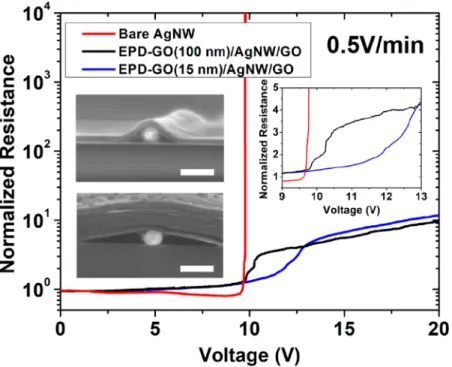
Figure 6.Resistance evolution during voltage ramp across bare NWs and EPD-GO/AgNW/GOfilms with different EPD-GO thicknesses. Values are normalized with respect to each samples’ initial 2PP resistance performance. Inset graph shows magnified view of the main figure in the 9−13 V range. Insets are SEM cross-section images of the two EPD-GO/AgNW/GOfilms used. Scale bar is 100 nm.
that had been covered by EPD-GO (“EPD-GO up” samples) does not exhibit a sulfide peak expected at ∼162 eV, which is evidence that chemical degradation was greatly suppressed. Instead, a signal corresponding to sulfates was detected at ∼168 eV, which originates not from Ag but rather from GO. This was confirmed by an XPS scan in the S 2p and Mn 2p region performed on GOfilms only, which identified a peak corresponding to MnSO4 (Figure S9 and Table S1). The residual MnSO4 is expected since KMnO4 and H2SO4 are
commonly used for Hummer’s method, the solution-based exfoliation of GO.46,47Therefore, no XPS peak related to Ag corrosion product could be identified in the case of “EPD-GO up” samples. Also, the larger sulfate peak observed for “Dip-GO up” samples may be a combined signal originating from both Ag2SO4or Ag2SO3and MnSO4. In summary, the results show that Ag corrosion has been prevented by the exceptional gas-barrier properties of the seamless EPD-GO that impeded transport of corroding gas species to the underlying NW network.48,49
To evaluate the stability under even harsher environment, we also subjected bare networks and doubled-side GO protected networks under 80 °C and 80% relative humidity for 7 days. Such a test was conducted in a similar fashion as the one reported inFigure 5a, except we used a humidity chamber to have a more precise and more reproducible control over the environment in such harsh conditions. The relative humidity variations during the test are reported in Figure S7b. The variation in resistance during 7 days of storage in those conditions is reported in Figure 5b. Results show that the mean sheet resistance of bare AgNWs rapidly increases by 12 times after 7 days due to high humidity that accelerates sulfidation. This is accompanied by increasing variation of sheet resistance within the sample, represented by increasing variance. In contrast, samples where Dip-GO and EPD-GO (15 nm) were facing up demonstrated significant chemical stability even in such harsh conditions, evidenced by a mere 2.4-fold and 1.4-fold increase in the mean sheet resistance, respectively. The fact that we observe such chemical stability at high humidity conditions even though GO is hydrophilic indicates that GO impedes the penetration of sulfuric gas species through AgNWs, as also suggested by previous studies.17,30
3.5. Electrical Stability. The electrical stability of an AgNW-based transparent electrode is another important aspect of its overall robustness, particularly for transparent heater applications where DC voltage is applied to induce high temperature by Joule heating. In particular, it is of interest to delay and mitigate the abrupt failure experienced by AgNW-based networks above a certain voltage, which has been well-documented in prior studies.50Therefore, to fully evaluate the stability and reliability of our composite EPD-GO/AgNW/GO electrode, we measured its electrical resistance in situ while a linear voltage ramp (0.5 V/min) was applied. For the sake of clarity, normalization was done with respect to each samples’ initial two-probe (2PP) resistance values. More details about the experimental setup can be found insection 2.3.
Figure 6 shows that the uncoated AgNW networks’
resistance reduces slightly with voltage up to 5 V, followed by a steeper reduction until 9.5 V, andfinally diverges to more than∼105times its original resistance over the course of only
∼20 s. The reduction of resistance can be attributed to NW junction optimization occurring due to Joule heating. However, a more intense Joule heating at higher applied
voltages will lead to the catastrophic failure caused by the spheroidization of NWs due to Rayleigh instability.50A recent contribution by Sannicolo et al.38 explains the resistance divergence by the initiation of a defect (or hot spot) induced by Joule heating, followed by the propagation of a crack parallel to the bias electrode stimulated by the constriction of currentflow to the extremities of the initial defect. This “crack” composed of spheroidized NWs acts as an insulating region in the NW network that causes the measured resistance to diverge.
With EPD-GO/AgNW/GO samples, a different behavior was observed where abrupt divergence of the electrical resistance is prevented. Figure 6 shows that at the initial stages of ramping the resistance of EPD-GO/AgNW/GO linearly increases, corresponding to the intrinsic resistivity increase of AgNWs by electron−phonon scattering.51 Unlike bare AgNW networks, the resistance does not decrease for EPD-GO/AgNW/GO. This is further indication that the NW junctions are well-optimized by GO encapsulation, mitigating the need for thermal treatment to further weld the nanowires. An interesting behavior is observed as the voltage is ramped past 9.75 V. Here, the AgNW network undergoes an initial degradation as apparent from the deviation of the curves from the initial linear trend, but unlike in bare AgNWs, a complete loss of conductivity is prevented. Specifically, we have observed that the failure behavior depends on the thickness of EPD-GO layer covering the NW network. The inset ofFigure 6shows a close-up of the main plot in the range 9−13 V. For 100 nm thick EPD-GO, the resistance deviates from the original linear dependence from ∼9.75 V onward, increasing to 3 times its initial value at∼10.5 V over the course of ∼90 s. Interestingly, for 15 nm thick EPD-GO, the initial deviation from the linear behavior occurs at a slightly higher voltage around∼11 V and increases to 4 times its initial value at∼13 V over the course of ∼240 s. Therefore, we observe that the presence of EPD-GO slows down the initial NW failure compared to that of bare NWs, and thinner EPD-GO coating results in a higher failure onset voltage as well as a more gradual failure behavior. After this initial damage, both EPD-GO/AgNW/GO samples undergo slower increase in resistance up to 20 V. Even at 20 V, the electrodes exhibited a fairly low resistance near∼150 Ω, a 10-fold increase from its original resistance. In the following paragraphs, we propose and discuss some mechanisms that are most likely to be responsible for our observation.
The observed delay in the onset of electrical degradation as well as the impeded degradation occurring in the early stages of electrical resistance increase may originate from two main mechanisms. First, the presence of EPD-GO and Dip-GO surrounding the NWs allows additional heat conduction pathways for the NWs, which helps dissipate the power generated by Joule heating. For an uncoated AgNW network under voltage bias, it has been demonstrated that the increase in temperature of the network is counterbalanced by heat losses in the substrate via thermal conduction, while the rest is lost via radiation and convection.50,52 In the case of GO-sandwiched AgNW networks, we speculate that the presence of EPD-GO and Dip-GO surrounding the NWs allows additional heat dissipation pathways for the NWs. The overall result is that AgNWs can support higher input voltage before reaching the temperature at which spheroidization is supposed to occur. Second, the presence of GO coating is also expected to slow down the AgNW spheroidization process by hindering atomic surface diffusion. For instance, it is known from previous
studies that a conformal oxide coating on AgNWs drastically reduces the surface diffusivity of Ag atoms such that AgNW can sustain higher temperature and failure is initialized at higher voltages.14,15,53
As pointed out before inFigure 6, the onset of failure was delayed only for the EPD-GO/AgNW/GOfilm with 15 nm EPD-GO and not for 100 nm EPD-GO. This may be attributed to the different degrees of conformality of EPD-GO surrounding the AgNWs according to the EPD-EPD-GO thickness. From the inset SEM images ofFigure 6, it can be seen that the thinner GOfilm can wrap around a larger AgNW surface area compared to its thicker counterpart. In general, deflections of thin membranes under a given load will vary as δ = KP/Et3 where δ is the deflection, P is the load, E is the Young’s modulus, t is the film thickness, and K is a geometrical prefactor. Although recent micromechanical studies show that the Young’s modulus of GO nanosheets is thickness-depend-ent, increasing for thinner GO films, the variation is not expected to significantly affect the strong δ ∼ t−3dependence. For instance, Cao et al.54report E = 204 GPa for 75 nm GO and E = 291 GPa for 24 nm GO. Given these parameters, under a given load, the displacement of the 75 nmfilm will be 20 times less than that of the 24 nmfilm. In our case, the load mainly originates from the capillary force induced by water evaporation during drying of thefilm after transfer. The strong influence of the thickness on the film’s ability to be deflected is consistent with the increase in GO layer conformality over AgNW when minimizing the GO thickness. Also, the more tightly covered the AgNWs are, the more resilient they will be to spheroidization, which also explains the shift in the voltage failure observed in the thinner GO case. Use of thinner EPD-GO to improve the conformality could also minimize the observed loss in transparency. Further improvement of the conformality could be explored through the use of hot rolling press, for instance.55
Finally, beyond the change in behavior observed in the early stages of degradation (8−13 V), the slow increase in resistance observed at even higher voltages (13−20 V) can be explained as follows. Visual inspection of the EPD-GO/AgNW/GO electrode after completion of the voltage ramp test shows a darkened region localized at the center where the electrical crack has been initiated (Figure S11b), and this corresponds to the region where maximum temperature higher than 250 °C was recorded with an IR camera (Figure S10). Because of this intense heat, NWs have spheroidized to a certain degree at this darkened area, while the NWs at the undarkened area were relatively intact (Figure S11a,c). XPS analysis performed at the end of the voltage ramp shows that this darkening is due to the partial thermal reduction of GO layers, as depicted inFigure
S11d−f and Table S2. The survey scan indeed indicates a
higher C/O ratio for the darkened region as well as a prominent increase in the carbon sp2peak in the C 1s scan. This is in line with recent heating studies of bare GOfilms which show that near 170°C graphitic domains grow in size to the point when percolative electronic transport becomes possible, accompanied by sheet resistance reduction by 5 orders of magnitude.56,57 Therefore, it is apparent that the center region of the GO coating is at least partially reduced during voltage ramp and plays a crucial role in preventing resistance divergence by acting as an additional current pathway. Therefore, we propose that the avoidance of resistance divergence at higher voltages (i.e., V > 13 V) is thanks to the reduction of GO sheets acting as an electrical
bridge across spheroidized AgNW areas. In short, it can be seen that our GO encapsulation of AgNW networks effectively acts as a buffer that prevents breakdown at high applied voltages.
4. CONCLUSION
By utilizing EPD and dip treatment of GO, we have developed a scalable and solution-based processing method to fabricate resilient EPD-GO/AgNW/GO transparent conductive films capable of being transferred to arbitrary substrates. Structural characterization by SEM shows that the AgNW network is effectively “sandwiched” between two GO layers, with one side covered by a seamless EPD-GO thickness as low as 15 nm and another side by 1−2 layers of GO. The GO encapsulation allows intimate contact between individual AgNW junctions, which effectively reduces the high junction resistance down to 15Ω/sq without relying on high-temperature annealing of the NWs and allows electrical uniformity across the entire film. Simultaneously, the transmittance of thefilm and its haziness were shown to be tunable between 70% and 87% at 550 nm and between 3.6% and 9.2%, respectively, by simply changing the EPD-GO thickness. Importantly, we show that the sufficient thickness and defect-free quality of the EPD-GO film impart exceptional chemical stability to the AgNWs by mitigating spontaneous sulfidation of Ag that leads to conductivity loss. Furthermore, in situ resistance measurements during linear voltage ramp on our films showed that the catastrophic resistance divergence to the MΩ range which is typical of bare AgNW networks was avoided even at a high applied voltage of 20 V. Although this novel electrical stabilization behavior warrants further scrutiny, we believe that the effects of delayed spheroidization of NWs by GO coating, thermal management by heat conduction through GO, and reduction of GO are collectively responsible for the observed behavior.
Thanks to its double-sided structure, our EPD-GO/AgNW/ GO transparent electrode can offer combined assets, which is favorable toward its compatibility with various devices. On the one hand, the relatively thicker and seamless EPD-GO side offers outstanding chemical and thermal resilience to the outside environment, making the electrode compatible with either high voltage, temperature, or humidity sensitive applications such as transparent heaters or thermochromic windows. On the other hand, the ultrathin Dip-GO layers offer improved stability while still allowing Ohmic contact through any potential adjacent layers, making it compatible with applications sensitive to efficient charge carrier transfer or energy level matching, such as solar cells or LEDs. Depending on the architecture of the target device, one or the other configuration could be preferred and easily controlled during thefilm transfer step. We believe this adds unique versatility to our transparent conductivefilm, and further work may include device integration and device stability evaluation.
■
ASSOCIATED CONTENT*
sı Supporting InformationThe Supporting Information is available free of charge at
https://pubs.acs.org/doi/10.1021/acsami.0c03587.
SEM image of EPD-GO/AgNW/GO with spray coated AgNW, characterization of Dip-GO, AFM character-ization of EPD-GO, haze factor spectra, and additional
data on chemical and electrical stability, including XPS spectra, SEM images, and IR thermal images (PDF)
■
AUTHOR INFORMATIONCorresponding Author
Jeffrey C. Grossman − Department of Materials Science and Engineering, Massachusetts Institute of Technology, Cambridge, Massachusetts 02139, United States;
orcid.org/0000-0003-1281-2359; Email:jcg@mit.edu
Authors
Woo Hyun Chae − Department of Materials Science and Engineering, Massachusetts Institute of Technology, Cambridge, Massachusetts 02139, United States; orcid.org/0000-0001-8385-9491
Thomas Sannicolo − Department of Materials Science and Engineering, Massachusetts Institute of Technology, Cambridge, Massachusetts 02139, United States; orcid.org/0000-0001-9135-1540
Complete contact information is available at: https://pubs.acs.org/10.1021/acsami.0c03587 Notes
The authors declare no competingfinancial interest.
■
ACKNOWLEDGMENTSThe authors acknowledge financial support by Exelon Corporation. This work made use of the MRSEC Shared Experimental Facilities at MIT, supported by the National Science Foundation under Award DMR-1419807. This work was performed in part at the Center for Nanoscale Systems (CNS), a member of the National Nanotechnology Coordi-nated Infrastructure Network (NNCI), which is supported by the National Science Foundation under NSF Award 1541959. CNS is part of Harvard University. The authors also acknowledge Ava Waitz for the development and usage of the spray coating apparatus. The authors also thank Ki-Jana Carter, Adam Trebach, and Jatin Patil for fruitful discussions.
■
REFERENCES(1) Hecht, D. S.; Hu, L.; Irvin, G. Emerging Transparent Electrodes Based on Thin Films of Carbon Nanotubes, Graphene, and Metallic Nanostructures. Adv. Mater. 2011, 23 (13), 1482−1513.
(2) Ellmer, K. Past Achievements and Future Challenges in the Development of Optically Transparent Electrodes. Nat. Photonics 2012, 6 (12), 809−817.
(3) Kim, H.; Gilmore, C. M.; Piqué, A.; Horwitz, J. S.; Mattoussi, H.; Murata, H.; Kafafi, Z. H.; Chrisey, D. B. Electrical, Optical, and Structural Properties of Indium-Tin-Oxide Thin Films for Organic Light-Emitting Devices. J. Appl. Phys. 1999, 86 (11), 6451.
(4) Cairns, D. R.; Witte, R. P.; Sparacin, D. K.; Sachsman, S. M.; Paine, D. C.; Crawford, G. P.; Newton, R. R. Strain-Dependent Electrical Resistance of Tin-Doped Indium Oxide on Polymer Substrates. Appl. Phys. Lett. 2000, 76 (11), 1425.
(5) Lee, J.-Y.; Connor, S. T.; Cui, Y.; Peumans, P. Semitransparent Organic Photovoltaic Cells with Laminated Top Electrode. Nano Lett. 2010, 10 (4), 1276−1279.
(6) Lee, J.-Y.; Connor, S. T.; Cui, Y.; Peumans, P. Solution-Processed Metal Nanowire Mesh Transparent Electrodes. Nano Lett. 2008, 8 (2), 689−692.
(7) Sannicolo, T.; Lagrange, M.; Cabos, A.; Celle, C.; Simonato, J.-P.; Bellet, D. Metallic Nanowire-Based Transparent Electrodes for Next Generation Flexible Devices: A Review. Small 2016, 12 (44), 6052−6075.
(8) Elechiguerra, J. L.; Larios-Lopez, L.; Liu, C.; Garcia-Gutierrez, D.; Camacho-Bragado, A.; Yacaman, M. J. Corrosion at the Nanoscale: The Case of Silver Nanowires and Nanoparticles. Chem. Mater. 2005, 17 (24), 6042−6052.
(9) Langley, D. P.; Lagrange, M.; Giusti, G.; Jiménez, C.; Bréchet, Y.; Nguyen, N. D.; Bellet, D. Metallic Nanowire Networks: Effects of Thermal Annealing on Electrical Resistance. Nanoscale 2014, 6 (22), 13535−13543.
(10) Khaligh, H. H.; Goldthorpe, I. A. Failure of Silver Nanowire Transparent Electrodes under Current Flow. Nanoscale Res. Lett. 2013, 8 (1), 235.
(11) Mayousse, C.; Celle, C.; Fraczkiewicz, A.; Simonato, J.-P. Stability of Silver Nanowire Based Electrodes under Environmental and Electrical Stresses. Nanoscale 2015, 7 (5), 2107−2115.
(12) Chen, D.; Liang, J.; Liu, C.; Saldanha, G.; Zhao, F.; Tong, K.; Liu, J.; Pei, Q. Thermally Stable Silver Nanowire-Polyimide Transparent Electrode Based on Atomic Layer Deposition of Zinc Oxide on Silver Nanowires. Adv. Funct. Mater. 2015, 25 (48), 7512− 7520.
(13) Pham, A.-T.; Nguyen, X.-Q.; Tran, D.-H.; Ngoc Phan, V.; Duong, T.-T.; Nguyen, D.-C. Enhancement of the Electrical Properties of Silver Nanowire Transparent Conductive Electrodes by Atomic Layer Deposition Coating with Zinc Oxide. Nano-technology 2016, 27 (33), 335202.
(14) Khan, A.; Nguyen, V. H.; Muñoz-Rojas, D.; Aghazadehchors, S.; Jiménez, C.; Nguyen, N. D.; Bellet, D. Stability Enhancement of Silver Nanowire Networks with Conformal ZnO Coatings Deposited by Atmospheric Pressure Spatial Atomic Layer Deposition. ACS Appl. Mater. Interfaces 2018, 10 (22), 19208−19217.
(15) Nguyen, V. H.; Resende, J.; Papanastasiou, D. T.; Fontanals, N.; Jiménez, C.; Muñoz-Rojas, D.; Bellet, D. Low-Cost Fabrication of Flexible Transparent Electrodes Based on Al Doped ZnO and Silver Nanowire Nanocomposites: Impact of the Network Density. Nanoscale 2019, 11 (25), 12097−12107.
(16) Kholmanov, I. N.; Stoller, M. D.; Edgeworth, J.; Lee, W. H.; Li, H.; Lee, J.; Barnhart, C.; Potts, J. R.; Piner, R.; Akinwande, D.; Barrick, J. E.; Ruoff, R. S. Nanostructured Hybrid Transparent Conductive Films with Antibacterial Properties. ACS Nano 2012, 6 (6), 5157−5163.
(17) Wu, C.; Jiu, J.; Araki, T.; Koga, H.; Sekitani, T.; Wang, H.; Suganuma, K. Rapid Self-Assembly of Ultrathin Graphene Oxide Film and Application to Silver Nanowire Flexible Transparent Electrodes. RSC Adv. 2016, 6 (19), 15838−15845.
(18) Lai, Y.-T.; Tai, N.-H. One-Step Process for High-Performance, Adhesive, Flexible Transparent Conductive Films Based on p-Type Reduced Graphene Oxides and Silver Nanowires. ACS Appl. Mater. Interfaces 2015, 7 (33), 18553−18559.
(19) Aliprandi, A.; Moreira, T.; Anichini, C.; Stoeckel, M.-A.; Eredia, M.; Sassi, U.; Bruna, M.; Pinheiro, C.; Laia, C. A. T.; Bonacchi, S.; Samorì, P. Hybrid Copper-Nanowire-Reduced-Graphene-Oxide Coat-ings: A “Green Solution” Toward Highly Transparent, Highly Conductive, and Flexible Electrodes for (Opto)Electronics. Adv. Mater. 2017, 29 (41), 1703225.
(20) Alotaibi, F.; Tung, T. T.; Nine, M. J.; Coghlan, C. J.; Losic, D. Silver Nanowires with Pristine Graphene Oxidation Barriers for Stable and High Performance Transparent Conductive Films. ACS Appl. Nano Mater. 2018, 1 (5), 2249−2260.
(21) Moon, I. K.; Kim, J. Il; Lee, H.; Hur, K.; Kim, W. C.; Lee, H. 2D Graphene Oxide Nanosheets as an Adhesive Over-Coating Layer for Flexible Transparent Conductive Electrodes. Sci. Rep. 2013, 3 (1), 1112.
(22) Hwang, B.; Park, M.; Kim, T.; Han, S. M. Effect of RGO Deposition on Chemical and Mechanical Reliability of Ag Nanowire Flexible Transparent Electrode. RSC Adv. 2016, 6 (71), 67389− 67395.
(23) Ricciardulli, A. G.; Yang, S.; Wetzelaer, G.-J. A. H.; Feng, X.; Blom, P. W. M. Hybrid Silver Nanowire and Graphene-Based Solution-Processed Transparent Electrode for Organic Optoelec-tronics. Adv. Funct. Mater. 2018, 28 (14), 1706010.
(24) Soltani-Kordshuli, F.; Zabihi, F.; Eslamian, M. Graphene-Doped PEDOT:PSS Nanocomposite Thin Films Fabricated by Conventional and Substrate Vibration-Assisted Spray Coating (SVASC). Eng. Sci. Technol. an Int. J. 2016, 19 (3), 1216−1223.
(25) Lee, H. J.; Song, Y. S.; An, T. K.; Choi, W. K.; Kim, S. R. Ultrasmooth Transparent Conductive Hybrid Films of Reduced Graphene Oxide and Single-Walled Carbon Nanotube by Ultrasonic Spraying. Synth. Met. 2016, 221, 340−344.
(26) Lian, H.; Qi, L.; Luo, J.; Hu, K. Experimental Study and Mechanism Analysis on the Effect of Substrate Wettability on Graphene Sheets Distribution Morphology within Uniform Printing Droplets. J. Phys.: Condens. Matter 2018, 30 (33), 335001.
(27) Hasan, S. A.; Rigueur, J. L.; Harl, R. R.; Krejci, A. J.; Gonzalo-Juan, I.; Rogers, B. R.; Dickerson, J. H. Transferable Graphene Oxide Films with Tunable Microstructures. ACS Nano 2010, 4 (12), 7367− 7372.
(28) Diba, M.; Fam, D. W. H.; Boccaccini, A. R.; Shaffer, M. S. P. Electrophoretic Deposition of Graphene-Related Materials: A Review of the Fundamentals. Prog. Mater. Sci. 2016, 82, 83−117.
(29) Hasan, S. A.; Kavich, D. W.; Dickerson, J. H. Sacrificial Layer Electrophoretic Deposition of Free-Standing Multilayered Nano-particle Films. Chem. Commun. 2009, 0 (25), 3723.
(30) Liang, J.; Li, L.; Tong, K.; Ren, Z.; Hu, W.; Niu, X.; Chen, Y.; Pei, Q. Silver Nanowire Percolation Network Soldered with Graphene Oxide at Room Temperature and Its Application for Fully Stretchable Polymer Light-Emitting Diodes. ACS Nano 2014, 8 (2), 1590−1600. (31) Diba, M.; García-Gallastegui, A.; Klupp Taylor, R. N.; Pishbin, F.; Ryan, M. P.; Shaffer, M. S. P.; Boccaccini, A. R. Quantitative Evaluation of Electrophoretic Deposition Kinetics of Graphene Oxide. Carbon 2014, 67, 656−661.
(32) Hamaker, H. C. Formation of a Deposit by Electrophoresis. Trans. Faraday Soc. 1940, 35 (0), 279.
(33) Besra, L.; Liu, M. A Review on Fundamentals and Applications of Electrophoretic Deposition (EPD). Prog. Mater. Sci. 2007, 52 (1), 1−61.
(34) Huang, Y. J.; Lai, C. H.; Wu, P. W. Fabrication of Large-Area Colloidal Crystals by Electrophoretic Deposition in Vertical Arrange-ment. Electrochem. Solid-State Lett. 2008, 11 (12), P20.
(35) Lee, D. K.; Kim, S. J.; Kim, Y.; Choi, H.; Kim, D. W.; Jeon, H.; Ahn, C. W.; Lee, J. W.; Jung, H. Graphene Oxide/Carbon Nanotube Bilayer Flexible Membrane for High-Performance Li-S Batteries with Superior Physical and Electrochemical Properties. Adv. Mater. Interfaces 2019, 6 (7), 1801992.
(36) Zhong, Y.; Zhang, X.; He, Y.; Peng, H.; Wang, G.; Xin, G. Simultaneously Armored and Active Graphene for Transparent and Flexible Supercapacitors. Adv. Funct. Mater. 2018, 28, 1801998.
(37) Kumar, P.; Shahzad, F.; Hong, S. M.; Koo, C. M. A Flexible Sandwich Graphene/Silver Nanowires/Graphene Thin Film for High-Performance Electromagnetic Interference Shielding. RSC Adv. 2016, 6 (103), 101283−101287.
(38) Sannicolo, T.; Charvin, N.; Flandin, L.; Kraus, S.; Papanastasiou, D. T.; Celle, C.; Simonato, J.-P.; Muñoz-Rojas, D.; Jiménez, C.; Bellet, D. Electrical Mapping of Silver Nanowire Networks: A Versatile Tool for Imaging Network Homogeneity and Degradation Dynamics during Failure. ACS Nano 2018, 12 (5), 4648−4659.
(39) Chih-Hung, T.; Sui-Ying, H.; Tsung-Wei, H.; Yu-Tang, T.; Yan-Fang, C.; Jhang, Y. H.; Hsieh, L.; Chung-Chih, W.; Yen-Shan, C.; Chieh-Wei, C.; Chung-Chun, L. Influences of Textures in Fluorine-Doped Tin Oxide on Characteristics of Dye-Sensitized Solar Cells. Org. Electron. 2011, 12 (12), 2003−2011.
(40) Compton, O. C.; Cranford, S. W.; Putz, K. W.; An, Z.; Brinson, L. C.; Buehler, M. J.; Nguyen, S. T. Tuning the Mechanical Properties of Graphene Oxide Paper and Its Associated Polymer Nano-composites by Controlling Cooperative Intersheet Hydrogen Bonding. ACS Nano 2012, 6 (3), 2008−2019.
(41) Haacke, G. New Figure of Merit for Transparent Conductors. J. Appl. Phys. 1976, 47 (9), 4086−4089.
(42) Guo, F.; Azimi, H.; Hou, Y.; Przybilla, T.; Hu, M.; Bronnbauer, C.; Langner, S.; Spiecker, E.; Forberich, K.; Brabec, C. J. High-Performance Semitransparent Perovskite Solar Cells with Solution-Processed Silver Nanowires as Top Electrodes. Nanoscale 2015, 7 (5), 1642−1649.
(43) Liang, J.; Li, L.; Niu, X.; Yu, Z.; Pei, Q. Elastomeric Polymer Light-Emitting Devices and Displays. Nat. Photonics 2013, 7 (10), 817−824.
(44) Yoo, B. M.; Shin, H. J.; Yoon, H. W.; Park, H. B. Graphene and Graphene Oxide and Their Uses in Barrier Polymers. J. Appl. Polym. Sci. 2014, 131 (1), 39628.
(45) Kaushik, V. K. XPS Core Level Spectra and Auger Parameters for Some Silver Compounds. J. Electron Spectrosc. Relat. Phenom. 1991, 56 (3), 273−277.
(46) Hummers, W. S.; Offeman, R. E. Preparation of Graphitic Oxide. J. Am. Chem. Soc. 1958, 80 (6), 1339−1339.
(47) Jiangying, Q.; Feng, G.; Quan, Z.; Zhiyu, W.; Han, H.; Beibei, L.; Wubo, W.; Xuzhen, W.; Jieshan, Q. Highly Atom-Economic Synthesis of Graphene/Mn3O4 Hybrid Composites for Electro-chemical Supercapacitors. Nanoscale 2013, 5 (7), 2999.
(48) Su, Y.; Kravets, V. G.; Wong, S. L.; Waters, J.; Geim, A. K.; Nair, R. R. Impermeable Barrier Films and Protective Coatings Based on Reduced Graphene Oxide. Nat. Commun. 2014, 5 (1), 4843.
(49) Yang, Y.-H.; Bolling, L.; Priolo, M. A.; Grunlan, J. C. Super Gas Barrier and Selectivity of Graphene Oxide-Polymer Multilayer Thin Films. Adv. Mater. 2013, 25 (4), 503−508.
(50) Lagrange, M.; Sannicolo, T.; Muñoz-Rojas, D.; Lohan, B. G.; Khan, A.; Anikin, M.; Jiménez, C.; Bruckert, F.; Bréchet, Y.; Bellet, D. Understanding the Mechanisms Leading to Failure in Metallic Nanowire-Based Transparent Heaters, and Solution for Stability Enhancement. Nanotechnology 2017, 28 (5), 055709.
(51) Bid, A.; Bora, A.; Raychaudhuri, A. K. Temperature Dependence of the Resistance of Metallic Nanowires of Diameter⩾ 15 Nm: Applicability of Bloch-Grüneisen Theorem. Phys. Rev. B: Condens. Matter Mater. Phys. 2006, 74 (3), 035426.
(52) Sorel, S.; Bellet, D.; Coleman, J. N. Relationship between Material Properties and Transparent Heater Performance for Both Bulk-like and Percolative Nanostructured Networks. ACS Nano 2014, 8 (5), 4805−4814.
(53) Kwan, Y. C. G.; Le, Q. L.; Huan, C. H. A. Time to Failure Modeling of Silver Nanowire Transparent Conducting Electrodes and Effects of a Reduced Graphene Oxide over Layer. Sol. Energy Mater. Sol. Cells 2016, 144, 102−108.
(54) Cao, C.; Daly, M.; Chen, B.; Howe, J. Y.; Singh, C. V.; Filleter, T.; Sun, Y. Strengthening in Graphene Oxide Nanosheets: Bridging the Gap between Interplanar and Intraplanar Fracture. Nano Lett. 2015, 15 (10), 6528−6534.
(55) Hosseinzadeh Khaligh, H.; Goldthorpe, I. A. Hot-Rolling Nanowire Transparent Electrodes for Surface Roughness Minimiza-tion. Nanoscale Res. Lett. 2014, 9 (1), 310.
(56) Slobodian, O. M.; Lytvyn, P. M.; Nikolenko, A. S.; Naseka, V. M.; Khyzhun, O. Y.; Vasin, A. V.; Sevostianov, S. V.; Nazarov, A. N. Low-Temperature Reduction of Graphene Oxide: Electrical Con-ductance and Scanning Kelvin Probe Force Microscopy. Nanoscale Res. Lett. 2018, 13 (1), 139.
(57) Lipatov, A.; Guinel, M. J.-F.; Muratov, D. S.; Vanyushin, V. O.; Wilson, P. M.; Kolmakov, A.; Sinitskii, A. Low-Temperature Thermal Reduction of Graphene Oxide: In Situ Correlative Structural, Thermal Desorption, and Electrical Transport Measurements. Appl. Phys. Lett. 2018, 112 (5), 053103.