ADAPTIVE CLASSIFICATION OF INTERFERING SIGNALS
IN A SHARED RADIO FREQUENCY ENVIRONMENT
by
GANESH NACHIAPPA RAMASWAMY
Submitted to the Department of Electrical Engineering and Computer Science in partial fulfillment of the requirements for the degrees of
Bachelor of Science a.nd
Master of Science at the
MASSACHUSETTS INSTITUTE OF TECHNOLOGY February, 1992
( Ganesh N. Ramaswamy, 1992
The author hereby grants to MIT permission to reproduce and to distribute copies of this thesis document in whole or in pa.rt.
Signature of Author .. ... ... /Department of Electril Enginering and Computer Science
December 3, 1991
Certified
by
...
:../.
... . ... ...
H
...
Pierre A. Humblet Professor of Electrical Engineering Thesis Supervisor (MIT)
Certified
by
.
.
,T.
... ...
David F. Bantz 1, ger, Portable Systems 4esis ervisor (IBM Research)
Accepted
by....,,-..
./..
.
/../.
.. ... ...
...
.
Campbell L. Searle -airman, Departmental Committee on Graduate Students-Adaptive Classification of Interfering Signals
in a Shared Radio Frequency Environment
by
Ganesh Nachiappa Ramaswamy
Submitted to the Department of Electrical Engineering and Coimpulter Science on December 3, 1991, in partial fulfillment of the requirements for the degrees of
Bachelor of Science and Master of Science
Abstract
In a shared radio frequency environment, where several intentional and unintentional transmitters are expected to co-exist, the ability to identify the source of an arbi-trary interfering signal, using an automated diagnostic tool, is desirable. Treating the subject as a pattern recognition problem in a radio frequency environment, a.
viable scheme for the classification of the interfering signals, with adaptive learning capability, has been developed. The scheme incorporates an architecture for signal acquisition, a strategy for feature extraction, and algorithms for signal classification and learning. To lay the background for current and future work in the subject, a categorization of interfering signals consisting of six categories has been proposed and mathematical models for representative examples from the six categories were con-structed. Performance of the proposed scheme with respect to hardware and software system parameters was evaluated through Monte Carlo simulations.
Thesis Supervisor (MIT): Pierre A. Humblet Title: Professor of Electrical Engineering
Thesis Supervisor (IBM Research): David F. Bantz Title: Manager, Portable Systems
In Lovinlg Memory
of Both of My Grandfathers
ACKNOWLEDGEMENTS
My time with the Portable Systems Group at the IBM Thomas J. Watson Research Center has been a very rewarding experience. I am particularly indebted to David Bantz, my manager for all three of my internship assignments and one of the two supervisors of my thesis, for all the valuable lessons that I had learnt from him. Without exaggeration, I can say that he has made an engineer out of me.
I extend my sincere gratitude to Pierre Humblet, my MIT thesis supervisor, for his understanding and continuous support throughout the six months. I will especially remember the friendly smile with which he always greeted me, the friendly smile that is otherwise hard to find at MIT.
Since the project undertaken was primarily theoretical, it was necessary for me to get periodic feedback on my work. Conversations with Chia-Chi Huang, another member of the Portable Systems Group, were very helpful in this respect.
One of the key aspects of the project was the modelling of some of the known interfering signals. Since no empirical measurements were made for the project, ac-tual measured data obtained from variety of sources played an important role in the construction of the models. I would like to acknowledge Jonathan Cheah (Hughes Net-work Systems), Hap Patterson (Sensormatic Electronics Corporation), Ken Blackard (Virginia Tech), Ted Rappaport (VN-ina Tech), and Bob Cato (IBM Raleigh) for sharing their knowledge concerning some of the known interfering signals with me.
I am grateful to Rick Kaufman (Centralized Scientific Services, IBM Research) for his input on commercial radio frequency components, and to Anand Narasimhan
(RPI) for his suggestions concerning time-frequency analysis during theearly stages of the project.
critical moments of the project and for tolerating my obnoxious use of CPU time, and to all staff of the IBM Research Library for their continuous support in helping me obtain the literature needed for the project.
Throughout my stay at MIT and IBM, I was backed by the support and encour-agement of my family in Malaysia, and my friends at MIT and IBM. The support was essential in my remaining sane during the difficult four-and-a-half years.
To all of you - Terizma kasih, berribu-ribuan terinma kasih' !
Contents
Abstract
Acknowledgements
Introduction
Description of the Problem ... Contributions of the Thesis ... Organization of the Report ...
Part One: Architecture and Algorithms
1 Architecture for Adaptive Signal Classification
1.1 The Concept of a Diagnostic Tool ... 1.2 Strategy for Sampling ...
1.2.1 The Need for a Sampling Strategy ... 1.2.2 Direct Sampling of Bandpass Signals.
1.2.3 Quadrature Sampling of Bandpass Signals ... 1.. Proposed Hardware Architecture ...
1.3.1 The Receiver Front End ... 1.3.2 Sampling and Storage ... 1.3.3 The Processing Unit ... 1.4 Chapter Summary ...
2 Interfering Signals: Definition, Examples, and Mathematical
els
2.1 Definition and Categorization ... 2.1.1 What is an Interfering Signal? ... 2.1.2 The Six Categories of Interfering Signals 2.2 Background for Model Construction ...
2.3 Examples and Mathematical Models ... 2.3.1 Type Al Interfering Signal ... 2.3.2 Type A2 Interfering Signal ...
Mod-25 25 25 27 30 32 33 34 ii iv 1 1 3 4 6 7 7 10 10 12 14 16 16 18 22 23
...
...
...
l . . . . . . . . . . . . . . . . . . . . . . . . . . . . . . . . . . . . . . . . . . . . . . . . .2.3.3 Type B1 Interfering Signal . 2.3.4 Type B2 Interfering Signal . 2.3.5 Type C1 Interfering Signals 2.3.6 Type C2 Interfering Signal . 2.4 Chapter Summary.
3 Strategy for Feature Extraction
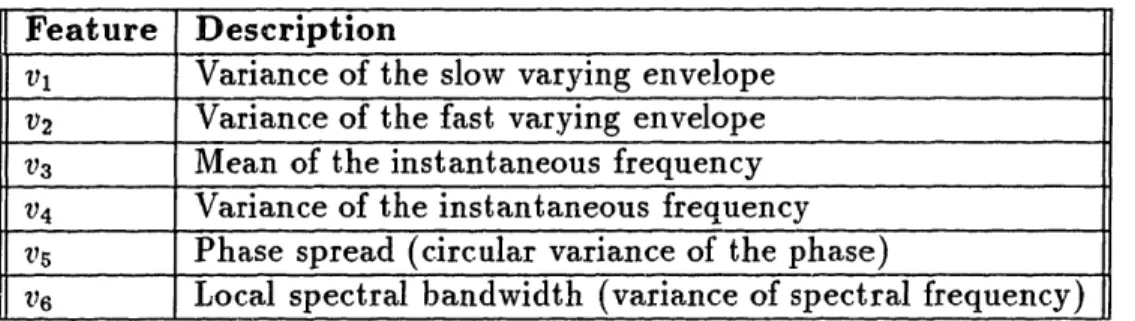
3.1 Constraints and Objectives . ... 3.2 Constructing the Feature Vector ...
3.2.1 The Slow-Varying Envelope and Feature v1
3.2.2 The Rapid-Varying Envelope and Feature v2 3.2.3 Instantaneous Frequency and Features v3 and v4
3.2.4 Estimated Phase and Feature v5 ...
3.2.5 Time Variant Periodogram and Feature v6 . . .
3.3 Chapter Summary ...
4 Adaptive Learning and Signal Classification
4.1 The Search for a Decision Rule . . . .
4.1.1 Constraints and Objectives... 4.1.2 Investigation of Possible Approaches 4.2 Algorithms for Learning and Classification
4.2.1 The Learning Mode ... 4.2.2 The Diagnostic Mode ...
4.3 The Performance of the ML Decision Rule 4.3.1 The Theoretical Bayes Error . 4.4 Chapter Summary ...
Part Two: Performance Evaluation
5 System Implementation
5.1 The Basic Tool Kit ...
5.2 Models for Interfering Signals ... 5.2.1 Simulating the EASD Interference . 5.2.2 Simulating the FM Interference.
5.2.3 Simulating the SSB/FH Interference . 5.2.4 Simulating the MWO Interference. 5.2.5 Simulating the PC interference. 5.2.6 Simulating the GN Interference.
5.2.7 Simulating the Slow-Varying Envelopes 5.3 Procedures for Feature Extraction ..
5.4 Procedures for System Simulation ... 5.5 Chapter Summary ... 34 36 38 42 43 44 44 46 47 48 48 52 .54 55 57
...
57
...
57
58 60 61 62 63 ... 65...
66
67
68...
.69
... . .70
... . .71
..
. . . .71
. . . 71... . .72
. . . . .. ... 7.5... . .76
... . .76
... .- . . . . 77... ....
77
... . .78
. . . . . . . . . . . . . . . . . . . .6 Validating the Scheme
6.1 Simulation Model ... 6.2 Ideal System Performance ... 6.3 Understanding the Feature Vector ... 6.4 Chapter Summary ...
7 System Parameters and System Performance
7.1 The Dynamic Range of the Sampling Module 7.2 Duration of Observation ...
7.3 Frequency and Phase Jitters ... 7.3.1 Frequency Jitter.
7.3.2 Phase Jitter.
7.4 Training Set Size ...
7.5 Putting the Parameters Together ... 7.6 Chapter Summary ...
8 Open Problems Bibliography
A Narrowband Signal Acquisition
B Procedures for Interfering Signal Simulation and Classification
79 79 81 84 90 91 91 94 96 97 98 99 102 103 104 107 115 118 ... ... . . . . ... . . . . ... ... ... ... . . . . . . . . .
List of Figures
1-1 Proposed Scheme for Interference Diagnosis .. ... 9
1-2 The Receiver Front End ... 17
1-3 Sampling and Storage ... 18
2-1 Proposed State Model for Microwave Oven Interference ... 36
6-1 The Simulation Process ... 80 A-1 The Optional Hardware Module for Narrowband Signal Acquisition . 116
List of Tables
2-1 Summary of the Six Models of Interfering Signals ... 3-1 Summary of the Six Components of the Feature Vector v .
6-1 6-2 6-3 6-4 6-5 6-6 6-7 6-8 6-9 6-10 7-1 7-2 7-3 7-4 7-5 7-6 7-7 7-8 7-9 7-10 7-11
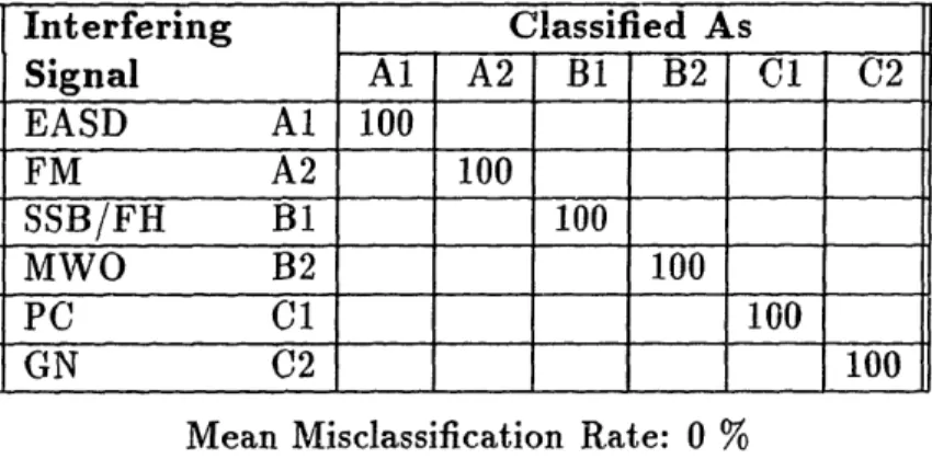
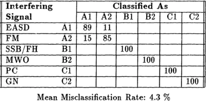
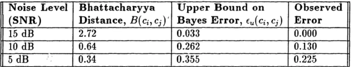
Ideal System Performance at 15 dB SNR. Ideal System Performance at 10 dB SNR. Ideal System Performance at 5 dB SNR ... Confusion Between EASD and FM Signals . System Performance with Feature v1 Removed.
System Performance with Feature V2 Removed.
System Performance with Feature v3 Removed.
System Performance with Feature v4 Removed.
System Performance with Feature v5 Removed.
System Performance with Feature v6 Removed.
System Performance with 8-bit Digitization . . . System Performance with 6-bit Digitization
System Performance with 4-bit Digitization [;... System Performance with L = 1500
System Performance with Frequency Jitter . System Performance with Phase Jitter ... System Performance with N = 100 ... System Performance with N = 50 ... System Performance with N = 25 ... System Performance with N = 10 ... Performance of a Non-ideal System ...
43 56 .. .. . .. . . ... .82 .. ... .. . . ... .83 83 84 85 ... ... 86 87
...
....
... .88
88 89 92 93 93 94 97 99 1.00 101 101 102 103 !,1i . . . . . . . . . . . .Introduction
Upon reading the title of the thesis, several questions may come to the mind of the reader. What is a shared radio frequency environment? Why are we interested in adaptive classification of interfering signals? How can we adaptively classify the interfering signals?
The first two questions will be answered in this introductory chapter. The answer to the third question will be the subject of the thesis.
Description of the Problem
A shared radio frequency environment is a public-use frequency band where several intentional and unintentional transmitters are expected to co-exist. Unlike a con-ventional frequency band with one permitted user, where the interference is usually treated as Gaussian noise, the problem of interference is much more complicated in a shared frequency band because of the presence of several permitted users, transmit-ting a wide variety of signals, including transient or otherwise time-varying signals.
Examples of shared frequency bands are the 902-928 MHz, 2400-2,483.5 MhIz, and 5,725-5,875 MHz bands2 in the United States [61]. Allocations for spectrum use in these bands have been made by the Federal Communications Commission (FCC),
under the provisions for Radio Frequency Devices (Part 15), Industrial, Scientific, and Medical Equipment (Part 18) and Amateur Radio Stations. Transmitters operating under Part 15 require no license, but are neither afforded interference protection from
2
Hereinafter these three frequency bands will be referred to as the bands centered at 915 MIIz, 2.44 GHz, and 5.8 GHz, respectively.
existing and future licensed operations nor from any other Part 15 devices.
In addition to the indoor radio networks employing spread spectrum signalling, authorization for which was recently provided under Part 15 of the FCC rules [55], a variety of intentional and unintentional transmitters use all or part of the three bands. Examples of such users are amateur radio stations, electronic article surveillance systems, microwave ovens, photocopiers, elevator switches, garage door openers, toy walkie-talkies, RF welding equipment, diathermy, and other communications and
non-communications equipment [6], [14], [41], [50], [57].
Interference from other sources using the same frequency band is considered to be one of the major impairments to the successful operation of indoor radio systems [34]. However, our concern in this thesis is not with methods to counter such interference, since this subject is discussed in many recent textbooks on spread spectrum systems, including [74].
Our focus in this project will be to develop a scheme to identify the source of an arbitrary interfering signal'. Such a scheme can then be incorporated into an
ato-mated diagnostic tool, capable of performing interference diagnosis. The diagnostic
tool can be used in several circumstances, for example to survey a given environment prior to installing a radio network (perhaps to find a suitable location for the base station of the network), or to identify the source of interference when a radio link fails due to interference (such that a remedy could be found), or to monitor a shared radio frequency environment on a regular basis and avoid potential radio link failures. The diagnostic tool will provide advice automatically, relieving the pressure to perform the diagnosis manually, and eliminating the need for an expert human engineer.
We have motivated the need for interfering signal classification. But why are we interested in making the classification process adaptive? If the classification process is specific to only a given set of interfering signals in a given environment, the at-tractiveness of the diagnostic tool will disappear when new sources of interference
3
In addition to interference diagnosis for shared radio frequency environments, the developed scheme could also be adapted to identify illegal users in radio frequency environments with one user, or to perform interference diagnosis for other problems involving transient and random signals, like interference diagnosis for power-lines.
are discovered. Such discovery of new interference, or a new behavior of a known interference is not at all unlikely since the spectrum in use is a shared spectrum for which no license is required, and users may appear and disappear unpredictably. Hence, adaptive learning capability of the tool would allow the user to update the tool whenever necessary, with minimal input from the user.
Therefo:e, we set our objectives as to develop a scheme for interfering signal classification, with adaptive learning capability. Such a scheme will incorporate a viable architecture for the diagnostic tool and the necessary algorithms to perform the learning and diagnosis. In order to motivate the future hardware implementation of developed architecture and algorithms, the performance of the proposed scheme and the significance of some of the system parameters will be characterized analytically and through simulations.
Contributions of the Thesis
The problem to be addressed in the thesis could be described as a pattern classification problem, in a radio frequency environment, involving a variety of signals exhibiting transient and random behavior. Unfortunately, no published prior work has been found for such a problem. The only classification problem that appears to address the radio frequency environment is the problem of modulatioTn recognition. Modulation recognition, which is in fact a subset of the more com, plex problem of interfering signal classification, does not involve difficulties such as the transient nature of many interfering signals, frequency hopping phenomenon, difference in bandwidth between the interfering signals, and general random behavior of most interfering signals. So, the techniques used in modulation recognition, details of which will appear later in the report, are not directly applicable to our problem.
The contributions of the thesis consist of both engineering contributions and
aca-demic contributions. The engineering contributions of the thesis
are:C-The development of an appropriate high-level architecture for the diagnostic tool, that can be supported by the current state of technology.
* The investigation of the sensitivity of system performance with respect to the system parameters.
The academic contributions of the thesis are:
* Categorization of the interfering signals and the modelling of several known interfering signals, which provides the background for current and future work in the subject.
o Development of a strategy for feature extraction, to allow the adaptive classifi-cation of a wide variety of signals
* Tlhe development of the learning and classification stages, and the associated identification of a viable decision rule among known decision rules for pattern classification, such that a simple algorithm for the adaptive learning process is possible.
The outcome of the project consists of a viable scheme for interfering signal classi-fication, whose performance has been verified through simulations, and a set of initial system parameters to provide the background for the future hardware implementation of the proposed scheme.
Organization of the Report
The remainder of this report is divided into two parts. Part I reports the development of the architecture and algorithms for interfering signal classification, and Part II illustrates the performance evaluation of the proposed system that was performed by simulating the interfering signals and the learning and classification stages.
Part I consists of four chapters. In Chapter 1, the development of the architec-ture for adaptive signal classification is reported, with particular emphasis on the signal acquisition techniques. In Chapter 2, the term interfering signal is defined, a categorization of the interfering signals consisting of six categories is proposed, and mathematical models are constructed for examples drawn from each of the categories.
Chapter 3 addresses the topic of a suitable strategy for feature extraction, using the background provided by the models of Chapter 2. The selection of the six critical features is described and several other features are proposed for future extensions. Chapter 4 concludes Part I by illustrating the process of identifying a suitable deci-sion rule, and the development of the learning and classification stages.
Part II also consists of four chapters. Chapter 5 describes the system implemen-tation through simulation, which primarily involves the discussion on the software packages that were written for the Monte Carlo simulation of interfering signals, and for the implementation of the learning and classification stages. In Chapter 6, a model for the simulation process is discussed, and the results of initial experiments performed to validate the scheme, and to understand the significance of the features extracted, are reported. Chapter 7 continues with the experiments by evaluating the system performance with respect to software and hardware system parameters. Chapter 8 concludes the report by summarizing the accomplishments of the thesis and providing directions for future work.
There are two appendices to the report. Appendix A contains a description on an optional hardware module that would improve the performance of the system when the encountered interfering signal is a narrowband signal. Appendix B contains the actual documented software packages written for the performance evaluation.
PART I:
ARCHITECTURE AND ALGORITHMS
_ __
Chapter 1
Architecture for Adaptive Signal
Classification
We begin this chapter by discussing the basic functional specifications for the diag-nostic tool proposed in the introduction to this report, and we derive a scheme for interfering signal classification that would satisfy the requirements of the tool. Then we illustrate the challenge involved in the signal acquisition, and motivate the use of the quadrature sampling of bandpass signals. We proceed to develop a viable hard-ware architecture for adaptive signal classification, identifying the significant system parameters that will be later addressed in this report. Appendix A of this report concerns an optional hardware module that can be used to improve the performance of the system if several types of narrowband interfering signals exist.
1.1 The Concept of a Diagnostic Tool
In this section we discuss the proposed concept of a diagnostic tool for interference diagnosis, which is the primary application of the signal classification architecture and algorithms to be developed in this project. Understanding the requirements of the tool would facilitate the development of the necessary system design theory.
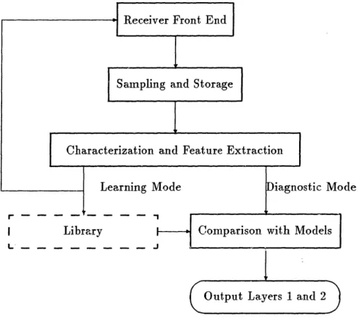
We would like the~tool to have the capability of correctly classifying the observed signal if the signal has been previously encountered by the tool, and the capability of
adaptive learning if the signal is new. We therefore conclude that the diagnostic tool should have two operating modes - the Learn7ing mode and the Diagnostic mode.
The Learning mode will be used during the installation of the tool in a new environment, and whenever a new source is found. The Learning mode should require minimal supervision from the user. In this mode, the tool will collect data. from the source in consideration, compute the necessary parameters to identify the source in the future and store these parameters in a system library. The internal processing involved will not be transparent to the user.
During the Diagnostic mode, the tool captures the signal encountered, derives a parametric representation of the data, compares it with the models stored in the system library, and finally provides the user with the classification of tile signal. The tool will have the capability of estimating the likelihood of the diagnosis being correct, and if the probability happens to be lower than a predetermined threshold, it will declare a no diagnosis state, which may correspond to the discovery of a new source, or equivalently, the discovery of a new behavior of a known source. If the user desires, he may switch to the learning mode at this point to update the system library. The no-diagnosis state may also correspond to several other situations, for example excessive background noise, or the presence of more than one interfering signal'.
The diagnostic tool may take one of several forms. It could be a stand-alone
diagnostic tool, in which case it will have its own built in memory and processing
power. It could be a diagnostic sub-system that can be interfaced to a personal computer, in which case the sub-system will have the necessary hardware for signal acquisition and storage, but will use the processing facilities of the host system. The diagnostic sub-system can also be incorporated into a host system in the form of a communications test set (for an example of a test set, see [31]), which would otherwise not have the hardware or the software needed to perform interference diagnosis.
Further development of functional specifications for the tool is beyond the scope of this project. Based on the discussion in the preceding paragraphs, we propose the
'In this project we will be concerned with classification when only one interfering signal is present.
The extension of the work to include classification when multiple sources are present will be discussed briefly in Chapter 8, as a suggested topic for future work.
,de
Figure 1-1: Proposed Scheme for Interference Diagnosis scheme illustrated in Figure 1-1 for the interference diagnosis.
We recognize that the functions of the tool fall into two broad categories: signal
acquisition and signal analysis. Signal acquisition is a hardware problem, and in
Figure 1-1, the modules marked Receiver Front End and Sampling and Storage fall in this category. The Receiver Front End is responsible for capturing the signals in the band of interest and submitting the signal to the Sampling and Storage module. The Sampling and Storage module, as the name implies, is responsible for sampling and storage of the acquired signals.
Signal analysis is an algorithmic problem. The two modules in Figure 1-1, marked as Characterization and Featare Etraction and Comparison with Models will be employed for the purpose of signal analysis. Although the two modules could be implemented strictly in hardware, we prefer to implement them in software. The
Characterization and Feature Extractioil module is responsible for transforming the acquired data (which may consist of several thousand samples), for the purpose of dimension reduction, into a feature vector consisting of features extracted from the acquired data. The Comparison with Models module is responsible for comparing the received feature vector with models stored in the system library and provide an output. The output will have two layers. Outpt Layer will consist of the identification of the most likely source among the models currently in the system library, or the no-diagnosis state if the likelihood of the most likely interfering signal is lower than a predetermined threshold. Otput Layer 2 provides the actual values of the features computed (which will otherwise not be transparent to the user), for independent evaluation of the diagnosis by the curious user.
As can be seen from Figure 1-1, all four of the modules are involved in the Di-agnostic mode. In the Learning mode, only the first three of the modules are used. The loop in the Learning mode indicates that repeated measurements will be made in order to characterize the distribution of the feature vectors obtained. Therefore, there is an intermediate processing of the acquired feature vectors prior to storing the information in the Library, which we refer to as the adaptive learning process. This processing stage is not explicitly shown in Figure 1-1.
The system design issues that are algorithmic in nature will be discussed in Chap-ters 3, and 4. In the following section, we address the challenge of an appropriate sampling technique which can then be used to develop a suitable hardware architec-ture for diagnostic tool.
1.2 Strategy for Sampling
1.2.1 The Need for a Sampling Strategy
It is common to use a spectrum analyzer with a. broadband antenna, to perform radio frequency measurements [4], [22], [69]. Unfortunately, such an approach to signal acquisition is insufficient for our purpose. Most commercially ava.ilable spectrum analyzers are scanning analyzers (also known as non-real-time analyzers) that is not
tuned to the entire spectrum in consideration at once, but only to a single frequency at one time. The analyzer scans through the spectrum, and since it must wait to tune to a frequency, the phenomenon under test must be repetitive or it may not be detected [30]. For example, consider a unmodulated carrier that is hopping in frequency, thereby virtually occupying a wider bandwidth. In order to accurately
capture this signal, the spectrum analyzer's sweep rates have to be synchronized with respect to the hopping rate of the signal. There are two problems with this. First, the spectrum analyzer may not have a high enough sweep rate to accommodate high hopping rates of the signal. Second, prior knowledge of the hopping pattern of the signal is necessary to establish sweep rates that are synchronized, and since our purpose is to classify an unknown signal, such knowledge of time-varying behavior of interfering signals will not be available prior to the classification.
The purpose of the above discussion is primarily intended to motivate the fact that in order to accurately capture an unknown signal, which can virtually be anywhere in a given band, the entire band has to be captured simultaneously. We recall that the bands that are of interest to us are the three bands, centered at 915 MHz, 2.44 GIIz, and 5.8 GHz. Since the higher band of 5.8 GHz is currently limited by the cost of technology for consumer products [14], we focus our attention on the two lower bands. Also, since the the 2.44 GHz band has a bandwidth of 83.5 MHz, higher than the bandwidth of the 915 MHz band, we realize that by setting our target for the 2.44 GHz band, the obtained solution can be easily adapted for the 915 MHz band.
We state here the famous sampling theorem due to Shannon (1949):
Theorem 1.1 If a function f(t) contains no frequencies higher than W cps it is
completely determined by giving its ordinates at a series of points spaced (1/2W) s apart.
A proof of the theorem, and its extension to the case of random signals, could be found in [36]. Therefore, by direct application of Theorem 1.1 for the 2.44 GHz band, which has frequency components up to 2.4845 GHz, a sampling rate of almost 5 GHz would be required. Such high sampling rates are unfortunately beyond the scope of the current technology.
Fortunately, since the signal is bandlimited to the permitted frequencies, either because the signal is naturally bandlimited, or because the signal has been bandpass filtered to remove the spectral components that are not in the band of interest, we found solutions to the sampling problem by means of bandpass sampling theorems.
1.2.2 Direct Sampling of Bandpass Signals
Even though a bandpass signal is bandlimited, directly sampling a bandpass signal is more complicated than a bandlimited lowpass signal, because two spectral 3a.nds are involved in the case of bandpass signal, one centered at the positive center frequency of f and another centered at -f,. Since sampling produces replicas of the original spectrum [56], appropriate choice of sampling frequency is necessary to avoid aliasing. There are several theorems that have been discussed in theory that can be used in the selection of the appropriate sampling frequency. One such theorem is the
first-order sampling theorem for bandpass signals, stated below, where the signal is directly
sampled at a lower rate than that predicted by Theorem 1.1.
Theorem 1.2 For a bandpass signal y(t) having spectral components (in Hz) only in
the range
f
- V<Ifl
< fo + W, wheref >
W,
miinimum required samnpling rate (in Hz)to
determine thesignal
for all values of time, by direct sampling of y(t), isgiven by
2(fo + W)
fs(min)
=
2f+
(1.1)
where k is the largest nonnegative integer satisfying
k < W (1.2)
- 2W
For a proof and a detailed treatment of the theorem, see [11]. Discussions on direct sampling of bandpass signals could be found in many recent textbooks, including [12],
[56], [60], [67].
We notice that f(,,miu) in equation (1.1) takes values in the range [4W, 81i'), with
the minimnum value of 4W achieved when (1.2) is satisfied with equality. The value of 4W is precisely twice the bandwidth of the signal, which is the same as the
re-quired minimum sampling frequency for a lowpass signal of equivalent bandwidth. Generalization of the first-order sampling of bandpass signals to second and higher order sampling, where two or more interleaved sequences of equispaced sampling is performed [36], [60], results in a more efficient sampling rate with the minimum rate of twice the bandwidth applicable to any value of TV.
Theorem 1.2 provides, in theory, a method for sampling a bandlimited high fre-quency signal at a much lower rate than that predicted by Theorem 1.1, and this is particularly useful when f is much larger than W. The signal directly reconstructed from the samples of the direct sampling process will correspond a lowpass signal, with a bandwidth of ~f3(·m i), but with the knowledge of fo, the original bandpass signal
can be determined by means of frequency shifting [60].
However, many practical issues arise in implementing this method in hardware. We shall assume, for the convenience of discussion, that (1.2) is satisfied with equality and the sampling rate of 4W is applicable. By employing the direct sampling tech-nique, we will essentially be making an analog-to-digital converter (ADC) running at a rate of 4W, thereby expecting to see a signal that varies in the order of 2W, to digitize a bandpass signal which has frequency components up to f + W.
First, we realize that any jitter in the clock input to the ADC will result in an increased error in quantization because the signal is varying much faster than the sampling rate. Second, there will be a further increase in the sampling error due to the aperture time constraints of real ADCs . For example, the AD90282, a high speed flash 8-bit ADC capable of sampling rates up to 300 MSPS, has an aperture delay of 1.4 ns, and an aperture uncertainty of 3 ps (rms) [2].
The aperture time is the interval between the application of the hold command and the actual opening of the switch within the ADC, and consists of a delay and an uncertainty. While there are methods to compensate for the aperture delay, by means of advancing the hold command by the known value of aperture delay, the aperture uncertainty poses the ultimate limitation. The maximum frequency f,,,n which can be handled with less than one least significant bit (LSB) error, is related
to the number of bits per sample, n, and the aperture uncertainty, rau, by [2]
2-n
fma < -r (1.3)
For the AD9028, the maximum frequency which can be handled with less than 1 LSB error is computed to be approximately 400 MHz, which is much less than frequencies up to 2.4835 GHz that may be encountered in the 2.44 GHz band.
Direct sampling of bandpass signals is not impossible to implement, but imple-mentation using current hardware technology may lead to errors in sampling that are higher than the error that would be encountered in the case of a lowpass signal with equivalent bandwidth. We realize that this error is due to the presence of high frequency components in the bandpass signal, and if we could downconvert the band-pass signal to a lower frequency band, then the error rate would be reduced. This option, leading to another sampling theorem for bandpass signals, will be discussed in the next section.
1.2.3 Quadrature Sampling of Bandpass Signals
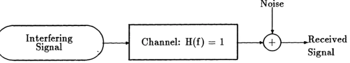
Now, we consider the option of preprocessing the bandpass signal prior to sampling. The preprocessing takes the form of downconverting the bandpass signal to two equiv-alent baseband signals, then sampling these two signals at the rate prescribed by Theorem 1.1.
We state the quadrature sampling theorem for bandpass signals as:
Theorem 1.3 A bandpass signal y(t) having spectral components (in Hz) only in the
range f - W < If < fo + W, where f > W, can be determined from samples of its
two equivalent quadrature baseband components, each sampled uniformly at 21
V.
Proof: Any bandpass signal y(t) may be written as [12], [64]
With
xi(t)
=x(t)
cos[O(t)] and xQ(t) = sin[qb(t)],y(t) = xi(t) cos[27rft] - Q(t) sin[27rfot] (1.5)
Since cos[27rf0t] and sin[2rfot] are real functions, xi(t) and xQ(t) will be real provided
that y(t) is real. Further, since y(t) is has a bandwidth of 2W centered around f,, xz(t) and x.Q(t) will be lowpass signals bandlimited to [-W, W]. By Theorem 1.1, xi(t) and xQ(t) can each be uniquely determined by sampling each of them at 2W. With the knowledge of f,, y(t) can be uniquely determined from the samples of xi(t)
and xQ(t), each sampled at a rate 2W. O
For an alternate derivation of the theorem, see [10]. Since the applicability of Theorem 1.1 has been shown for the case of random signals [36] and since we have only used Theorem 1.1 to prove Theorem 1.3, we realize that Theorem 1.3 can be applied to the case of random bandpass signals.
We will refer to xi(t) and xQ(t) as the in phase (I) and quadrature (Q) components of y(t). By using conventional techniques of downconversion [42], where the bandpass signal y(t) is multiplied with the signals 2 cos(27r.ft) and -2 sin(27rfot) from a local oscillator and then lowpass filtered to retain only the frequency components in the range [-W, W], we can obtain x.(t) and zQ(t), respectively.
We notice that, asqopposed to direct sampling of bandpass signals at a rate of 4W (or higher), now we are able to sample the two quadrature components at 2W each. For the 2.44 GHz band, the bandwidth of 2W corresponds to a value of 83.5 MHz, which can be achieved-by many of the high speed ADCs currently available in the market, including the AD9028 encountered before. By downconverting the bandpass signal into two baseband quadrature components, we have solved the problem induced by the presence of high frequency components. However, we have also introduced additional hardware into the system by the option, and hence additional system parameters.
Having found a suitable sampling strategy, we proceed to discuss a hardware architecture for the diagnostic tool in the next section.
1.3 Proposed Hardware Architecture
The requirements introduced by the need to perform adaptive signal classification introduces no additional hardware complexity. The signal acquisition stage is iden-tical in both the Learning mode and the Diagnostic mode, with the only hardware difference being the repeated measurements needed to characterize the distribution of feature vectors in the Learning mode, which can be achieved by generating an appropriate control signal in software. Therefore, the same hardware can be used for signal acquisition in both of the modes.
There is an added advantage in using the same hardware for both modes, besides being cost efficient. Since the signal acquired in the Learning mode will be subject to the same system parameters (say, for example, the number of bits per sample), as the signal acquired in the Diagnostic mode, the characterization of the distribution of feature vectors in the Learning mode will be a more accurate description of the feature vectors likely to be encountered by a given diagnostic tool in the Diagnostic mode.
Although detailed hardware design for the diagnostic tool is beyond the scope of the paper, we would like to at least outline a high level architecture for the tool. We recall that there were four modules in the scheme proposed in Figure 1-1. We would like to reduce these four modules into three hardware stages, with the two software modules of Characterization and Feature Extraction, and Comparison with Models, combined into a single hardware stage of Processing Unit. In addition to containing the two software modules, the Processing Unit will also be responsible for part of the
control of the signal acquisition process on the one end, and the user interface on the
other end. The three hardware stages are discussed in the following subsections.
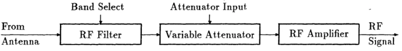
1.3.1 The Receiver Front End
The Receiver Front End takes two inputs, a BAND SELECT control signal from the
Processing Unit to indicate the frequency band that should be captured (either the 915 MHz, 2.44 GHz, or the 5.8 GHz band), and an ATTENUATOR INPUT control signal
From RF Antenna Antenna RF Filter Variable Attenuator RF Amplifier SigalSignal
Figure 1-2: The Receiver Front End
from the Sampling and Storage module, to set the appropriate attenuation level for the encountered signal. It has one output, which is the received Radio Frequency (RF) signal, submitted to the Sampling and Storage module.
A possible implementation of the Receiver Front End is shown in Figure 1-2. The reader should note that the receiver continuously receives RF signals, with possible changes in the attenuation level as prescribed by the ATTENUATOR INPUT control signal, provided that the tool has been turned on, and the band has been selected. Therefore the Receiver Front End need not be aware of the mode of operation.
The band-selection could be achieved by having three bandpass filters with the 3dB cut-off frequencies set at the edges of the three bands we discussed before3 and
by employing the BAND SELECT control signal to choose the appropriate filter. The attenuator is present to adjust the relative strength of the received signal such that the full dynamic range of the analog-to-digital converter in the Sampling and Storage module can be utilized. The attenuator also ensures that the RF amplifier is not driven into saturation. Since different interfering signals may require different attenuation levels, the attenuator should be a variable attenuator. A programmable attenuator may be used for this purpose, provided that its settling time is short compared to the duration of occurrence of the interfering signals that are of interest. If such an attenuator is not available, then several different attenuators, set at different attenuation levels, may be used in parallel, with the selection of the appropriate attenuator made by the ATTENUATOR INPUT control signal.
3Here we are assuming that it is sufficient to observe only the activities within the band, and we will not be concerned with out of band emnissions from neighboring bands.
Attenuator Input
Figure 1-3: Sampling and Storage
Further discussion on the components of a typical radio frequency receiver could be found in handbooks and textbooks on radio frequency surveying, including [69].
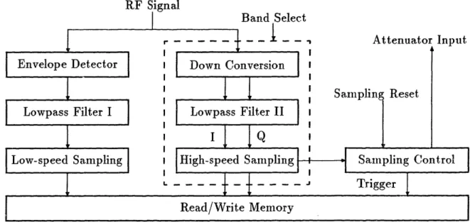
1.3.2 Sampling and Storage
The Sampling and Storage module takes the RF signal from the Receiver Front End, and the control signals BAND SELECT and SAMPLING RESET from the Processing Unit as its inputs, and generates the ATTENUATOR INPUT control signal for the attenuator in the Receiver Front End, and the SAMPLING COMPLETE interrupt signal for the Processing Unit, as its outputs. Like the Receiver Front End, the Sampling and Storage module will also be not aware of the mode of operation, and will faithfully sample and store the signals received whenever the SAMPLING RESET is set by the Processing Unit. Such continuous sampling allows flexible triggering.
A possible implementation of the module is shown in Figure 1-3. The generation of SAMPLING COMPLETE signal is not shown in the figure. Also not shown in the figure is the additional control circuitry to control the transfer of data between the
Processing Unit and the Sampling and Storage Module that may become necessary. In Section 1.2, we saw how a lowpass signal bandlimited to [- W, W] needs a sam-pling rate of only 2W. However, this is only in the ideal case, and in practice usually a higher rate would be required. Oversampling by a factor of 2, thereby employing a sampling rate of 4W as opposed to the ideal sampling rate of 2W, is typically recommended [44]. While a higher sampling rate leads to a greater accuracy in dig-itization, it also makes the acquisition system operate at a higher speed, requiring more memory for the same duration of observation, thereby making the system more expensive. Since further verification of the need for oversampling requires hardware experiments, which is beyond the scope of this project, we shall assume that the factor 2 of oversampling is applicable.
The wideband4 IQ signal acquisition shown in the dotted box in Figure 1-3 is a
direct implementation of Theorem 1.3. The BAND SELECT control signal from the Processing Unit is used to select the appropriate downconversion frequency, lowpass filter bandwidth and the sampling rate, since these three values will be different for different frequency bands. A sinusoid at f,, the center frequency of the band of interest, from a local oscillator can be used as an input to a 900 power splitter, which will generate cos 27rft, and sin 2rfot. These two signals can be multiplied with the incoming RF signal in a frequency mixer, and lowpass filtered (using Lowpass Filter II in Figure 1-3) to retain only the frequency components in the range [-W, IW] where
2W is the bandwidth of the band being captured. The resulting I and Q signal, as
defined in Section 1.2.3 of this chapter, can be digitized using a high speed ADC as discussed before. Taking into consideration the factor 2 of oversampling discussed above, a sampling rate of 167 MHz is suitable for the 2.44 GHz band.
The reader may be surprised to see the blocks labelled Envelope Detector, Lowpass
Filter I and Low-speed Sampling, in Figure 1-3. These three blocks will be used
to acquire what we shall refer to as the slow-varying envelope of the encountered interfering signal. As we shall see in Chapter 2, there are devices such as Microwave
4Appendix A describes an optional hardware module that can be added to the system to improve performance in the special case where the signal encountered is a narrowband signal. So, we use the word wideband here to distinguish between the two hardware modules
Ovens that emit RF energy only during one half of the 60 Hz cycle of the power supply. Hence, we are interested in detecting the presence or absence of a "square wave" at 60 Hz, the slow-varying envelope, which is a piece of information which we suspect would be useful in identifying the signal. Since the 60 Hz frequency corresponds to a period of 16.7 ms, in order to compute the slow-varying envelope ill software from the wideband I and Q samples that are sampled at a high frequency, a huge amount of sampling memory (in the order of Megabytes) will be needed. So, we have elected to compute the slow-varying envelope in hardware using an envelope detector, a lowpass filter, and an ADC sampling at a much slower rate. The envelope detector is a rectifier circuit, commonly described in many textbooks, including [42]. Ideally, we would like to the slow-varying envelope to be a square wave at 60 Hz for signals from devices exhibiting the 60 Hz behavior, and a pure DC value for other signals. However, a large bandwidth will be required to accurately characterize a square wave [42], and this will unfortunately permit high frequency components to corrupt the slow-varying envelope. But since we are only interested in an approximate shape of the envelope, we realize that capturing up to, say, the fifth harmonic of the square wave should be sufficient. Therefore, the time constant of the envelope detector should be sufficiently large to remove all high frequency components, and to further ensure that only the frequency components below the fifth harmonic of the square wave remains, we include a lowpass filter with a 3 dB bandwidth of 300 Hz. The slow envelope can be sampled at 1200 Hz, corresponding to a factor 2 of oversalmpling, and the duration of observation needs to be only 16.7 ims, which is the period of a 60Hz signal, thereby requiring only 20 samples per observation.
The block labelled Sampling Control is responsible for generating the ATTENU-ATOR INPUT control signal to set the attenuation level in the Receiver Front End, and the TRIGGER signal to start storing the sampled signal. After the band has been selected and the SAMPLING RESET has been set, the module will be continuously sampling the received signal. Initially the attenuation level should set to a low level, such that any signal above the mean thermal noise may be detected. By observing a small number of samples, the amplitude of the received signal will be compared to
a threshold value, and if the threshold is exceeded then an interfering signal will be assumed to be present. Then, based on the first few samples observed, the Sampling Control will make a guess as to what the appropriate level of attenuation should be, and after a delay corresponding to the settling time of the attenuator, the TRIGGER
signal will be generated to start the storage of the samples. Upon completion of the storage, the SAMPLING COMPLETE interrupt signal will be sent to the Processing Unit.
There are several system parameters in the Sampling and Storage module that may have a significant influence on the performance of the diagnostic tool. With respect to the slow envelope acquisition, we have essentially resolved, in theory, the issue of the lowpass filter bandwidth, and the sampling rate. Further verification of the method and the analysis related to the system parameters have to be performed through actual hardware experiments. Likewise, in the case of the wideband I and Q signal acquisition, again we have resolved the issue of the lowpass filter bandwidth and the sampling rate, leaving further verification (involving issues like the possible non-linearity of the mixer, and the non-ideal behavior of the filters) up to future hardware experiments. In the case of the Sampling Control, we only outlined a general scheme that can be used to control the sampling process, and we realize that a significant amount of design and verification has to be performed. In particular, the appropriate threshold for comparison of the signal amplitude, the exact number of samples to be used in generating the control signals, and the criteria for generating the control signals are expected to important.
There are three other parameters of the system that we would be able to analyze in theory and through simulations. These parameters are:
* The dynamic range of the sampling system * The duration of observation
* The sensitivity of the system to frequency and phase jitters from the local oscillator circuitry used in the downconversion process
wide-band I and Q signal acquisition. The remaining two issues are related to only the wideband I and Q signal acquisition, since we have resolved the issue of duration of observation (i.e. 20 samples at 1200 Hz) for the slow varying envelope, and there is no downconversion involved.
The dynamic range issue will be addressed from the viewpoint of the number of bits per sample required for acceptable performance, keeping in mind that the attenuator can be used to utilize the maximum dynamic range of the ADC. The duration of observation is related to both the sampling rate and the record length (the number of samples per observation), but since we have set the sampling rate (recall the factor 2 of oversampling), only the record length is a variable in our investigation. Since the local oscillator circuitry used in the IQ downconversion process may exhibit frequency and phase jitters, we would like to model these jitters as stochastic processes to gain an understanding of how sensitive the system performance will be to the non-ideal behavior of the system. These topics will be addressed in Part II of this report.
1.3.3 The Processing Unit
As we saw in Section 1.1 of this chapter, the diagnostic tool can take one of several forms, and the required hardware for the Processing Unit will be different for each implementation. In any case, the Processing Unit should have the memory needed to contain the system library, but since the feature vector computed is expected to be much smaller i-dimension than the actual data, only a small storage space will be needed. The memory allocated for the system library should allow both READ and WRITE operations, since data will be written during the Learning mode and read during the Diagnostic mode.
In addition to the primary responsibility of performing the necessary signal analy-sis during the two modes of operation, the Processing Unit will also be responsible for the control of the tool (with the exception of the ATTENUATOR INPUT control signal generated by the Sampling and Storage Module), and for the interface with the user. After the entry of the desired inputs from the user, the Processing Unit will generate the BAND SELECT and SAMPLING RESET signals previously discussed. Upon
receiving the SAMPLING COMPLETE interrupt signal from the Sampling and Storage
module, the Processing Unit will read in the data acquired, and perform the necessary signal analysis. The Processing Unit will have the knowledge of N, the number of independent measurements needed for the Learning Mode, and is solely responsible for generating the required number of SAMPLING RESET signals and for keeping track of the number of measurements completed at any given time during the Learning Mode. Another responsibility of the unit is to update the system library after the adaptive learning process. The Processing Unit is also responsible for providing the two output layers (the results of the diagnosis) through the selected used-interface.
Hardware parameters of the Processing Unit relate to the processing speed of the of the system, which is a customer satisfaction issue, and therefore will not be ad-dressed in this project. However, there are several software parameters that affect the performance of the system, including the required number of independent mnea-surements to be made during the Learning mode, the specific features that should be included in the feature vector, the algorithm for adaptive learning and classification of the interfering signals, and the value of Pth, the threshold value for the likelihood of the most likely signal, below which the diagnostic tool should declare the no-diagnosis state.
Since the Processing Unit is the only module that is aware of the mode of oper-ation, the requirement of making the signal classification adaptive introduces severe constraints in the form of appropriate feature selection methodology and classifica-tion algorithms. Theoretical issues related to the selecclassifica-tion of these parameters will be discussed in detail in Chapters 3 and 4, and the related performance evaluation will be discussed in Part II of this report.
1.4 Chapter Summary
This chapter began Part I of this report, by discussing several issues related to the architecture for adaptive signal classification. We introduced the reader to details concerning the proposed application of the architecture and algorithms developed in
this project, in the form of a diagnostic tool for interference diagnosis. We recognized the difficulties in signal acquisition, and we explored strategies for sampling. We then discussed the details of the Receiver Front End, and the Sampling and Storage module. We also discussed briefly the hardware aspects of the Processing Unit which incorporates the two software modules of Characterization and Feature Extraction, and Comparison with Models. Since the design of these two modules are primarily algorithmic, the necessary algorithms will be developed in Chapters 3 and 4. In Chapter 2, we will proceed to develop models of interfering signals, keeping in mind that the signal acquisition architecture will affect the form of the received signal. The system hardware system parameters identified in this chapter will be further addressed in our performance evaluation process, which is reported in Part II. Appendix A of this report contains a brief description of an optional hardware module that could be added to improve the performance when the encountered signal occupies a bandwidth much narrower than the bandwidth of the captured band.
Chapter 2
Interfering Signals: Definition,
Examples, and Mathematical
Models
The objective of this chapter is to gain an understanding of how a variety of received interfering signals, obtained through a signal acquisition architecture employing Th?-orem 1.3 of Chapter 1, -would look like in its equivalent baseband representation. We begin this chapter by defining the term interfering signal and proposing six cate-gories of interfering signals. We then develop a general baseband representation of the received interfering signals, and proceed to model examples drawn froim the six cate-gories of interfering signals in the desired baseband representation. These models will
be both used in motivating appropriate feature selection methodology in Chapter 3, and for performance evaluation in Part II.
2.1 Definition and Categorization
2.1.1
What is an Interfering Signal?
In this project, we will not be concerned with out-of-band emissions of transmitters form neighboring bands, although these emissions exist as a major electromagnetic
compatibility problem [68]. We will also not concern ourselves with natural radio noise sources such as atmospheric, solar, and cosmic noise sources. Therefore our focus will be entirely on permitted users of a given shared frequency band.
In a shared radio frequency environment, where there are more than one legal users, interfering signals can only be defined with respect to a given user. However, it should be noted that interference is a problem only to intentional transmitters
who emit radio frequency energy for the purpose of transmitting information, and therefore depend on the safe reception of the transmitted signal, such as indoor radio local area networks (radio LANs), amateur radio, garage door openers, and electronic article surveillance devices. The unintentional transmitters of the shared spectrum, that are either functionally dependent upon the radiation power (like radio-frequency stabilized arc welders), or happen to radiate electric energy because it is less expensive for the manufacturer of the equipment to accept its presence than to suppress it. (for example, photocopiers and elevator switches), typically do not face the problem of interference.
So, we define interfering signals from the standpoint of the destination of a. given transmission.
Definition 2.1 "Interfering Signals" in a shared radio firequency environment are all
components of permitted signals that are present in a given frequency band, having sufficient power above the mean thermal noise to be detected by the receiver of a given user, with the exception of the intended signal to be received by the given ser.
For radio LAN operations in the 915 MHz and 2.44 GHz bands interfering sig-nals would include sigsig-nals from sources like amateur radio, electronic article surveil-lance devices, microwave ovens, photocopiers, elevator switches, garage door openers, toy walkie-talkies, diathermy, radio-frequency stabilized arc welders, and other non-communication equipment [6], [14], [41], [50], [57]. Although most of the work in this project will focus on interfering signal classification for wireless LANs, the algorithms and architecture developed could easily be adapted for other users, as we will see in Chapter 8.
2.1.2
The Six Categories of Interfering Signals
To perform an exhaustive search of all possible interfering signals and their character-istics is not within the scope of our project. Therefore, we will divide the interfering signals into several categories, and choose a representative example from each cate-gory for further analysis.
With respect to categorizing the interfering signals, we found the work of Mid-dleton to be particularly inspiring. MidMid-dleton has divided impulsive electromagnetic interference arising from non-Gaussian random processes into three classes, and the work has been reported in several publications, including [53], [68], [73]. The three classes of interference are Class A, which consists of noise that is "typically narrower spectrally than the receiver in question, and as such generates ignorable transients in the receiver's front end when a source emission terminates"; Class B, where, "the bandwidth of the incoming noise is larger than that of the receiver's front-end-stages, so that transient effects, both in the build-up and decay occur, with the latter predom-inating"; and Class C, which "is the sum of Class A and Class B interference," [53]. Middleton further developed statistical models for the three classes of interference, assuming that, " the locations of the various possible emitting sources are distributed," and " the emission times of the possible sources are similarly Poisson-distributed in time," [53].
We realize, however, that such Poisson-distributed impulsive noise is only a subset of all possible interfering signals in a shared radio frequency environment. Therefore, we developed a more comprehensive categorization for the interfering signals, implic-itly using Middleton's idea of categorizing the signals according to their bandwidth.
In comparing the bandwidth of the interfering signal, we will use the official al-locations made by the FCC for radio frequency devices (under Part 15) mentioned in the introduction to this report'. Since the receiver bandwidth, as we decided in
1The bandwidth allocated for ISM equipment (Part 18) appears to be somewhat lifferent than that allocated for radio frequency devices (Part 15) in the 2.44 GHz band. ISM equipment are allowed to operate at 2450 MHz, with a tolerance of ±-50 MHz, whereas the band allocated for radio frequency devices is 2400-2483.5 MHz [61]. So, one can expect emissions from Part 18 equipment that may appear to be "out-of-band" from the viewpoint of Part 15 devices.
Chapter 1, is equal to the official bandwidlth allocations made by the FCC, one could also interpret the comparison of bandwidths as being between the signal bandwidth and the receiver bandwidth. We first introduce three broad categories: signals with bandwidth that is much less than the bandwidth allocated for the band it occupies, signals with bandwidth that is in the order of the bandwidth allocated for the band it occupies, and signals that have a much larger bandwidth than the bandwidth allo-cated to the band in consideration2. We shall refer to these three categories as Type A, Type B, and Type C, respectively.
Type A interfering signals can be further categorized into signals that are pure tone signals, and signals that have a larger bandwidth than a pure tone signal (but much smaller than the bandwidth of the band it occupies). We will refer to these to subcategories as Type Al, and Type A2, respectively. One could think of the Type A2 signals as modulated Type Al signals. An example of a. Type Al signal would be signals transmitted by Electronic Article Surveillance Devices, and an example of Type A2 signal would be narrowband transmissions from amateur radio stations.
Type B signals, which occupy a bandwidth that is in the order of the allocated bandwidth, can also be further categorized into two sub-categories. Interfering signals may occupy a large bandwidth, either because they are narrowband signals that exhibit fequency hopping, or because they may naturally have a large bandwidth at all times. We will refer to these two subcategories as Type B1 and B2, respectively. Type B1 signals have a narrow local (or short-term) bandwidth, but a wide global (or long-term) bandwidth. Both the local and the global bandwidths of Type B2 signals are wide. An example of Type B1 signal would be frequency hopped spread spectrum transmissions from amateur radio stations, and an example of Type B2 signal would be emissions from a microwave oven.
Type C signals, which occupy a bandwidth that is much larger than the bandwidth of the band in consideration, can also be further categorized into two subcategories. These signals could either be impulsive with pulse durations sufficiently narrow in time
2Signals that have a bandwidth that is greater than the width of a given band are probably occu-pying more than one of the permitted bands, and as such we use the phrase "band in consideration" to compare that bandwidth of these signals, as opposed to "band it occupies"