Characterization and Modeling of Pattern
Dependencies in Copper Interconnects for
Integrated Circuits
byTae Hong Park
S.B., Electrical Engineering and Computer Science, MIT, 1998 M.Eng., Electrical Engineering and Computer Science, MIT, 1998
Submitted to the
Department of Electrical Engineering and Computer Science
in partial fulfillment of the requirements for the degree of BARKER
MASSACHUSETTS INSTITUTE
Doctor of Philosophy OF TECHNOLOGY
at the JUL 3 1 2002
MASSACHUSETTS INSTITUTE OF TECHNOLOGY LIBRARIES
May 2002
( Massachusetts Institute of Technology, 2002. All Rights Reserved.
A uthor ...- ... Department of Electrical Engineering and Computer Science
May 24, 2002
C ertified b y ... ... ... " ... Duane S. Boning Associate Professor of Electrical Engineering and Computer Science Thesis Supervisor
Accepted by ...
Arthur C. Smith Chairman, Department Committee on Graduate Theses Department of Electrical Engineering and Computer Science
Characterization and Modeling of Pattern
Dependencies in Copper Interconnects for
Integrated Circuits
byTae Hong Park
Submitted to the Department of Electrical Engineering and Computer Science on May 24, 2002, in partial fulfillment of the requirements
for the degree of Doctor of Philosophy in Electrical Engineering and Computer Science
Abstract
Copper metallization has emerged as the leading interconnect technology for deep sub-micron features, where electroplating and chemical mechanical polish (CMP) pro-cesses have a vital role in the fabrication of integrated circuits. The propro-cesses both suffer from a similar problem: the copper electroplated profiles and the polished surface exhibit pattern dependent topography. In this thesis, a methodology for the characterization and modeling of pattern dependent problems in copper interconnect topography is developed. For the electroplating process, the methodology consists of test structure and mask design to examine feature scale copper step height and the height of copper array regions as a function of underlying layout parameters. Semi-empirical response surface models are then generated with model parameters extracted from conventional and superfill plating processes. Once the models are calibrated, layout parameters including pattern density, line width distributions, and line length are extracted for each cell in a 40 pm by 40 ptm discretization of any random chip layout. Then, a chip-scale prediction is achieved by sim-ulating generalized average heights for each grid cell across the entire chip. The prediction result shows root mean square errors of less than 1000
A
for array height and around500
A
for step height. This methodology provides the first known chip-scale prediction of electroplated topography.For pattern dependencies in copper CMP, this thesis focuses on the development of test structures and masks (including multi-level structures) to identify key pattern effects in both single-level and multi-level polishing. Especially for the multi-level studies, elec-trical test structures and measurements in addition to surface profile scans are seen to be important in accurately determining thickness variations. The developed test vehicle and characterization of copper dishing and oxide erosion serve as a basis for further pattern dependent model development. Finally, integration of electroplating and CMP chip-scale models is illustrated; the simulated step and array heights as well as topography pattern density are used as an input for the initial starting topography for CMP simulation of sub-sequent polishing profile evolution.
Thesis Supervisor: Duane Boning
Acknowledgments
First of all, I would like to thank my research advisor, Professor Duane Boning, for his guidance and support throughout this research, and I am truly grateful for his advice and suggestions during my graduate studies here at MIT and on this thesis. I would also like to thank my thesis readers, Professor Jung-Hoon Chun and Professor Jesus del Alamo, for being on my thesis committee and providing valuable feedback on this research.
Various industrial collaborations have made this research possible. I would like to thank Chidi Chidambaram, Christopher Borst, Greg Shinn, and Dennis Buss at Texas Instruments for providing valuable experimental results. I also thank Steven Hymes and Paul Lefevre at International SEMATECH for help with test mask designs and various process experiments. I also want to express my sincere appreciation to Taber Smith at Praesagus Inc. and Soo-Young Oh at Ubi Tech for layout parameter extractions; I also thank SooKap Hahn at SKW Associates for providing software for profile scan extrac-tions.
My life and this thesis are enriched by the research colleagues of the Statistical
Metrology Group and MTL, and I want to thank the following people, including both past and current members: Tamba Tugbawa, Brian Lee, Xioalin Xie, Karen Gonzalez-Valentin, Joseph Panganiban, Nigel Drego, Vikas Mehrotra, Shiou Lin Sam, Dennis Ouma, Brian Stine, Rajesh Divecha, Huy Le, Jung Yoon, Abraham Kim, Jee-Hoon Krska, Taber Smith, David White, Aaron Gower-Hall, Hasan Nayfeh, and Arifur Rahman. I especially thank Tamba Tugbawa; it has been an exceptional experience working together with him on this and related research. I would also like to thank the members of MTL for their various sup-port.
I also express my appreciation and gratitude to my friends at MIT, the Dahn Center
and Munsu Temple, for their companionship and friendship. Their support and encourage-ment have always helped me to move forward with confidence and a smile. Finally, I am deeply grateful to my parents and family for their wisdom, encouragement, and support. Completing this research and my study at MIT would not have been possible without them, and I dedicate this thesis to my parents.
This work has been supported in part by DARPA, PDF Solutions Inc., Texas Instru-ments, Inc., and the NSF/SRC Engineering Research Center for Environmentally Benign Semiconductor Manufacturing.
Table of Contents
1 In tro d u ctio n ... 15
1.1 Introduction to Copper Metallization ... 16
1.2 Review of Electroplating and CMP: Principles and Mechanisms ... 19
1.3 Key Problems in Electroplating and CMP ... 21
1.4 T hesis G o als ... . 27
1.5 T hesis O rganization ... 28
2 Comprehensive Characterization and Modeling M eth o d o lo g y ... 3 1 2.1 Electroplating Characterization and Modeling ... 31
2.2 CMP Characterization and Modeling ... 34
2.3 Overview of Integration for Electroplating and CMP Chip-Scale Simulations ... 36
3 Test Structure and Mask Design ... 39
3.1 Structure Design Philosophy and Issues ... 39
3.1.1 Characteristic Length Scales in Electroplating and CMP ... 41
3.1.2 Basic Test Structure Design: Line/Array ... 43
3.2 Single-Level Copper Test Mask V1.2 ... 47
3.3 M easurem ents ... . 50
3 .4 S u m m ary ... 5 2 4 Characterization and Modeling of Surface Topography in Electroplating ... 53
4.1 Surface Topography Definitions ... 53
4.2 Experimental Setup and Measurement ... 54
4.3 Characterization and Trends ... 56
4.3.1 Surface Profile Trends for Various Patterns ... 56
4.3.2 Step Height and Array Height Trends ... 58
4.3.3 Characteristic Length Scales in Electroplating ... 64
4.3.4 Interaction of Line Width and Space ... 67
4.4 Pattern Dependent Model Development: Incorporating Physical Effect ... 69
4.4.1 Basic Governing Principles in Electroplating ... 70
4.4.2 Superfill Electroplating Mechanisms ... 73
4.5 Semi-Empirical Pattern Dependent Model ... 77
4.6 Model Fit and Model Coefficient Extraction ... 80
5 Chip-Scale Simulation and Prediction of Surface Topography in Electroplating ... 87
5.1 Overview of Average Step and Array Height Calculation ... 88
5.2 Layout Parameter Extraction ... 91
5.3 Chip-Scale Simulation of Array Height and Step Height ... 97
5.4 Field Thickness Variation: Extraction and Simulation ... 101
5.5 Chip-Scale Simulation and Prediction Results ... 108
5.5.1 Chip-Scale Simulation Calibration Results ... 108
5.5.2 Chip-Scale Prediction and Verification Result for Arbitrary Layout ... 111
5.6 Wafer to Wafer Variability of SH/AH and Field Thickness ... 117
6 Pattern Dependencies in Chem ical M echanical Polishing ... 121
6.1 Single-Level Characterization ... 121
6.1.1 Bulk Copper Polish Evolution ... 122
6.1.2 Overpolish Evolution of Dishing and Erosion ... 130
6.1.3 Characterization of Dishing and Erosion ... 133
6.2 M ulti-Level Pattern Effects and Propagation ... 145
6.2.1 Review of M ulti-Level Structure and M ask Description ... 146
6.2.2 Experimental Setting ... 148
6.2.3 Experim ental Result And Discussion ... 149
6.3 M odeling of Pattern Dependency in CM P Process ... 155
6.4 Integration of Plating and CM P M odels ... 161
7 Conclusion ... 167
7.1 Summ ary and Conclusion ... 167
7.2 Future W ork - Applications of the M ethodology ... 170
7.3 Future W ork - M odel Extensions ... 171
Bibliography ... 173
Appendix A ... 177
List of Figures
Figure 1.1: Copper Metallization: Damascene Process ... 17
Figure 1.2: Copper Interconnect (6 Levels, Source: IBM) ... 18
Figure 1.3: Basic Mechanism of Copper Electroplating ... 19
Figure 1.4: C M P M achine ... 20
Figure 1.5: Non-Uniform Topography in Copper Electroplating (Superfill) ... 22
Figure 1.6: Initial Copper Profile and Influence on Copper Removal ... 23
Figure 1.7: Pattern Dependent Problems of Dishing and Erosion In Copper CMP. ... 24
Figure 1.8: M ulti-Level Process Sequence ... 26
Figure 2.1: Overall Methodology for Characterization and Modeling of Thickness Pattern Dependency in Copper Electroplating ... 32
Figure 2.2: Overall Methodology for Characterization and Modeling of Thickness Pattern D ependency in Copper CM P ... 35
Figure 2.3: Integration of Electroplating Model and CMP Model for Complete Chip-Level S im u lation ... . 36
Figure 3.1: Sample Erosion Profile Across an Array Region ... 43
Figure 3.2: Line and Array Test Structures ... 44
Figure 3.3: Density Structure Circuit Representation ... 46
Figure 3.4: Single-Level M ask Floorplan ... 48
Figure 3.5: Single-Level Copper Test Mask V1.2 ... 49
Figure 3.6: Sam ple M easurem ent Plan ... 51
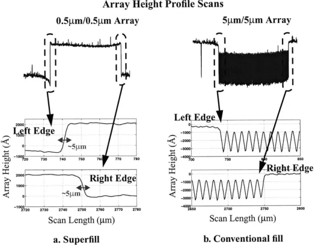
Figure 4.1: Non-Uniform Topography in Copper Electroplating (Superfill) ... 54
Figure 4.2: Test Pattern and Sample Profile Scans for (a) Superfill Plating, and (b) Confor-m al F ill ... . . 5 5 Figure 4.3: Surface Topography Profiles for Pitch Structures (50% Pattern Density): Plat-ing E xperim ent A ... 57
Figure 4.4: Surface Topography Profiles for Density Structures (Varying Pitch): Plating E xperim ent A ... 58
Figure 4.5: Step Height vs. Line Width for Isolated Lines and Array Lines: Plating Exper-im en t A ... . 60
Figure 4.6: Fill Characteristics for Different Trench Widths ... 60
Figure 4.7: Step Height vs. Line Space for Array Lines: Plating Experiment A ... 61
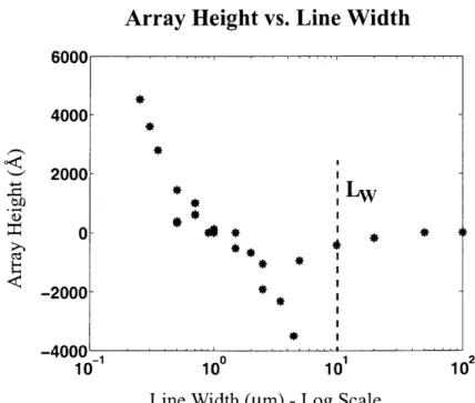
Figure 4.8: Array Height vs. Line Width in Log Scale: Plating Experiment A ... 62
Figure 4.9: Array Height: Bulge and Recess ... 63
Figure 4.10: Array Height vs. Line Space: Plating Experiment A ... 64
Figure 4.11: Sharp Transition from Field to Array Region: Plating Experiment A ... 65
Figure 4.12: Nearest Neighbor Effect in Electroplating: Plating Experiment A ... 66
Figure 4.13: Line Space Effect and Interactions with Line Width: Plating E xperim ent B ... 68
Figure 4.14: Basic Mechanism for Blanket Wafer ... 71
Figure 4.15: Basic Mechanism for Different Trench Width ... 72
Figure 4.16: Basic Mechanism for Different Spacing Width ... 73
Figure 4.17: Diffusion-Adsorption Based Model Proposed by IBM [4] ... 75
Electro-p latin g F ill ... . . 7 6
Figure 4.19: Accelerator-Accumulation: Dependence on Aspect Ratio ... 77
Figure 4.20: Step Height Model Fit vs. Line Width: Plating Experiment A ... 81
Figure 4.21: Array Height Model Fit vs. Line Width: Plating Experiment A ... 83
Figure 4.22: Step Height Model Fit vs. Line Width: Plating Experiment B ... 85
Figure 4.23: Array Height Model Fit vs. Line Width: Plating Experiment B ... 86
Figure 5.1: Example Grid Cell and Cross Sectional View of Plated Profile ... 89
Figure 5.2: Positive and Negative Step Height Cancellation Effect ... 90
Figure 5.3: Example "Random Layout" Grid Cell ... 91
Figure 5.4: Definition of Line Width and Line Length ... 92
Figure 5.5: Example Grid Cell for Binning Calculations ... 95
Figure 5.6: Step Height and Array Height vs. Line Width and Bin Cutoffs ... 96
Figure 5.7: Topography Density vs. Layout Density ... 101
Figure 5.8: Field Thickness Measurement and Data ... 102
Figure 5.9: Initial Copper Profile and Influence on Copper Removal ... 104
Figure 5.10: Surface A rea Calculation ... 105
Figure 5.11: Field T hickness Fit ... 107
Figure 5.12: Chip-Scale Simulation for MIT mask vl.2: A rray H eight and Step H eight ... 109
Figure 5.13: Chip-Scale Simulation for MIT mask vl.2: Field Thickness Variation and Total Thickness Maps ... 110
Figure 5.14: Chip-Scale Simulation for MIT mask vl.2: Layout Density and Topography Density ... 111
Figure 5.15: Prediction and Verification of Chip-Scale Simulation ... 112
Figure 5.16: Sample Profile Scan of Verification Data ... 113
Figure 5.17: Chip-Scale Prediction and Verification: Array Height ... 114
Figure 5.18: Chip-Scale Prediction and Verification: Step Height ... 114
Figure 5.19: Chip-Scale Prediction and Verification: Field Thickness ... 115
Figure 5.20: Chip-Scale Prediction: Final Thickness ... 116
Figure 5.21: Chip-Scale Prediction: Layout Density and Topography Density ... 117
Figure 5.22: Step Height & Array Height Variability from Wafer to Wafer ... 118
Figure 5.23: Field Thickness Variability from Wafer to Wafer ... 120
Figure 6.1: Bulk Copper Polishing: Fine Feature ... 123
Figure 6.2: Bulk Copper Polishing: Large Feature ... 124
Figure 6.3: Bulk Copper Polishing: Large Trench ... 125
Figure 6.4: Initial Surface Heights for Pitch Structures ... 126
Figure 6.5: Initial Surface Heights for Density Structures ... 127
Figure 6.6: Surface Heights for Pitch Structures for Target Field Thickness of 5OOOA 128 Figure 6.7: Surface Heights for Density Structures for Target Field Thickness of 5000A (the spikes are noise in the surface trace) ... 129
Figure 6.8: Copper Clearing and Overpolish: Fine Feature ... 130
Figure 6.9: Copper Overpolish: Fine Feature ... 131
Figure 6.10: Copper Clearing and Overpolish: Large Feature ... 132
Figure 6.11: Copper Overpolish: Large Feature ... 133
Figure 6.13: Array Dishing vs. Overpolish Time ... 135
Figure 6.14: A rray D ishing vs. Pitch ... 136
Figure 6.15: Surface Profiles Showing Dishing and Erosion Trends in the Line/Array Struc-tu re s ... 1 3 9 Figure 6.16: Surface Topography and Copper Thickness Variation vs. Pitch ... 140
Figure 6.17: Erosion for Pad A vs. Features ... 141
Figure 6.18: Erosion for Pad B vs. Features ... 142
Figure 6.19: Array Line Dishing for Pad A vs. Features ... 143
Figure 6.20: Array Line Dishing for Pad B vs. Features ... 143
Figure 6.21: Isolated Line Dishing for Pad A vs. Features ... 144
Figure 6.22: Isolated Line Dishing for Pad B vs. Features ... 144
Figure 6.23: M ask and Test Structure Layout ... 146
Figure 6.24: M ulti-level Process Sequence ... 149
Figure 6.25: Direct Overlap: M1 and M2 Surface Profile and Extracted Cu Thickness 150 Figure 6.26: Half Overlap: M1 and M2 Surface Profile and Extracted Cu Thickness ... 151
Figure 6.27: Dual Overlap: MI and M2 Surface Profile and Extracted Cu Thickness .. 152
Figure 6.28: Direct Overlap: Ml and M2 Surface Profile and Extracted Cu Thickness 153 Figure 6.29: Half Overlap: MI and M2 Surface Profile and Extracted Cu Thickness ... 153
Figure 6.30: Surface Profiles for Half Overlap: Propagation of Ml Dishing to M 2 P ro file ... 154
Figure 6.31: Surface Profiles for Half Overlap: Propagation of M1 Recess to M2 Recess an d D ish in g ... 15 5 Figure 6.32: Contact Mechanics from Yoshida [43] ... 157
Figure 6.33: Stage 1: Rem oval Rate Diagram ... 158
Figure 6.34: Stage 3: Removal Rate Diagram ... 159
Figure 6.35: Sample Electroplated Topography and the Associated "Envelope" ... 159
Figure 6.36: Integrated Implementation of Contact Mechanics and Density-Step Height M o d el ... 16 0 Figure 6.37: CMP Prediction Result of Dishing and Erosion for an Arbitrary Layout .. 161
Figure 6.38: Envelope (Array Height) in Discretized Cells ... 163
Figure 6.39: Integration of Electroplating Model and CMP Model for Complete Chip-Level S im u latio n ... 164
List of Tables
Table 4.1: Example of Line Width and Line Space Transformation... 80
Table 4.2: Step H eight (SH ) Fit ... 81
Table 4.3: A rray H eight (A H ) Fit ... 82
Table 4.4: Array Height (AH) New Model Form (without 1/w term) Fit ... 83
Table 4.5: Process B: Step Height (SH) Fit ... 84
Table 4.6: Process B: Array Height (AH) Fit ... 85
Table 5.1: Example Layout Extraction ... 97
Table 5.2: Assigned Line Width for Each Distribution ... 98
T able 5.3: F ield M odel F it ... 107
Chapter 1
Introduction
With ever-decreasing dimensions and ever-increasing complexity of layout patterns in integrated circuits (IC), semiconductor manufacturing is continually faced with great chal-lenges and difficulties. Over the years, tighter constraints have been imposed on process margins and specifications, and this kind of limitation on process window is projected to be even more severe for later generations of chips [1]. Furthermore, introduction of new materials such as copper and low dielectric constant films for back-end interconnects cre-ates even greater challenges in terms of development of new processes and integration of different materials.
Copper metallization, which has replaced traditional aluminum technology for the state-of-the-art IC's, is expected to have ten levels of metal with as small as 50
A
of copper thickness loss for minimum feature arrays and less than 150A
of wide copper line loss by year 2010. This is a challenging future requirement for the current chemical mechanical polish (CMP) process, especially when current planarization technology often exceeds1000
A
of copper loss in dense regions. The constraint on copper planarization is made more difficult by the incoming topography variation from copper electroplating where large bulge or recess may be present depending on the size of feature arrays, as this incom-ing topography variation is known to impact CMP performance directly by causincom-ing vary-ing removal rates of copper on different pattern regions [2].The Semiconductor Industry Association (SIA) roadmap calls for a full CMP model in near future with 10% topography accuracy of specification limits. Thus, it is critical to have a systematic methodology for the characterization and modeling of pattern dependent issues and problems in both copper electroplating and subsequent CMP processes, and
this is the focus of this thesis work. The research presented here enables rapid and effec-tive development and optimization of each process, and the modeling work for chip-scale topography prediction capability also enables development of relevant layout design rules to limit topography variations.
This chapter is organized into five sections. An overview of copper metallization is given in Section 1.1 with a review of the damascene process used for copper metallization. In Section 1.2, the principles and mechanisms of the electroplating and CMP processes for copper metallization are described. Then, key pattern dependent problems and issues are examined in Section 1.3. Finally, the goal of this thesis is described in Section 1.4, and the thesis organization is given in Section 1.5.
1.1 Introduction to Copper Metallization
Aluminum has enjoyed over three decades usage as the preferred choice of intercon-nect in integrated circuits. However, due to performance and process limitations of alumi-num metallization (e.g. inherent resistivity, electromigration limitations, and increasing challenge to etch very fine aluminum lines), copper metallization has emerged as the lead-ing interconnect technology for deep sub-micron features. Unlike traditional metalliza-tion, where aluminum is deposited on top of inter-level dielectric (ILD), patterned, and etched, copper metallization uses a damascene process. In a damascene process as shown in Figure 1.1, ILD is first deposited and patterned to define "trenches" where the metal lines will lie. Then, a thin layer of barrier material (e.g. tantalum or tantalum nitride with
thickness of around 200 A) is dpsited typically using a physical vapor deposition (PVD)
process on the entire surface to act as a barrier since copper can readily diffuse into silicon and destroy devices. After the deposition of the barrier layer, a copper seed layer (around
using electroplating. Once the patterned trenches and field regions are filled with copper as shown in step 5 in Figure 1.1, the CMP process is used to remove the excess metal outside the desired lines.
1. Oxide 2. Nitride 3. Oxide 4. Barrier 5. Cu Dep. 6. Cu CMP
Dep. and Oxide Pattern/Etch Liner Dep. Dep.
Copper Barrier ILD Si
Layer L. .. 4 Substrate
Figure 1.1: Copper Metallization: Damascene Process
As illustrated above, the copper metallization process involves many integrated pro-cessing steps, and two of the key enabling technologies are copper deposition by electro-plating and copper removal/planarization by CMP. The underlying barrier material must have strong adhesion to the dielectric material and continuos step coverage across deep trenches with good electrical and electromigration performance. Furthermore, the copper seed layer, which is typically deposited by a PVD process, must be also continuous with high step coverage for adequate sidewall and bottom fills, especially for high aspect ratio trenches.
Once a wafer is coated with the copper seed layer, bulk copper is deposited by electro-plating. Many techniques exist for the deposition of copper material on patterned wafers
[3]; however, electroplating, which is the same technology used for printed circuit board
One of the key driving forces for the adoption of electroplating for copper deposition is that this technique enables void-free fills in narrow trenches which is a key requirement for sub-micron feature sizes and high aspect ratios. This void-free fill is often achieved with added chemistries in the copper plating solution so that a higher deposition rate occurs on the bottom of a trench, thus avoiding voids in trenches. Once copper is depos-ited, it must be removed so that copper only remains in the designed trenches. There is no viable solution for plasma etching of copper, and industry has adopted CMP for copper removal and planarization of the damascene structures.
CMP has emerged as the leading planarization technique in silicon integrated circuit fabrication processes and has been extensively applied for planarization requirements of back-end interlayer dielectrics (ILD) as well as for the front-end shallow trench isolation
(STI) process. While other planarization techniques exist, such as spin-on-glass with etch
back or other novel deposition and processing, CMP satisfies both the local and global pla-narity requirements, imposed by lithography depth-of-focus limitations and integration issues for current silicon technologies [5]. In addition, current CMP applications also include polishing of metals such as tungsten [6] and other novel materials which are cur-rently under active research [7, 8]. Finally, CMP has been a key enabler for copper inter-connects; one of the first commercial fabrication processes to use copper is pictured in Figure 1.2 [9].
1.2 Review of Electroplating and CMP: Principles and Mechanisms
We begin with a brief review of the principles and mechanisms in copper electroplat-ing and CMP. In Section 1.3, we then discuss in more detail a key challenge in the pro-cesses related to pattern dependencies. A schematic view of the electroplating tool is shown in Figure 1.3. A wafer surface coated with a thin electrically continuos layer of copper (the seed layer) is immersed in a solution containing copper ions, and the wafer surface is electrically connected to an external power source. Deposition of copper onto the wafer surface occurs by copper ions reacting with electrons to form copper at the wafer surface when current is passed through. The following equation describes the chemical reaction mechanism on the wafer surface which acts as a cathode where cupric ions are reduced to copper atoms.Cu ++ 2e -+ Cu(O) (1.1)
The depleted cupric ions in the solution are replenished by the anode which is another active electrical surface in the electroplating system that completes the electrical circuit. The anode, where an oxidation reaction occurs that balances the current flow in the
sys-tem, is composed of a bulk copper material.
Solid Copper (Anode)
Copper Ion Solution Cu Ions
(plus additive chemicals) Wafer (Cathode)
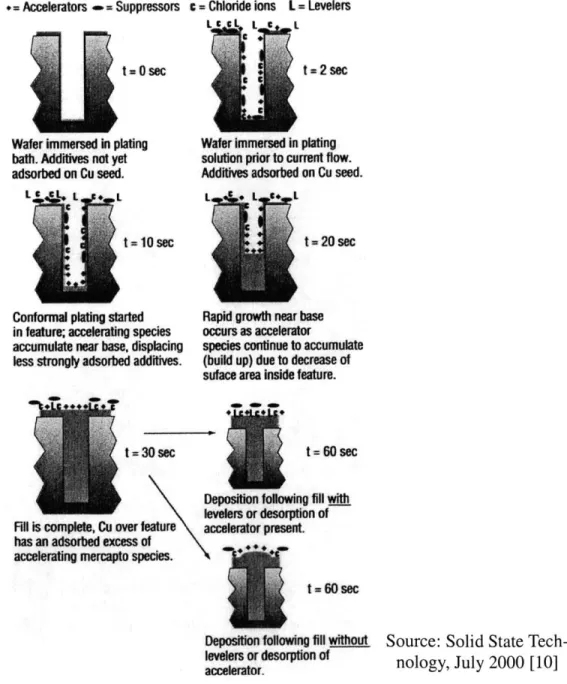
The basic governing principle of deposition is Faraday's law of electrolysis which relates the amount of copper deposited to current density [9]. However, this mechanism is complicated by added chemistry in the copper solution. Typically, these added chemicals are called suppressors and accelerators that are designed to suppress the deposition rate on raised regions while accelerating the deposition rate on the bottom of trenches to achieve void-free fills [10, 11, 12]; such electroplating processes are referred to as bottom-up fill or superfill.
Side View Top View
r
Wafer Slurry Feed
Carrier ar * Holder , SPolishing Pad' Platen-Polishin eed Figure 1.4: CMP Machine
A schematic view of a CMP machine is shown in Figure 1.4. A wafer is held on a
car-rier typically with a back pressure with the surface to be polished facing down towards a polishing pad. A retainer ring on the outer edge of the carrier head prevents the wafer from slipping out of the carrier during polishing. The wafer is then pressed onto a porous poly-urethane polishing pad that is attached to a platen. Both the wafer carrier and the platen are rotated, typically in the same direction with the carrier also having a lapping motion across the pad, and slurry composed of suspended particles in a chemical solution is delivered to
the polishing platform. The removal mechanism has two parts. First, the slurry chemically reacts with the wafer surface film to enhance or inhibit removal of particular materials. Second, mechanical abrasion from the relative movements and pressure of pad and wafer with the slurry particles results in the removal of material [13]. Over time, the pad surface becomes glazed and the removal rate decreases resulting in poor polishing performance. In order to keep the integrity of the pad surface and maintain a reliable polish rate, a con-ditioning head typically with a diamond tip is used to refresh the surface of the pad to maintain the surface characteristics. Other variants of this rotating platform exist such as linear polishing machines, orbital machines, or machines in which the wafer is facing up with a small (smaller than the size of the wafer) polishing pad facing down on a wafer; in all of these tools the basic polishing mechanisms are similar [14].
1.3 Key Problems in Electroplating and CMP
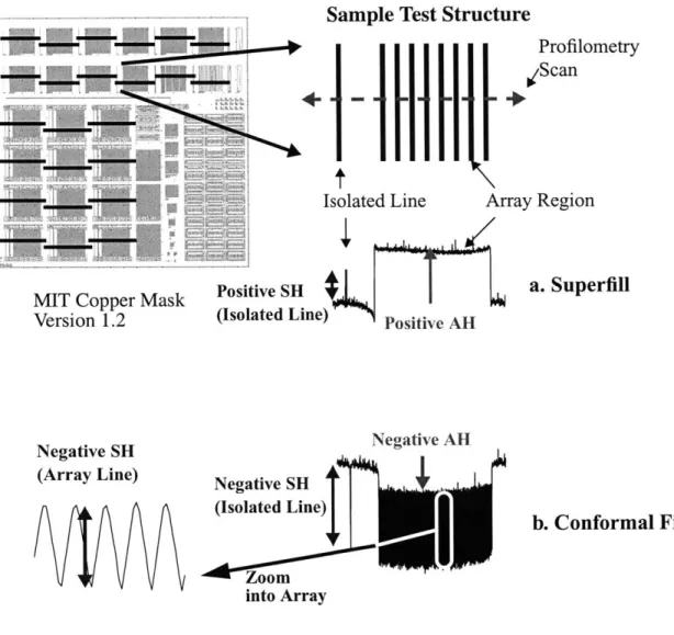
Due to the layout patterns of the underlying trenches to be filled, non-uniform
topogra-phy exists after electroplating. The resulting topogratopogra-phy can be characterized by two
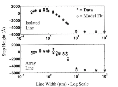
height parameters: a feature scale step height (SH) and an array height (AH) - either recess or bulge - as shown in Figure 1.5 for a superfill electroplating. SH is defined as the height associated with each copper line where copper may stick up or recess depending on the feature size, and the AH is measured from the top of the raised features in an array to the flat copper field region over wide oxide. The magnitude of bulge or recess and step heights are dependent on feature sizes including both line width and space. For large fea-tures, conformal plating is observed, indicating that there is no impact on large features from the added chemistries to cause superfill. However, for fine arrays of lines, copper is filled above the field level nearby, and for large lines with fine spaces, a recess may be present in the copper surface topography. Also, it is possible to have copper sticking up
above a trench when the trenches are narrow and spaces are large. The step and array height trends will be thoroughly examined in Chapter 4.
SH -Step Height
AH AH - Array Height
0 AHA H
Oxide u L
Fine Line Large Line Fine Line Large Line
Fine Space Large Space Large Space Fine Space
Figure 1.5: Non-Uniform Topography in Copper Electroplating (Superfill)
Once a wafer is deposited with copper which exhibits these non-uniform thickness variations, the next step is the CMP process. A copper CMP process is best viewed as hav-ing three intrinsic stages [15]. Stage 1 is the removal of bulk copper on top of a barrier layer, and stage 2 is the removal of the barrier layer. In stage 1, we have homogenous (sin-gle material) polishing where the copper removal rate on different parts of a die is influ-enced by the as-plated initial copper topography created by layout patterns and plating characteristics. For example, Figure 1.6 shows two sample regions: a fine array region and a large pitch region. The fine array region has a bulge and polishes roughly at a blanket copper polish rate. Thus, it achieves a relatively flat surface in that local region later than in the large pitch region where raised features with a 50% pattern density see an acceler-ated copper removal rate compared to the blanket rate. Due to the initial topography, there are differences in removal rates across a die, and thus different parts of a die complete the
removal of excess copper overburden and expose the underlying barrier layer at different polish times. Continued polish beyond barrier removal or overpolish phase is the third
intrinsic stage, where additional differential polish rates occur to due material removal selectivity.
Polished Profile
Oxide U3 U
Fine Line Large Line
Fine Space Large Space
Figure 1.6: Initial Copper Profile and Influence on Copper Removal
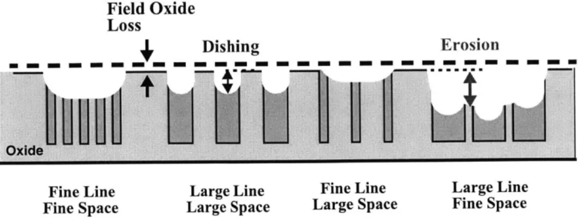
Ideally, the polished copper wafer surface should be perfectly flat; unfortunately, an important non-ideality is that copper lines suffer from dishing and erosion due to CMP. Figure 1.7 shows a cross sectional schematic view of a realistic case suffering from dish-ing and erosion. Dishdish-ing is defined as the recessed height of a copper line compared to the neighboring oxide, erosion is defined as the difference between the neighboring field
region and the post-polish oxide height, and field oxide loss is defined as the difference between the original oxide thickness and the post-polish oxide thickness in wide field area as illustrated.
Field Oxide Loss
+
Dishing ErosionOxide
Fine Line Large Line Fine Line Large Line
Fine Space Large Space Large Space Fine Space
Figure 1.7: Pattern Dependent Problems of Dishing and Erosion In Copper CMP.
These problems of dishing and erosion come from the inherent overpolish stage in copper CMP, and the degree of overpolish depends on two components. First, due to the initial non-uniform topography, there are differences in bulk copper removal rates and thus different regions have different clearing times to the underlying barrier layer. Thus, using the example illustrated above, the region with fine arrays which starts out with a bulge would see a slower clearing time exposing the barrier layer later and thus receive less overpolish. This will result in decreased dishing and erosion for that structure. The second component that adds to the total degree of non-uniformity is the fact that during the barrier
and overpolish, we are again polishing pattern regions created by copper trenches and oxide spacings. Thus, these regions will now again see differences in removal rates of cop-per and oxide and cause added dishing or erosion on top of what is already caused by the differences in clearing time due to the initial copper topography. Thus, the plated
topogra-phy strongly affects CMP performance, and it is important that we develop an integrated
methodology for understanding these pattern dependent issues of both electroplating and
Beyond the non-uniformity problems in single-layer CMP processes, we must also consider multi-level copper metallization and its non-uniform topography and thickness variation. Figure 1.8 illustrates the processing sequence of multi-level copper metalliza-tion in a schematic format (excluding the via layer for the sake of simplicity). (1) After metal 1 polish, there is a certain amount of oxide recess across a structure region. (2) Because of this starting recess on the metal 1 layer, conformally deposited metal 2 oxide has a similar recess shape as the metal 1 recess. (3) The pattern and etch of the uneven oxide makes the bottom of the copper trenches uneven, and the copper deposition profile is also influenced by the uneven profile shape in addition to any non-uniform depositions from electroplating itself. (4) After copper deposition, the wafer is planarized by CMP.
What we are interested in are the metal 2 recess and the remaining line thickness in both an overlap region and non-overlap region, and understanding how these are affected
by the propagation of non-uniform topography created in the lower level. The topography
non-uniformity in the polished metal 2 surface exhibits the similar dishing and erosion problems seen in a single-level polish. However, different degrees of erosion, for example, exist for an uniform array of lines depending on whether a portion of it lies over already-recessed metal 1 region since that region would see higher amounts of recess due to its recessed level even before metal 2 CMP. Another problem in multi-level polishing is that the topography map, often gathered using a surface profiler does not give a complete pic-ture of thickness variation. We have found that electrical measurements of the copper thickness and surface scans are an effective complementary approach to fully characterize multi-level polish behaviors.
Pre-CMP Oxide Profile
Oxide M1 Copper Lines
(1) M1 Polish As Dep. Oxide Profile Oxide
Metal 1
Oxide (2) M2 Oxide DepositionMetal 2
Oxide Oxide (3) M2 Cu Deposition As Dep. M2 Recess Oxide ProfileMetal 2
IMRemaining
Oxide ThicknessMetal 1
Oxide (4) M2 PolishFigure 1.8: Multi-Level Process Sequence
These problems of copper thickness variation due to copper dishing, oxide erosion, and field loss are major challenges in advanced copper metallization processes. Such prob-lems can affect chip performance by introducing variable differences in resistance and capacitance depending on line locations within a chip, and the different amount of dishing and erosion also leads to considerable surface non-planarity with consequent manufactur-ability and process integration difficulties. These problems are seen to largely depend on underlying layout patterns such as pattern density or pattern pitch. Understanding the ini-tial as-plated topography pattern dependencies is a critical first step for modeling of
1.4 Thesis Goals
Copper metallization is becoming a main stream process with tight constraints on thickness variations after CMP. The complexity of copper planarization is increased by the incoming topography variation from copper electroplating where large bulge or recess may be present depending on the underlying features. Thus, it is critical to have a system-atic methodology for the characterization of pattern dependent issues and problems in both copper electroplating and CMP. This characterization methodology must also be cou-pled to a model that captures these pattern effects for prediction of plating and CMP results for arbitrary product patterns.
The basis of the methodology includes identifying key layout and process parameters that cause variations in electroplated step heights and CMP dishing/erosion. The identifi-cation of the key pattern dependent factor is possible by design of test structures that con-sist of various pattern factors combining a wide range of line widths and spaces. The design of the test structures is also closely tied with measurement and analysis techniques so that we can effectively capture these dependencies.
Using the same test mask as the vehicle of characterization for both electroplating and CMP, we can study and understand pattern dependent behaviors in each process and fur-thermore understand how the electroplated topography affects the CMP process. As described earlier, different array heights are possible for an electroplated die depending on the size of features and spacings, and thickness variations of dishing and erosion are present after CMP due to layout patterns. Based on the trends of these non-uniformities, a pattern dependent model can be formulated. With characterization and model formulation, one can understand the fundamental limitations of these thickness variations for a specific process.
In addition to experimentally inducing and characterizing pattern dependent thickness variations, a model is needed capable of predicting thickness variations across an entire chip by relating layout parameters such as pattern density and line width with calibrated model coefficients. Thus, a layout parameter extraction algorithm needs to be developed so that an extracted layout result can be efficiently used with the model in predicting chip-level variations. Furthermore, when chip-scale prediction is possible based on layout parameters, relevant layout design rules can be generated to limit thickness variations after the copper electroplating and CMP process.
In summary, the main goals and objectives of this thesis are as follows:
1. Develop test structures and masks to explore key pattern effects in both
electroplat-ing and CMP processes.
2. Characterize pattern dependent problems in electroplating as a function of underly-ing pattern features and develop a model to capture the variation.
3. Develop layout parameter extraction procedures and apply the electroplating model
in chip-scale simulation and prediction for arbitrary layouts.
4. Characterize both single level and multi-level CMP pattern dependent effects as a function of underlying pattern features.
5. Illustrate the integration of electroplating topography prediction and CMP modeling for predictive chip-scale simulation of final interconnect topography.
1.5 Thesis Organization
This thesis is organized into seven chapters. Chapter 2 outlines the overall methodol-ogy for both electroplating and CMP characterization and modeling and highlights differ-ent parts of the overall method with an emphasis on how they integrate to form a coherdiffer-ent methodology for characterizing and modeling interconnect topography.
Once the overall methodology is presented, the subsequent chapters discuss in detail each part of the methodology. Chapter 3 covers the test structure and mask design which is
the key first step in experimentally exploring pattern dependencies in a process. Design issues and structure descriptions are presented for a single-level mask. Then, a multi-level mask description is given to study polishing effects in multi-level interconnect processes. In Chapter 4, electroplating characterization is presented and followed by modeling of electroplated non-uniform surface topography. Trends are observed and various proposed physical and superfill mechanisms are examined to formulate model variables. Then, Chapter 5 describes layout parameter extraction and chip-scale simulation using the devel-oped model, and a chip-scale plating prediction result is presented.
Understanding of pattern dependent electroplating non-uniformity is essential for the subsequent CMP process since the initial topography directly impacts the planarization of the CMP process. In Chapter 6, CMP characterization is presented for both single-level and multi-level pattern dependencies. The use of electrical test structures and their analy-sis are also presented. The ability to gather electrical data, especially for fine lines which are often hard to measure with surface profile tools, is shown to complement surface height measurement. Then, an overview of the pattern dependent CMP model is described followed by the integration of the electroplated topography simulation result and a CMP chip-scale model. Finally, Chapter 7 summarizes the key results and contributions of this thesis and concludes with directions for future research in this area.
Chapter 2
Comprehensive Characterization and Modeling
Methodology
Characterization of the pattern dependent non-uniformities in copper electroplating and CMP is needed to understand the fundamental limitations of each process and assist in new process development efforts. For the characterization work to be meaningful and valid, it must be carried out in a systematic and methodical way. This chapter first gives an overall methodology to characterize an electroplating process to understand the plated thickness variations such as step height and array height. The development and application of a pattern dependent electroplating model coupled to the characterization method is pre-sented with an overall goal of chip-scale thickness simulations for any random layouts. Then, a similar methodology is illustrated for the characterization and modeling of the CMP process, with an emphasis on the integration of electroplating and CMP simulations. This chapter is intended to give an overall picture of all the pieces involved in the charac-terization and modeling work to illustrate how they are interrelated, and the subsequent chapters give details of each individual part of the methodology.
2.1 Electroplating Characterization and Modeling
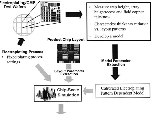
The overall methodology for electroplating characterization and modeling is summa-rized in Figure 2.1. To characterize as-plated copper topography variation for a particular electroplating process, a wafer patterned with a dedicated test mask is processed. The test mask consists of various combinations of line widths and line spaces to cover a wide range of pattern densities and features. The designed test patterns are used with measurement and analysis techniques to capture and identify key layout dependencies in the plating
pro-cess. Once a wafer is electroplated, step height and array bulge or recess are measured across many test pattern arrays and isolated features using a surface profiler. Also, field areas (e.g. large region without any copper lines) are measured for the absolute copper thickness so that we can translate relative surface height measurements into absolute thickness throughout the chip. The direct measurement of copper film thickness has become possible due to emerging tools such as the Metapulse system by Rudolph Tech-nologies, or the Impulse 300 system by Philips Analytical.
Electroplating/CMP p
Test Wafers
H
Product Chip Layou Electroplating Process
- Fixed plating process settings
t
Layout Parameter Extraction
- Measure step height, array bulge/recess and field copper
thickness
- Characterize thickness variation vs. layout patterns - Develop a model
I
Model Parameter Extractioni
Chip-Scale Calibrated Electroplating
Simulation Pattern Dependent Model
Prediction of Step Height and Array Height Across a Chip
Figure 2.1: Overall Methodology for Characterization and Modeling of
The measured data is analyzed to assess and identify key pattern dependencies, and their trends are examined as a function of specific layout features. This characterization serves as a powerful tool to understand the plating behavior and can help an engineer to identify and resolve any non-uniformity issues before they cause any difficulties in manu-facturing or create yield problems. Once a process is fully characterized for its pattern induced thickness profiles, a semi-empirical model is developed incorporating the macro-physics of electroplating; this model captures the key pattern effects as a function of underlying layout patterns. The model can be calibrated for different electroplating reci-pes.
The model parameters are then extracted, and the calibrated electroplating pattern dependent model can be used to perform chip-scale simulations for the thickness variation for other chips fabricated using the calibrated electroplating process. The chip-scale simu-lation can be done for any arbitrary layout; to accomplish this, the relevant layout parame-ters must be extracted before the simulation can be performed. The result of the simulation is step height and array height across an entire chip for the given electroplating process. The simulation result can be used to determine overall non-uniformity as well as to check for any regions on the chip with excess copper bulge or recess. Furthermore, the model-based simulation can be used to develop intelligent design rules for layout patterns: for example, once any possible trouble spots are determined, the layout can be modified to alleviate the problem by inserting dummy fills to equalize the pattern effects.
Detailed descriptions for each part of the methodology, including the test mask design, non-uniformity characterization and model development, chip-scale simulation and pre-diction, are presented in Chapters 3, 4, and 5, respectively.
2.2
CMP Characterization and Modeling
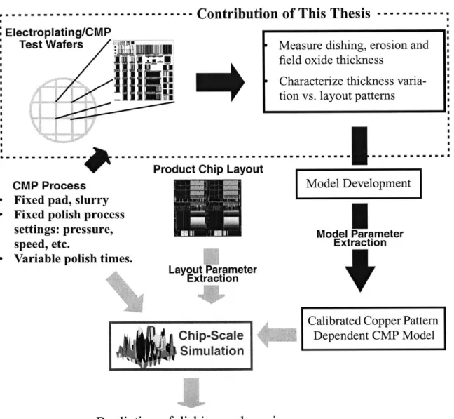
Characterization and modeling of pattern dependent variations of copper dishing and oxide erosion for CMP process is shown in Figure 2.2 and has similar flow as the method used for electroplating. A patterned wafer deposited with copper is polished using a partic-ular process. Then, dishing of copper lines are measured for isolated lines and array lines, and erosion of oxide is measured for array lines using a surface profiler. In addition to these surface measurements, optical field area measurements of dielectric thickness are done to obtain the absolute remaining film thicknesses at various locations such as at either ends of each surface trace. Also, electrical measurements are performed to gather line resistance, which are later converted to copper thickness for comparisons with the sur-face profile data and optical dielectric film thickness. This electrical data analysis has been found to be particularly useful for multi-level CMP characterization where surface profile scan does not necessarily indicate the remaining copper thickness profile. It has been found that the use of both surface profiles and electrical measurements is necessary to get a complete picture of the polished thickness/surface variations. All of these measurements are done across various pattern regions to ensure that we have a data set that covers wide range of pattern features.
Based on the characterization of the pattern effects and incorporating polishing funda-mentals such as blanket removal rates and material removal selectivities, a semi-empirical pattern dependent CMP model is developed. The calibrated copper CMP model can be used for chip-level simulation of any arbitrary layout (e.g. a product chip) using relevant layout parameters extracted from the layout. The chip-scale simulation gives prediction of dishing and erosion and can be used for layout design rules such as assessing the effective-ness of dummyfication. This thesis is not to cover all aspects of this methodology to understand and model CMP variations. Rather, this thesis focuses on the development of
the test mask that serves as the foundation for all characterization and modeling work. Then, the thesis presents characterization methodology and result for single layer and multi-layer CMP thickness variations. The modeling and simulation aspects of the meth-odology are developed by a research colleague, Tamba Tugbawa. Please refer to his Ph.D thesis for the complete description of the modeling work for CMP [16].
...-.-..-.- . .--- Contribution of This Thesis
---Electroplating/CMP
Test Wafers Measure dishing, erosion and
field oxide thickness
Characterize thickness varia-tion vs. layout patterns
Product Chip Layout CMP Process
- Fixed pad, slurry - Fixed polish process
settings: pressure, speed, etc.
- Variable polish times.
Layout Parameter Extraction
Model Development
Model Parameter Extraction
Calibrated Copper Pattern
Chip-Scale Dependent CMP Model
Simulation
Prediction of dishing and erosion
Figure 2.2: Overall Methodology for Characterization and Modeling of
2.3 Overview of Integration for Electroplating and CMP Chip-Scale
Simulations
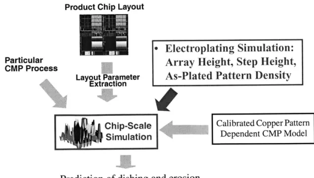
As discussed in Chapter 1, the initial non-uniform topography has a directly impact on the CMP polishing behavior and this topography is created by the pattern dependency in copper deposition in electroplating. Thus, we need to define what topography information is transferred to CMP model so that it can make an effective use of the plating information. The plating topography information needed by CMP is dictated by CMP simulation needs as the calibrated CMP model uses the electroplated topography as the initial condition of the die surface. Specifically, CMP uses the electroplated topography information of final thickness, step height, and as-plated pattern density to calculate removal rates at various locations across a whole chip in bulk copper removal stage. Subsequently, CMP model uses extracted layout parameters of a chip to predict copper dishing and erosion in the third stage of polishing. Figure 2.3 summarizes how the electroplated topography informa-tion is fed-forward to the CMP modeling methodology.
Product Chip Layout
Particular CMP Process
. Electroplating Simulation:
Array Height, Step Height,
Layout ParameterAs-Plated Pattern Density
Extraction
Chip-Scale Calibrated Copper Pattern
Simulation Dependent CMP Model
Prediction of dishing and erosion
Figure 2.3: Integration of Electroplating Model and CMP Model for Complete Chip-Level Simulation
How the electroplated topography is used in the CMP model is summarized in Chapter 6. As it can be seen, each characterization and modeling methodology for electro-plating and CMP does not change for the purpose of the integrating the two models for chip level simulation. The integration is efficiently done through three electroplated topog-raphy information, array height, step height, final thickness, and pattern density, that are fed-forward to the CMP simulation. This information transfer is done for each discrete unit of grid cells where the grid cells are common in both electroplating and CMP simula-tions. Thus, all information from electroplating can serve as an input to the CMP model as
Chapter 3
Test Structure and Mask Design
The key underlying vehicle that enables characterization and modeling of copper inter-connect pattern dependency is a test mask. In this chapter, we present descriptions of test structures for a single level test mask. Measurement requirements and issues are also illus-trated. The test mask described here has evolved from the original copper CMP test mask version 1.0 [17] through many experimental studies and subsequent enhancements of mask designs.
The test mask can be used for rapid characterization of electroplating and CMP char-acteristics such as consumable/tool comparisons, and process dependencies. Furthermore, these test masks can serve as a vehicle for calibrating and validating physical or semi-empirical models. There exist many process and integration issues in copper metallization, some of which are void-free electroplating especially for high aspect ratio trenches, barrier reliability, and CMP endpoint controls. However, the test masks presented in this thesis, including the multi-level mask design presented in Appendix B, are specifically designed to target layout pattern dependent behavior and related studies for copper electroplating and subsequent CMP planarization.
This chapter is organized as follows. First, structure design issues and principles are described including the relevant characteristic length scales in electroplating and CMP processes. Then, a single level mask is described followed by measurement descriptions.
3.1 Structure Design Philosophy and Issues
The fundamental issue in designing a test mask is understanding what kinds of pat-terns do actually matter in causing non-uniform topography after processing. Having a
wide range of patterns does not necessarily mean that the key pattern problems can be identified. A test reticle should contain relevant pattern factors, such as pattern density, that a process of interest has dependency on. Identifying these pattern factors typically occurs through previous studies or results in similar processes; for example, studies of tungsten CMP process pattern effects can help in assessing the copper process since they are both in-laid processes. In addition to the types of patterns, it is also critical that the designed patterns have a structure size that accounts for a characteristic length of a process so that each structure or pattern does not get confounded pattern effects from neighboring structures.
For example, if a structure region is only 500 gm wide when a characteristic length is
5 mm for a particular process, then the pattern effect from this particular structure has a significant amount of confounded influence from surrounding regions, complicating anal-ysis especially when understanding of pattern interactions is not clear. Thus, each struc-ture size should be big enough to attain a uniform local pattern environment. In addition, a structure design needs to remain simple, as complicated designs often cause measurement and analysis difficulties.
The placement of each pattern structure on the mask, also known as floorplanning, is the next critical factor in a test mask design. Floorplanning offers designers the flexibility of being able to place structures in strategic locations to either minimize or to cause possi-ble structure to structure interactions. For instance, we have found that a field area of at least 100-200 pm is needed between structures for each structure to be considered "iso-lated" from other structures in the overpolish phase of the copper CMP process [18]. The designed structures and their placements must also offer strategic and easy measurement plans for efficient and effective data gathering. For example, if a structure size is too big or if two structures are side by side, then a surface profile scan would contain excess noise
from leveling by the profiler or distortions from wafer warp that would make it hard to dis-tinguish what is noise and what is actual behavior. We encountered this measurement diffi-culty due to having structures side by side in an early test mask design (version 1.0), and all the subsequent designs have eliminated the problem by inserting field area separations between structures.
All of the issues described above - pattern factors, structure size, and placement - are critical in a test mask design to capture key pattern effects in a process. These design
issues are described in detail in test structure designs in the following sections.
3.1.1 Characteristic Length Scales in Electroplating and CMP
As discussed in the previous section, structure design must take into account charac-teristic length scales in a process. This section thus summarizes key length scales observed in the electroplating and CMP processes so that structure design principles are better understood. Since we want to use the same test mask to characterize both electroplating and CMP, the design must meet the characteristic length scales for both processes. This section first summarizes the relevant length scales in electroplating. Design of test struc-tures is a iterative process where findings from experiments enable improvements in design. Thus, in discussing electroplating and CMP length considerations, we refer to early studies and experimental results; in may cases these results are presented later in more detail for electroplating in Chapter 4, and for CMP in Chapter 6.
In the electroplating process, our studies have found that the plated profile depends primarily on the details of the local feature itself. To first order, electroplating is a local-ized process where the plating depends on the line and its surroundings including the spac-ing and the nearest neighbors [19]. Thus, the characteristic length scale is equal to the feature size including the nearest neighbors within 2-5 ptm of the feature. Thus, if there are
more than several lines in a test structure, a uniform and self-contained local pattern envi-ronment is formed. Also, it is observed that if a line is positioned away from other lines by more than 5-10 tm, then the line can be considered as an isolated line where it is not influ-enced by other lines.
The test mask design described later has a line/array structure with an isolated line that is hundreds of microns away from other structures, and this is far greater than the 3-5 p.im transition region length scale seen in electroplating. Thus the line structure can be effec-tively treated as an isolated line. For an array region consisting of sequences of lines and spaces, the test structure size is on the order or millimeters containing regular arrays of many lines. Thus the array size of the array region is large enough for use of the structures in studies of pattern effects in electroplating. We find that the constraining characteristic length scale governing the test mask design is imposed by the CMP process, rather than by the electroplating process. Thus, the designed test structures can be used effectively for an integrated studies of pattern effects in both processes if they satisfy the more difficult CMP imposed design challenges.
In oxide CMP, one length scale has been found to dominate: a "planarization length" on the order of 3-7 mm effectively averages the density of raised topography within that range, determining the relative rates of polish [20]. In copper polishing, on the other hand, three different length scales appear to be at work. First, an analogous long-range (e.g.
6 mm in [21]) pattern density dependence appears to be important during the initial
pla-narization of the bulk copper. Second, a relatively sharp and short range transition of approximately 50-200 pim is observed between a field oxide region and the dishing/ero-sion profile in an array region as shown in Figure 3.1, or between two different density/ pitch array regions [18, 22]. We have also found that field area of at least 100-200 pim is needed between structures for each structure to be considered "isolated' from other
struc-tures in the overpolish phase of copper CMP process [18]. Finally, very short range depen-dencies on the order of the individual line width or space (feature length scale) can substantially accelerate or limit dishing and erosion [22].
0 -200 -400 -600 -800 1000 1500 2000 2500
Figure 3.1: Sample Erosion Profile Across an Array Region
The variety of these length scales and their influences must be accounted for in the design and layout of test structures for copper interconnect pattern dependency character-ization, as well as in the measurement and analysis of topography data.
3.1.2 Basic Test Structure Design: Line/Array
In this section we first describe the basic line/array structure used to explore array and step height in electroplating fill, and dishing and erosion in the CMP process. We then dis-cuss the key principles and guidelines for structure design and layout to address the length scales discussed above, as well as how these structures support physical and electrical measurement of key pattern dependencies.
50,-200pm tran-ition
ield ield