Publisher’s version / Version de l'éditeur:
The Journal of Physical Chemistry B: Condensed Phase, 107, 51, pp.
14326-14335, 2003-12-25
READ THESE TERMS AND CONDITIONS CAREFULLY BEFORE USING THIS WEBSITE. https://nrc-publications.canada.ca/eng/copyright
Vous avez des questions? Nous pouvons vous aider. Pour communiquer directement avec un auteur, consultez la première page de la revue dans laquelle son article a été publié afin de trouver ses coordonnées. Si vous n’arrivez pas à les repérer, communiquez avec nous à PublicationsArchive-ArchivesPublications@nrc-cnrc.gc.ca.
Questions? Contact the NRC Publications Archive team at
PublicationsArchive-ArchivesPublications@nrc-cnrc.gc.ca. If you wish to email the authors directly, please see the first page of the publication for their contact information.
NRC Publications Archive
Archives des publications du CNRC
This publication could be one of several versions: author’s original, accepted manuscript or the publisher’s version. / La version de cette publication peut être l’une des suivantes : la version prépublication de l’auteur, la version acceptée du manuscrit ou la version de l’éditeur.
For the publisher’s version, please access the DOI link below./ Pour consulter la version de l’éditeur, utilisez le lien DOI ci-dessous.
https://doi.org/10.1021/jp035699k
Access and use of this website and the material on it are subject to the Terms and Conditions set forth at
Photoelectrochemical generation of electronically conducting
polymer-based hybrid junctions on modified Si(111) surfaces
Fabre, Bruno; Lopinski, Gregory P.; Wayner, Danial D. M.
https://publications-cnrc.canada.ca/fra/droits
L’accès à ce site Web et l’utilisation de son contenu sont assujettis aux conditions présentées dans le site LISEZ CES CONDITIONS ATTENTIVEMENT AVANT D’UTILISER CE SITE WEB.
NRC Publications Record / Notice d'Archives des publications de CNRC:
https://nrc-publications.canada.ca/eng/view/object/?id=b0d0d3ef-f5a7-4f33-9baa-56285c529743 https://publications-cnrc.canada.ca/fra/voir/objet/?id=b0d0d3ef-f5a7-4f33-9baa-56285c529743Photoelectrochemical Generation of Electronically Conducting Polymer-Based Hybrid
Junctions on Modified Si(111) Surfaces
Bruno Fabre,†Gregory P. Lopinski, and Danial D. M. Wayner* Steacie Institute for Molecular Sciences, National Research Council of Canada, Ottawa, Ontario K1A 0R6, Canada
ReceiVed: June 16, 2003; In Final Form: October 15, 2003
The modification of Si(111) surfaces with Si-C linked alkyl monolayers terminated by electrochemically polymerizable di(2-thienyl)carbinol moieties has been investigated by different spectroscopic techniques including IR spectroscopy, X-ray photoelectron spectroscopy (XPS), and high-resolution electron energy loss spectroscopy (HREELS). These surfaces were prepared from the photochemical reaction of ethyl undecylenate with hydrogen-terminated Si(111), followed by the conversion of the produced terminal ester groups into the tertiary alcohol using 2-thienyllithium. Despite the steric constraints induced by the aromatic rings in the monolayer, the absolute surface coverage of the organic chains was found to be high, ca. 40%. Differential capacitance measurements revealed that the derivatization procedure introduced surface states probably due to some oxidation of the Si(111) surface occurring during the photochemical step. The photopotentiodynamical oxidation of the modified Si(111) surfaces in the presence of thiophene yielded strongly adherent and smooth conducting polythiophene films. These photoelectrogenerated hybrid polythiophene-silicon junctions were then characterized by ex situ electrical measurements (dc transport, ac impedance, and surface potential measurements). The expected diode behavior due to the formation of a Schottky barrier at the alkyl/Si(111) interface was clearly observed although the rectification was rather weak and the characteristics highly nonideal. The surface states at the silicon interface were found to play a major role in determining the electrical properties of such junctions.
I. Introduction
The covalent attachment of organic monolayers to semi-conductor surfaces is of growing interest for potential applica-tions from surface passivation to the incorporation of chemical/ biochemical functionality at interfaces for use in molecular electronics, photovoltaic devices, and chemical/biological sens-ing.1Among the various approaches, reactions of
hydrogen-terminated silicon surfaces, Si(111)-H, have been demonstrated to be one of the most versatile to yield robust monolayers showing considerable chemical stability.2-7Although many of
the organic films produced by this route were terminated by unreactive methyl groups,2,3a,c,d,4b,f,5a,7b,cother much more
reac-tive terminal groups also have been introduced, such as acids or esters,4a,d,g,5a,7bamines,4a,5c,7aalcohols,4a,5a,baromatic rings,6
and redox centers,3b,7e which were used for the subsequent
attachment of more complex organic or bioorganic structures. Unlike organothiol monolayers assembled on gold,8,9it should
be possible to tune the electrical properties of such hybrid molecule/silicon architectures by varying the dopant type (p or n) or density, and the illumination level of silicon. Moreover, these films are expected to exhibit a greater thermodynamic stability if one compares the bond energies of Si-C (369 kJ mol-1) and Si-O (368 kJ mol-1)10with that of Au-S (∼190
kJ mol-1).11
Recently, Laibinis12 and ourselves13 derivatized Si(111)
surfaces with Si-C linked alkyl monolayers terminated by
electrochemically polymerizable moieties, namely pyrrole12and
thiophene.13The photoelectrochemical oxidation of such
modi-fied electrodes in the presence of the monomer in solution yielded conducting organic polymer films covalently bound to silicon, which exhibited morphological and adherence charac-teristics better than those of the same polymers electrodeposited on unmodified silicon. A major advantage of this approach is that it does not require nor produce a silicon oxide layer that would serve as an additional insulating barrier. Moreover, as the electropolymerization process requires the irradiation of silicon, the covalent attachment of the organic monolayer reduces the number of available surface sites where recombina-tion of generated electrons and holes can take place. In this respect, it has been reported that silicon surfaces modified with alkyl monolayers can be produced with electrically active defect densities of less than one per 50000 surface atoms,14comparable
to the defect densities for device quality SiO2/Si interfaces. Thus,
holes can tunnel from the silicon surface to the terminal monomer units through the alkyl chains and promote the oxidation of the monomer present in solution. Indeed, for covalently attached molecules, hole tunneling through σ-bonded alkyl chains has been found to be more efficient than electron tunneling.15 In fact, the values of the structure-dependent
attenuation factor β16,17suggest that this process is as efficient
as electron tunneling through π-conjugated systems. In contrast, the presence of a silicon oxide layer between the silicon surface and the alkyl chain would inhibit hole tunneling.
The fabrication of junctions incorporating a doped conjugated polymer, such as polythiophene, offers a number of other potential advantages. Compared to metal-organic-semiconductor (or metal) junctions for which an evaporated metal (e.g., Au or Al) is typically used for the electrical top contact, the use of a
* Corresponding author. Fax: 1 613 990 4200, Tel: 1 613 991 0940, E-mail: dan.wayner@nrc.ca.
†Permanent address: Laboratoire d'Electrochimie Mole´culaire et Mac-romole´culaire (Synthe`se et Electrosynthe`se Organique - Unite´ Mixte de Recherche No. 6510 associe´e au CNRS), Universite´ de Rennes 1, Campus de Beaulieu, 35042 Rennes Cedex, France.
14326 J. Phys. Chem. B 2003, 107,14326-14335
10.1021/jp035699k CCC: $25.00 © 2003 American Chemical Society Published on Web 11/25/2003
conducting polymer as the top contact could be particularly attractive,18avoiding potential damage to and/or penetration into
the organic layer that often results from metal deposition.19,20
Moreover, unlike a metal, the conductivity of these materials can be tuned over a large range either by electrochemical doping or to a lesser extent by the nature of the compensating anion. We present herein a detailed characterization of the thiophene-terminated alkyl monolayers bound to silicon and the photo-electrochemical grafting of polythiophene on such modified surfaces. Various experimental techniques including IR spec-troscopy, contact angle goniometry, ellipsometry, X-ray pho-toelectron spectroscopy (XPS), high-resolution electron energy loss spectroscopy (HREELS), and electrochemistry (cyclic voltammetry and differential capacitance measurements) have been used. The positive effects of the presence of the surface-confined monomer units on the electropolymerization process as well as on the morphological characteristics of the resulting conducting films are also discussed. To evaluate the potential of the polythiophene/alkyl/Si(111) junctions for use in hybrid silicon/organic devices we have also carried out ex situ electrical characterization including dc transport, ac impedance, and surface potential measurements. The structures fabricated here exhibit properties expected for MIS (metal-insulator-semi-conductor) systems.
II. Experimental Section
Preparation of Thiophene-terminated Monolayers. The organic derivatization of silicon by thiophene-terminated mono-layers is depicted in Scheme 1.
A single side polished silicon(111) shard (1-5 Ω cm, n-type, phosphorus doped, thickness ) 250 ( 25 µm, Virginia Semiconductor Inc.) was cleaned in 3:1 v/v concentrated H2
-SO4/30% H2O2 at 100 °C for 30 min, followed by copious
rinsing with Milli-Q water.
Caution!The concentrated H2SO4:H2O2(aq) piranha solution
is Very dangerous, particularly in contact with organic materi-als, and should be handled extremely carefully.
The surface was etched with ppb grade 40% aqueous argon-deaerated NH4F (Olin) for 20 min to obtain atomically flat
Si-(111)-H.2eIt was then dipped in argon-deaerated Milli-Q water
for several seconds, dried under a nitrogen stream, and transferred into a Pyrex Schlenk tube containing ca. 15 mL of deoxygenated ethyl undecylenate (Aldrich, 97%). The solution was thoroughly purged with argon for 30 min, the Schlenk tube was sealed with paraffin film (Parafilm M), and the solution was irradiated for 3 h in a Rayonet photochemical reactor (300 nm). The ester-modified surface (Si(111)-C10H20COOC2H5
denoted as 1) was then rinsed copiously with THF and 1,1,1-trichloroethane, sonicated for 10-15 min in CH2Cl2, and dried
under a nitrogen stream.
The terminal ester groups were converted into di(2-thienyl)-carbinol moieties by reaction with 2-thienyllithium (1 M in anhydrous THF, Aldrich). After 4 h at room temperature under argon, the solution was heated to 65-70 °C and kept at this
value overnight. The solution was allowed to cool to room temperature and the thiophene-modified surface was rinsed with 1% v/v CF3COOH/THF, Milli-Q water, THF, and TCE,
sonicated in CH2Cl2for 10-15 min, and dried under a nitrogen
stream.
Surface Characterization.Fourier transform infrared (FTIR) measurements were recorded using Si(111) attenuated total reflectance (ATR) crystals (25 × 4.5 × 1 mm3, Harrick
Scientific Corp.) using a Nicolet MAGNA-IR 860 spectrometer at 4 cm-1resolution. The sample compartment was purged with
dry nitrogen. High-resolution electron energy loss spectroscopy (HREELS) was carried out under ultrahigh vacuum conditions with a LK3000 (LK Technologies) spectrometer. For the present experiments the nominal system resolution was set to 36 cm-1.
This resulted in elastic peak intensities ranging from ∼5 × 10⁵
to 2 × 10⁴counts per second (for incident energies from 3 to
20 eV) with a fwhm of ∼60 cm-1.
The thickness of the organic monolayers was estimated using a Gaertner model L116S ellipsometer with a HeNe laser and an angle of incidence of 70°. n ) 1.46 was used as the refractive index of the monolayer, and n ) 3.85 and k ) 0.02 were used for the silicon substrate. Water contact angles were measured with a Tantek goniometer supplied by Cole-Parmer under ambient conditions using a columniated horizontal light beam to illuminate the liquid droplet.
XPS measurements were performed using a PHI 5500 system with monochromatic Al KR1photons at 45°incidence and 45°
takeoff angle. Spectra were fitted with Gaussian profiles using standard procedures. Sensitivity factors of 0.733 (O 1s), 0.314 (C 1s), 0.368 (Si 2p), 0.717 (S 2p), and 0.426 (S 2s) were applied. All peak positions were normalized to the C 1s peak of adventitious carbon which was assumed to have a binding energy of 285.0 eV.
AFM images were recorded with a Nanoscope IIIa from Digital Instruments using silicon (tapping mode) or silicon nitride (contact mode) sharpened tips. They were taken in ambient air and flattened.
Electrochemical Characterizations.The cyclic voltammetry and differential capacitance measurements were performed with an Autolab electrochemical analyzer (PGSTAT 30 potentiostat/ galvanostat from Eco Chemie B.V., equipped with the GPES/ FRA software) in a self-designed three-electrode Teflon cell. The working electrode, unmodified or modified Si(111) (elec-trochemically active area ∼0.68 cm2), was pressed against an
opening in the cell bottom using an O-ring seal. An ohmic contact was made on the previously polished rear side of the sample by applying a drop of an In-Ga eutectic (Alfa-Aesar, 99.99%). The counter electrode was a platinum foil and all potentials were relative to the system 10-2 M Ag+|Ag in
acetonitrile (+0.29 V vs aqueous SCE). The differential capacitance measurements were analyzed only in the frequency range (typically 50 kHz to 500 Hz) in which the phase angle of the complex impedance was greater than 80°, i.e., the range for which the system behaved primarily as a combination of capacitive circuit elements. The differential capacitance mea-surements were performed in the dark.
Tetra-n-butylammonium perchlorate Bu4NClO4and
tetra-n-butylammonium hexafluorophosphate Bu4NPF6were purchased
from Fluka (puriss, electrochemical grade). Acetonitrile (Merck) was freshly distilled over calcium hydride prior to use. The electrolytic medium was dried over activated, neutral alumina (Aldrich) for 30 min, under stirring and under argon. About 30 mL of this solution was transferred with a syringe into the electrochemical cell.
The electropolymerization experiments were carried out under illumination after the addition of thiophene at 5 × 10⁻² M
SCHEME 1: Derivatization of Si(111) Surfaces with Thiophene-Terminated Alkyl Monolayers
(Aldrich, 99+%), previously distilled under vacuum and stored over alumina, into the electrolytic solution. The samples were illuminated by an optical fiber (Fiber Lite, Model 190) having light intensities in the range of 65-130 mW. All electrochemical measurements were carried out inside a homemade Faraday cage, at room temperature (20 ( 2 °C) and under a constant flow of argon.
Electrical Characterizations of Polythiophene-Alkyl-Si(111) Junctions. Ex situ electrical measurements on the polythiophene/alkyl/Si(111) junctions were carried out using a probe station (Cascade Microtech) equipped for temperature-dependent measurements in the 20-200 °C range. Current-voltage characteristics were acquired with a Keithley 2400 source meter whereas the aforementioned Autolab electrochemi-cal analyzer was employed for ac impedance measurements. To minimize series resistance effects on the electrical charac-teristics of the junctions the back of the silicon wafer was etched by a drop of 2% HF and coated with InGa eutectic. Surface potential measurements were carried out with a Kelvin probe (KP Technologies), using the white light fiber optic source described above to determine the photovoltage.
III. Results and Discussion
Film Thickness and Surface Wetting Properties of the Functionalized Monolayers on Si(111).The thickness of the freshly prepared thiophene-terminated alkyl monolayer (Si(111)-C10H20C(2-thienyl)2OH denoted as 2) estimated by ellipsometry
is 20 ( 1 Å, 4 Å greater than the value determined for the ester-terminated monolayer (16 ( 1 Å). Contact angle measure-ments performed with water indicate that the thiophene-modified surface is slightly less hydrophobic than the ester-modified surface, 67 ( 2°and 72 ( 2°respectively. Such a decrease is consistent with the presence of hydroxyl in the terminal groups, which would counterbalance the hydrophobicity of the aromatic rings. Nevertheless, as judged by the IR data (discussed below), a less ordered structure also could account for this result.
Spectroscopic Characterization.The positions of the prin-cipal vibration bands observed in the infrared spectra of ester-and thiophene-terminated alkyl monolayers are shown in Table 1.
For 1, the antisymmetric (νas(CH2)) and symmetric (νs(CH2))
methylene stretching modes appear at 2921 and 2851 cm-1,
respectively, which is therefore indicative of a reasonably densely packed, monolayer with some gauche defects,21 as
already demonstrated for other organic films end-capped by ester moieties.5a The 2 cm-1shift toward higher wavenumbers of
νas(CH2) in the case of 2 would suggest a slightly less ordered
structure (more important contribution from gauche conformers) probably resulting from the steric hindrance caused by the attached dithienyl carbinol moieties. The IR changes with surface chemical modification are characterized by the dis-appearance of the intense band corresponding to the ester group at 1739 cm-1and the emergence of a new band at 1663 cm-1
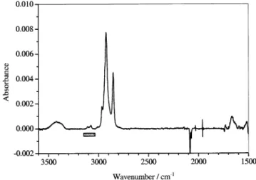
together with a broad absorption at 3420 cm-1attributed to
internally hydrogen bonded OsH (Figure 1). In the 3200-3000 cm-1region, several weak bands are visible, assigned to the
dCsH stretching of attached thiophene.22 The absorption at 1663 cm-1agrees well with that observed in the IR spectrum
of 1-(2-thienyl)-1-propanone23 at 1665 cm-1, indicating the
formation of 2-thienyl ketone units in the monolayer. Their presence can be reasonably explained by the steric constraints induced by the aromatic rings in the monolayer, which would inhibit disubstitution as the reaction nears completion.
Further evidence of the presence of the attached aromatic rings is provided by the HREELS analysis of the thiophene-terminated monolayer. As shown in Figure 2, the most intense bands are observed at 704, 836, 1064, 1235, 1430, and 3095 cm-1. The two first correspond to the dCsH out-of-plane
deformation and the CsSsC ring stretching, respectively.22,24,25
It must be noted that the presence of a band at 840-790 cm-1
is characteristic of 2-monosubstituted thiophenes26 and the
TABLE 1: Water Contact Angle, Thickness, and Infrared Absorptions of Ester- and Thiophene-Terminated
Monolayers surface θ(H2O)/dega φ/Åb positions of principal IR vibration bands/cm-1 1 72 16 2982, 2921, 2851, 1739 2 67 20 3420, 2923, 2851, 1663
aThe contact angles determined with water are thermodynamic
equilibrated values, which are believed to be smaller than advancing contact angles. Uncertainty (2°.bDetermined by ellipsometry.
Un-certainty (1 Å.
Figure 1. ATR-FTIR spectrum of 2. The negative peak at 2084 cm-1 is the Si-H stretch from the Si(111)-H surface that was used as the reference for background subtraction. The thiophene-stretching region is highlighted by the gray rectangle.
Figure 2. HREELS spectra of 2 at incident energies of 3 eV (solid line) and 6 eV (dashed line). Inelastic losses have not been normalized, and the elastic peak intensity is ∼3.4 times greater for the 3 eV spectrum.
absence of a signal in 1000-900 cm-1 region may serve as
indication that the ring is not substituted in the 3-position.27
The CsH in-plane bending vibrations are observed at 1064 and 1235 cm-1, whereas the bands at 1430 and 3095 cm-1 are
assignable to the CdC and CβsH stretching vibrations, respectively.
It is interesting to note that the methylene stretching vibration is also visible in the HREELS spectrum at ca. 2935 cm-1, but
its intensity is much smaller than that of bands characteristic of thiophene. This result contrasts with that obtained in IR and argues that the aromatic rings are covalently bound to the end of the alkyl chains, as the HREELS is more sensitive to functional groups at the surface of a film. Another interesting feature of the 3 eV HREELS spectrum is the observation of a weak feature at ∼2090 cm-1, attributed to the residual Si-H
stretch as it is known that the maximum coverage for alkyl modification of Si(111) is <0.5 ML.
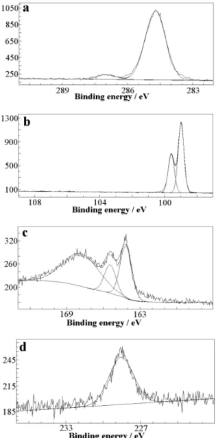
The nature of different chemical groups composing the organic films covalently bound to silicon and their atomic concentrations have been determined by XPS. The survey spectra taken at a takeoff angle of 45°are shown in Figure 3. They display characteristic peaks from the silicon substrate itself and from the C 1s and O 1s core levels of the attached organic molecule. For 2, two additional peaks corresponding to S 2s and S 2p are also observed. The absence of a F 1s signal in the spectrum of 1 which would appear at ∼686 eV binding energy, demonstrates that the ester-modified surface is not contaminated by Si-F species coming from the NH4F(aq)-etching reaction.
The high-resolution C 1s peak of 1 can be decomposed into three components at 285.0, 287.0, and 289.4 eV assigned to methylene, C-O, and C(O)O carbons, respectively. The peak areas are consistent with the ester structure. After reaction with the organolithium derivative, unresolved contributions from both thiophene (R, β) and polymethylene carbons give the main C 1s peak at 284.7 eV (Figure 4a) whereas the weak peak at 286.9 eV is reasonably attributed to the produced tertiary alcohol carbon. Indeed, the ratio of the peak areas is found to be ca. 16 which is close to the expected value for a ten-carbon chain terminated by a dithienyl carbinol moiety, i.e., 18. Moreover, the absence of a signal assignable to the ester carbon which would appear at higher binding energies corroborates the IR results and provides evidence for the complete conversion of reactive ester sites.
The Si 2p spectra of 1 and 2 can be deconvoluted into a doublet consisting of components from the 2p1/2 and 2p3/2Si
peaks located at 99.7-99.6 and 99.1-99.0 eV, respectively (Figure 4b).28,29The separations between these two peaks (0.6
eV) and their area ratios (∼0.55) are in close agreement with the theoretically expected values.28,29Furthermore, the formation
of silicon oxides resulting from the reaction of remained silicon hydrides with residual oxygen is not detected (i.e., absence of Figure 3. XPS survey spectra of freshly prepared (a) 1 and (b) 2.
Figure 4. XPS high-resolution spectra of (a) C 1s, (b) Si 2p, (c) S 2p, and (d) S 2s for 2.
a peak at binding energy 102-104 eV). However, it is important to note that the shift of the Si 2p peak is not a very sensitive measure of oxidation. Clearly, a large O 1s signal is observed for both 1 and 2 and analysis shows that oxygen is from 2- to 3-fold greater than the stoichiometric amount in both samples (Table 2). Because for 2, the atomic concentrations of carbon and sulfur determined from the peak areas are perfectly consistent with the monolayer composition involving the attachment of two thienyl rings at the end of each alkyl chain, the excess oxygen is probably not due to adventitious contami-nation of oxygen containing hydrocarbon species but rather oxidation of the Si interface.
As shown in Figure 3b, the survey spectrum of 2 reveals two sulfur signals corresponding to S 2p and S 2s. The S 2p high-resolution spectrum is composed of 2p3/2 and 2p1/2 peaks at
binding energies of 164.15 and 165.4 eV, respectively, which overlaps with one of the plasmon loss peak of the silicon substrate at 167.8 eV (Figure 4c).3cThe separation of S 2p1/2
and S 2p3/2 peaks (∼1.3 eV) and their area ratio (0.5) are in
agreement with the theoretical values determined from the spin-orbit splitting effect.30,31Moreover, the positions of these two
peaks are in accordance with earlier reported values for thiophene.24,32,33The S 2s signature appears at a binding energy
of 228.5 eV (Figure 4d) characteristic also of the aromatic ring.34,35Globally, the atomic ratios deduced from these XPS
results together with some IR observations (total loss of the initial ester stretch, weak intensity of the ketone band) indicate that the conversion of 1 into 2 is higher than 80% at least.
The absolute surface coverages of ester- and thiophene-terminated alkyl chains have been estimated from the procedure developed by Cicero et al.2ccombining XPS data with
ellipso-metric measurements. The photoelectron mean-free path pa-rameters for the monolayers and silicon substrate, which are involved in the analysis are the same as those used by Cicero et al. The considered film thicknesses are 16 and 20 Å for 1 and 2, respectively, as measured in this work. Accordingly, a value of 0.52 is found for the ester-terminated monolayer, which would indicate a maximum coverage of Si(111) as a theoretical limit of about 50% based on the diameter of an all-trans alkyl chain has been proposed by Linford et al.2bThis result suggests
the formation of reasonably dense layers, as already underlined from IR results. The coverage obtained for 2 is 0.42 dithienyl carbinol-terminated ten-carbon alkyl chain per surface silicon atom, which is also near the ideal structure. It must be pointed out that the uncertainty in these absolute coverage determinations is estimated as (30-50% because the attenuation lengths of photoelectrons used in the analysis have been measured for hydrocarbon films.36Therefore, the relatively small difference
in the coverage of 1 and 2 (ca. 0.1) is considered to be insignificant.
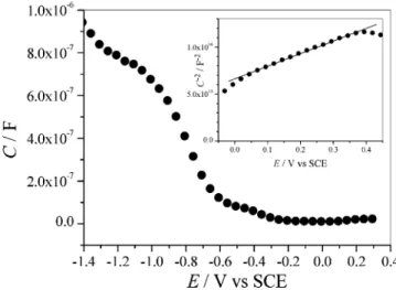
Electrochemical Characterization and Photoelectrochemi-cal Polymerization of Thiophene.The electrical properties of unmodified and modified Si(111) surfaces have been determined from differential capacitance and cyclic voltammetry measure-ments. Figure 5 shows the differential capacitance C vs potential Eresponse of 2 in contact with CH3CN + 10-1M Bu4NPF6.
The inset shows the Mott-Schottky plot (C-2vs E, eq 1) of
the above system, which is a measure of the space-charge layer under depletion conditions.37
where ǫ is the relative permittivity of silicon, ǫ0 is the
permittivity of free space, Nd is the dopant density of the
semiconductor, A is the area of the electrode, Efb is the
flat-band potential of the semiconductor electrode, k is the Boltz-mann constant, T is temperature, and q is the electronic charge. The shape and the position of both C-E and C-2-Eplots do
not depend on the nature of the counterion with ClO4-, giving
results similar to PF6-. A linear C-2-Eplot is obtained over ca. 0.5 V, the slope and the intercept of which enable the flat-band potential and the dopant density to be determined. The Nd
values obtained for Si(111)-H, 1 and 2 are nearly identical and are consistent with the dopant density derived from the four-probe resistivity measurements of these same silicon samples (Nd)(1.7 ( 0.3) × 1015cm-3). The values of Efbcalculated
for 1 and 2 are about the same (ca. -0.60 V) and in good agreement with other data reported for n-alkyl monolayers covalently bound to silicon (Table 3) in which the silicon is also significantly more depleted than the Si-H surface at open circuit.38These results are not surprising as the terminal groups
are probably too far from the semiconductor surface to influence band bending.
TABLE 2: Atomic Composition of 2 Derived from XPS High-Resolution Data
peak position/eV arearaw concn/%a normalizedconcn/%a,b concn/%c normalizedconcn/%b,c
O 1s 532.5 378.5 7.9 2.9 (1) 7.9 3.2 (1) C 1s 284.7 993.7 51.6 19.1 (19) 51.8 21.1 (19) 286.9 62.7 Si 2p 99.0 540.0 35.1 35.3 99.6 303.3 S 2p 164.15 164.5 5.4 2 (2) 165.4 87.6 167.8 311.9 S 2s 228.5 135.91 4.9 2 (2)
aCalculated from S 2p data (the third peak corresponding to the
silicon plasmon loss peak is not considered).bThe expected atomic
concentrations are in parentheses.cCalculated from S 2s data.
Figure 5. Differential capacitance (in dark, 1 kHz) of 2 in CH3CN + 10-1M Bu4NPF6as a function of the electrode potential. Inset shows the corresponding Mott-Schottky plot (C-2vs E) at 50 kHz.
TABLE 3: Differential Capacitance-Potential Properties of
Different Modified Si(111) Surfaces in CH3CN + 10-1M
Bu4NPF6, in the Dark
surface Nd/1015cm-3 a
open circuit
potential/V vs SCE Efb/V vs SCEa
Si(111)-H 1.6 ( 0.3 -0.27 ( 0.10 -0.46 ( 0.10
1 1.9 ( 0.4 0.08 ( 0.08 -0.56 ( 0.06
2 1.9 ( 0.4 0.13 ( 0.06 -0.61 ( 0.10
aThe dopant density Nd and the flat-band potential Efb were
calculated from the fitting of Mott-Schottky plots (C-2vs E; see text for details). All the data were averaged over 3-4 different unmodified and modified Si(111) surfaces.
C-2) 2
qǫǫ0NdA
2
(
E - Efb-kTq)
(1)This trend suggests the derivatization introduces surface states. The surface states responsible for the band bending are probably due to some oxidation of the Si(111) surface (unavoidable in the preparation of derivatized surfaces via photochemical reactions) and/or the possible presence of alkoxy species. Although there is no evidence for the formation of significant SiO2 from XPS analysis of these surfaces, the differential
capacitance measurements show a small plateau at ca. -0.5 V attributable to surface states in the gap (Figure 5). To evaluate the capacitance of the thiophene-terminated monolayer Cm, we
have used a model that has been successfully applied to alkyl modified silicon/electrolyte interfaces.38aIf the organic film is
considered as a capacitor between the semiconductor and the electrolyte, the total capacitance Ctot of 2 can be represented
where CSC is the space charge capacitance and CH is the
Helmholtz double-layer capacitance. A value of 1.1 µF cm-2
is determined for Ctot from the principal plateau at -1.1 V
(Figure 5). Using a CHvalue identical to that reported for other
analogous interfaces (3.5 µF cm-2) and neglecting the term
CSC-1in the case where E is negative to Efb,6c,38aCmis estimated
at 1.6 µF cm-2using eq 2. Now, the dielectric constant of the
thiophene-terminated monolayer, ǫm, can be determined from
eq 3 available for an ideal capacitor.
where φ is the thickness of the thiophene-terminated monolayer (20 Å). So, ǫmis found to equal 3.6. This value is in excellent
agreement with that of 3.3 ( 0.6 derived from the electrochemi-cal studies of n-alkyl monolayers on Si(111).38aIt suggests that
there are vacancies in the organic film through which solvent/ electrolyte may penetrate.
From the value of Efbexhibited by 2, it is obvious that the
anodic oxidation of attached di(2-thienyl)carbinol moieties can be observed only under illumination. Figure 6 shows the voltammetric behavior of 2 illuminated using an optical fiber (67 mW), in thoroughly dried CH3CN + 10-1M Bu4NPF6. An
irreversible anodic shoulder is observed at ca. 1.24 V vs SCE (0.02 V s-1). Comparison with 1 which is not redox active
within the same potential range suggests the electropolymer-ization of the pendant 2-thienyl units. If a second scan is recorded, this shoulder is no longer observed, indicating that most of the aromatic rings have reacted during the first scan.
As already demonstrated for 2-thienylcarbinols,39-41 it is
believed that the terminal moieties are converted into di(2-thienyl)methylcarbenium ions resulting from the elimination of the hydroxyl groups catalyzed by the protons liberated in the course of the electropolymerization process. Accordingly, the coupling of the 2-thienyl units would lead to a polymer, the conjugation of which is not interrupted. The surface coverage of the electroactive species Γ can be estimated from the current intensity of the anodic shoulder observed at 1.24 V using the voltammetric response of 1 as the background current (eq 4).42
where Ipais the anodic peak current intensity, R is the
charge-transfer coefficient assumed to be 0.5, n is the total number of electrons, na is the number of electrons involved in the
rate-determining step, F is the Faraday constant, and V is the potential scan rate. Assuming n ) na)2 electrons, a surface coverage
of 4.7 × 10⁻¹⁰ mol cm-2is obtained, which corresponds to
0.36 dithienyl carbinol-terminated ten-carbon alkyl chain per surface silicon atom considering the atomic density of Si(111) (7.8 × 10¹⁴atoms cm-2).6c This value is in good agreement
with the absolute surface coverage determined by XPS. To obtain higher coverage of a conducting material, the thiophene-terminated monolayer is photoelectrochemically oxi-dized in the presence of thiophene at 5 × 10⁻²M. Owing to
the possible photoanodic etching of underlying silicon in the presence of PF6-for potentials higher than 1.5 V vs SCE (Figure
6),43 the electropolymerization studies have been carried out
using a fluoride-free electrolytic anion, such as ClO4-. Under
these conditions, the cyclic voltammogram recorded for 2 reveals that the thiophene electropolymerization is catalyzed by the attached dithienyl carbinol moieties. As shown in Figure 7, the thiophene oxidation occurs with an onset at 1.14, 1.30, and 1.69 V on 2, Si(111)-H, and 1, respectively. Additionally, the crossing of forward and backward scans in the region of thiophene oxidation is a characteristic feature from the polym-erization-deposition of conducting polymers.44,45 For 2, the
catalytic phenomenon is believed to result from two contribu-tions. First, the steady state concentration of holes localized on the di(2-thienyl)carbinol moieties by irradiation will activate the thiophene electropolymerization. Indeed, it is expected that the generated holes efficiently tunnel through the n-alkyl chain to the immobilized redox centers.15Second, because the
di(2-thienyl)carbinol moieties exhibit an oxidation potential much lower than that of thiophene39a,46 (>400 mV), their presence
increases both the nucleation and deposition rates.
This is supported by both a larger charge under the cyclic voltammogram and slope of the current increase corresponding to the thiophene oxidation on 2 (Figure 7). Similar effects have been previously described for the electropolymerization of substituted thiophenes in the presence of bithiophene or ter-thiophene.47,48However, the electrocatalytic phenomenon
ob-served here is related to electropolymerizable groups immobi-lized on silicon and, to our knowledge, has never been reported before. After photoelectropolymerization the sequential p-doping and undoping of the electroformed polymer is illustrated by cyclic voltammetry. Polythiophene deposited on 2 exhibits a fully reversible and stable system at E°′)0.42 V (average of anodic and cathodic peak potentials) with a peak-to-peak separation ∆Epof 0-20 mV (Figure 7 bottom) as expected for
surface-confined redox species.49In contrast, the electrochemical
responses of the polymers deposited on 1 and Si(111)-H are largely shifted toward more positive potentials and much less reversible. Typically, E°′)0.68 and 0.73 V with ∆Ep)370 Figure 6. Cyclic voltammograms at 0.02 V s-1under illumination of
(a) 2 and (b) 1 in CH3CN + 10-1M Bu4NPF6.
Ctot -1) CSC -1+ Cm -1+ CH -1 (2) Cm-1)ǫφ mǫ0 (3) Ipa) (1-R)nnaF2AV 2.718RT Γ (4)
and 690 mV for polythiophene-coated Si(111)-H and 1, respectively. These differences are also evident for films photoelectrosynthesized at constant potential and tend to increase with increasing film thickness. The positive shift of the polymer system and the decrease of the electrochemical reversibility observed with Si(111)-H and 1 can be attributed to ohmic losses caused not only by a lack of the film adhesion on the electrode surface but also by a slower interfacial charge transfer between polythiophene and silicon that can be attributed to the absence of a covalent link. The polythiophene films grown on Si(111)-H are black and are easily removed from the electrode surface upon rinsing with an organic solvent, such as CH2Cl2
or THF. In contrast, polythiophene deposited on the thiophene-modified surface is green and is found to be remarkably adherent as it is not removed by sonication (e.g., 30 min in CH2Cl2) nor
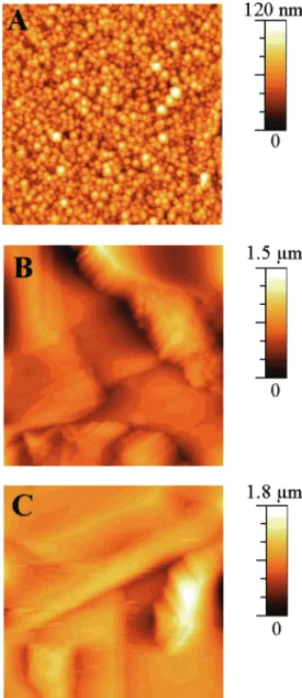
by the tape test. The case of 1 is intermediate because sonication of polymer-coated 1 reduces the film to a powder. Such a result can be related to the growth of the interpenetration of the conducting polymer segments into the alkyl chains of the organic monolayer likely due to enhanced nucleation at film defects. In addition to these adhesion differences, the polythiophene films deposited on unmodified and modified silicon surfaces are morphologically very different, as shown by AFM. Before photoelectropolymerization, contact-mode AFM images of 1 and 2reveal the atomically flat terraces of Si(111) with step heights of 0.32 ( 0.02 nm and a root-mean-square (rms) roughness of ca. 0.3 nm. Polymer deposited on 2 appears quite homogeneous
and smooth. The surface topography of this film is characterized by a globular structure with a roughness within the range 3-12 nm depending on the thickness (from 40 to ∼400 nm) (Figure 8A). In contrast, the films grown on Si(111)-H and 1 are heterogeneous and considerably rougher. By varying the thick-ness from 40 to ∼400 nm, their surfaces change from a globular to a very tortuous structure with the formation of large mountains and valleys (Figure 8B,C). For a 400 nm thick polymer, the measured roughness is 12-15 times higher than that determined for the polymer-modified 2.
The improvement in both adhesion and morphological properties has already been demonstrated for other poly-thiophene,50,51polyaniline,52or polypyrrole12a,53-58films
elec-trodeposited on monolayers incorporating the corresponding monomer. It highlights that the covalent attachment of the electropolymerizable units is required for improving the junction between the conducting material and the semiconductor.
Electrical Properties of Hybrid Polythiophene-Silicon Junctions Photoelectrogenerated from 2.To investigate the suitability of the polymer films photoelectrochemically grown on 2 for molecular device applications, ex situ measurements Figure 7. (Top) cyclic voltammograms corresponding to the anodic
electropolymerization under illumination (67 mW) of 5 × 10⁻² M thiophene onto (a) 2, (b) Si(111)-H, and (c) 1. (Bottom) electrochemi-cal responses of the corresponding ClO4--doped polythiophene films. Electrolytic solution: CH3CN + 10-1M Bu4NClO4. V ) 0.02 V s-1.
Figure 8. Contact-mode (10 × 10 µm2) AFM images for ca.
350-400 nm thick polythiophene films photoelectrodeposited at constant potential onto (A) 2, (B) Si(111)-H, and (C) 1. Measured rms roughnesses: 12 nm (A), ∼150 nm (B), and ∼170 nm (C).
of the electrical properties of these films were carried out. The polythiophene/decyl/Si(111) structures are expected to behave as metal-insulator-semiconductor (MIS) diodes, with charac-teristics similar to those of the metal/oxide/silicon structures used as gates in field effect transistors (MOSFETs).
Four probe measurements were used to measure the conduc-tivity of the films. Touching tungsten probes directly to the film yielded very high R > 10 MΩ contact resistances and often resulted in damage to the film. Therefore InGa drops were used to make lower resistivity, nondamaging contact to the film. The as grown films, doped with ClO4-, exhibit conductivities of ∼15
S cm-1, as measured in the collinear geometry. However, contact
resistances to these films were still rather high and variable, leading to large variations in the current-voltage characteristics of the polymer/silicon junctions. To improve the stability of their oxidized form, the as grown films were chemically reduced using triethylamine and subsequently doped with AuCl4-using
an acetonitrile solution containing gold trichloride.59 The
conductivity of these AuCl4-doped films was found to be more
uniform and could be measured by the van der Pauw method, yielding a sheet resistance of 2100 ( 50 Ω. As the film thickness was determined by AFM to be 200 nm, this corresponds to a conductivity of 24 S cm-1. It must be noted that a thinner film
(40 nm) exhibited a slightly lower conductivity of 8 S cm-1.
These films are observed to be photoconductive, as expected, with the sheet resistance decreasing to ∼500 Ω upon exposure to white light. The dark conductivity increases exponentially with temperature in the range 25-90°C and can be fit with an activation barrier of 66 meV. Some irreversible degradation of the conductivity at elevated temperatures is observed.
Although the four probe method extracts the film conductivity independent of the contact resistances, the current-voltage characteristics of the MIS structures are strongly influenced by the nature of the contact to the polythiophene. The initial characteristics of the InGa contacts indicated formation of a Schottky barrier (SB). A substantial SB is expected given the differences in work functions for InGa (4.2 eV) and poly-thiophene (5.1 eV) and the tendency of molecular semiconduc-tors to obey the Schottky-Mott rule (i.e., no Fermi level pinning).60However, the SB height is irreversibly reduced as
current is passed through the junction, resulting in the formation of ohmic contacts with a specific contact resistance of ∼10 Ω cm-2after currents >1 mA have been applied.
The capacitance versus voltage characteristics measured in the electrochemical cell have already been discussed above. Similar curves are obtained in the ex situ measurements (apart from the reverse sign conventions typical for electrochemical versus solid-state measurements). The Mott-Schottky plot (Figure 9) is of particular interest as the slope is proportional to 1/(NdA2), where Ndis the dopant density and A is the effective
area of the contact. Using the known value of the dopant density in our samples, the effective contact area is determined to be ∼0.3 cm2, in good agreement with the geometric area of the
polythiophene top contact. This indicates that the polythiophene is acting as a good metallic electrode (i.e., applying a negative voltage to a single point on the top contact results in depletion under the entire area of the contact). Efb is determined to be
1.2 eV, which is considerably higher than expected.
To determine relative alignments of the polythiophene and silicon Fermi levels (and perhaps shed light on the unexpectedly large Efb), we have also measured the surface potential of the
polythiophene/decyl/Si(111) junctions using a Kelvin probe. The Kelvin probe is a vibrating capacitor that measures the work function difference between the sample and a gold tip. As the work function of Au varies from 5.1 to 5.3 eV and is somewhat sensitive to ambient, absolute values of work function are
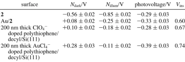
considerably less precise than our ability to measure work function differences so that differences in surface potential are reported in Table 4 below.
For 2, the surface potential in the dark is measured to be ∼4.65 eV (assuming the Au tip has a work function of 5.2 eV). For n-type silicon with an average dopant density of 2 × 10¹⁵
cm-3, the surface potential is expected to be at 4.35 eV. In fact,
surface potentials between 4.3 and 4.5 eV are measured on the Si(111)-H surface with the same bulk doping. The difference observed for 2 could be the result of either band bending or an interface dipole created by the chemical modification. These effects can be separated by measuring the surface potential under illumination where photogenerated electron-hole pairs act to screen the surface charge responsible for any band bending, thus flattening the bands. The difference between the surface potentials measured in the dark and under illumination is known as the photovoltage and is equal to the total amount of band bending (provided the light intensity is sufficient). From Table 4, it is apparent that there is substantial band bending at the thiophene terminated surface. This band bending is attributed to extrinsic oxidation of the interface during the modification reactions, as evidenced by the XPS data discussed above. It is important to note that even though the observed band bending is substantial, it only requires a surface charge density of 8.5 × 1010 cm-2. When Au is evaporated onto 2 to form a MIS
structure, the dark surface potential is similar to that of the Au tip, as expected. However, a substantial photovoltage is also observed that must result from light penetrating to the silicon interface. For a MIS structure with a thin insulating layer and in the absence of surface states, we would expect the contact potential difference (cpd) between the metal contact and the semiconductor to drop across the semiconductor. Instead, we find that for the Au/2 structure there is a substantial (0.6 V) drop across the organic insulating layer. This implies a significant (∼5 × 1012cm-2) density of surface states at the
silicon interface.
Figure 9. Mott-Schottky plot (100 kHz) for a 200 nm thick AuCl4 -doped polythiophene/decyl/Si(111) MIS structure produced from 2 and contacted by an InGa drop.
TABLE 4: Surface Potential Measurements for Several Different MIS Structures on Si(111) Produced from 2
surface Ndark/V Nillum/V photovoltage/V Vins 2 -0.56 ( 0.02 -0.85 ( 0.02 -0.29 ( 0.03 Au/2 +0.08 ( 0.02 -0.25 ( 0.02 -0.33 ( 0.03 0.60 200 nm thick ClO4 -doped polythiophene/ decyl/Si(111) +0.10 ( 0.02 -0.18 ( 0.02 -0.28 ( 0.03 0.67 200 nm thick AuCl4 -doped polythiophene/ decyl/Si(111) +0.28 ( 0.03 -0.11 ( 0.02 -0.39 ( 0.03 0.74
For the MIS structures employing polythiophene as the top contact, band bending at the surface of the polymer film and in the underlying Si could both contribute to the measured photovoltage (as the films are sufficiently thin to allow transmission of the light to the Si interface). However, due to the tendency of organic films to have low densities of gap states, we expect only small amounts of band bending at the polymer interface and so attribute the measured photovoltages to primarily arise from the underlying Si. The work function of the ClO4-doped polythiophene appears to be similar to that of
gold. The photovoltage of this structure is comparable to that for the Au top contact, again implying a substantial voltage drop across the insulating layer and a significant number of surface states at the interface. The increase in work function and concomitant increase in band bending upon doping the poly-thiophene with AuCl4-is consistent with the increased
con-ductivity of these films. Previous measurements on 3-substituted polythiophene films have highlighted that the work functions of the p-doped forms were strongly dependent on the substituent, the doping anion and the method of polymer synthesis.60,61The
surface state density, estimated from the voltage drop across the insulator, is only slightly increased by the doping procedure. These results suggest it may be possible to tune the properties of polythiophene/silicon junctions by adjusting the doping level in the polymer film, as evidenced by the increased band bending implying an increased SB height. Reducing the interface state densities will increase this tunability.
Having determined the energy level alignments in our MIS structures, we return to the question of the large Efb for the
AuCl4-doped polythiophene/Si(111) junctions determined from
the capacitance measurements. The measured flat band potential is 1.2 eV even though the band bending determined from the Kelvin probe measurements is ∼0.4 eV. These observations can be reconciled if there is a substantial density of surface states at the interface (7 × 1012cm-2) causing a large voltage drop
across the insulator.
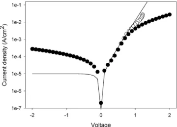
A typical current density (J)-voltage (V) characteristic of these AuCl4-doped polythiophene/decyl/Si(111) MIS structures
is shown in Figure 10.
The expected diode behavior due to SB formation at the alkyl/ Si(111) interface is clearly observed although the rectification is rather weak and the characteristics highly nonideal. The
deviation from diode behavior at forward biases >1 V is due to the effect of series resistance, due primarily to the contact resistance of the InGa/polythiophene contact.
The reverse characteristics do not saturate as expected but instead increase exponentially as V0.25. This functional form is
a signature of Schottky barrier lowering, the field-induced reduction of the SB height induced by the applied voltage.35
This effect is usually small for silicon diodes, and its prominence here suggests a rather low SB height <0.1 V. This low SB height is confirmed by the temperature dependence of the current-voltage characteristics, which indicates a similarly low value. The large discrepancy between the SB height determined from the current-voltage characteristics and that determined from the surface potential measurements (∼0.4 eV) suggests that these diodes are nonuniform with the lowest barrier paths dominating the transport.
This nonuniformity no doubt contributes to the large non-ideality factor of these diodes. Another factor contributing to the nonideality is the large surface state density in these devices already noted by the surface potential and capacitance measure-ments. These diodes can withstand large voltages with reverse breakdown not observed until V > 40 V. We note that many of the difficulties noted above appear to be related to the rather large area of these devices. Initial measurements on micron scale patterned devices suggest that these devices have much better rectification ratios (102-103) and ideality factors (∼2). This
work will be reported separately.62
IV. Conclusions
In this paper we have presented a detailed characterization of thiophene terminated Si(111) surfaces and photoelectro-chemical growth of polythiophene on these surfaces. The process outlined here leads to the formation of robust conducting polymer/silicon junctions in which the polymer is covalently linked to the silicon substrate through an alkyl spacer. The resulting doped polythiophene/decyl/Si(111) structures exhibit properties similar to other more conventional MIS diodes. These results suggest that this approach is promising for constructing hybrid molecular/silicon devices. The use of conducting polymer as a top contact for these devices should avoid problems due to metal penetration and/or damage to the organic layer associated with the evaporation of metal contacts. Furthermore, covalent bonding of the top contact to the device has potential advantages in terms of stability and lowering contact resistances.
For the simple devices studied here, surface states at the alkyl/ Si(111) interface were found to play a major role in determining the properties. Reducing these interface state densities is a major challenge for the fabrication of high quality molecular devices on silicon surfaces. Toward this goal, the organic functional-ization of Si(111) under thermal conditions and using a reagent, such as chlorotrimethysilane to trap the residual water, appears very promising to significantly lower the density of surface states.63
Acknowledgment. We are grateful to I. Sproule for invalu-able assistance with XPS measurements. S. A. Mitchell and M. Tomietto are also acknowledged for many helpful discussions and technical assistance. B. Fabre thanks NATO for a grant. References and Notes
(1) For reviews, see for example: (a) Buriak, J. M. Chem. ReV. 2002,
102, 1271-1308. (b) Wayner, D. D. M.; Wolkow, R. A. J. Chem. Soc.,
Perkin Trans. 2 2002, 23-34. (c) Bent, S. F. J. Phys. Chem. B 2002, 106, 2830-2842.
(2) (a) Linford, M. R.; Chidsey, C. E. D. J. Am. Chem. Soc. 1993,
115, 12631-12632. (b) Linford, M. R.; Fenter, P.; Eisenberger, P. M.; Chidsey, C. E. D. J. Am. Chem. Soc. 1995, 117, 3145-3155. (c) Cicero, R. L.; Linford, M. R.; Chidsey, C. E. D. Langmuir 2000, 16, 5688-5695.
Figure 10. Current density as a function of voltage for the 200 nm thick AuCl4-doped polythiophene/decyl/Si(111) MIS structure. The raw data are denoted by the filled circles whereas the hollow circles are the data corrected for series resistance (Rs)98 Ω). The solid line is a fit to the diode equation J ) J0[exp(qV/nkT) - 1],37 with the saturation current density J0)1 × 10⁻⁵A cm-2and the ideality factor
n )5.5.
(d) Wagner, P.; Nock, S.; Spudich, J. A.; Volkmuth, W. D.; Chu, S.; Cicero, R. L.; Wade, C. P.; Linford, M. R.; Chidsey, C. E. D. J. Struct. Biol. 1997,
119, 189-201. (e) Wade, C. P.; Chidsey, C. E. D. Appl. Phys. Lett. 1997,
71, 1679-1681.
(3) (a) Bansal, A.; Li, X.; Lauermann, I.; Lewis, N. S.; Yi, S. I.; Weinberg, W. H. J. Am. Chem. Soc. 1996, 118, 7225-7226. (b) Haber, J. A.; Lewis, N. S. J. Phys. Chem. B 2002, 106, 3639-3656. (c) Bansal, A.; Li, X.; Yi, S. I.; Weinberg, W. H.; Lewis, N. S. J. Phys. Chem. B 2001,
105, 10266-10277. (d) Bansal, A.; Lewis, N. S. J. Phys. Chem. B 1998, 102, 1067-1070.
(4) (a) Boukherroub, R.; Wayner, D. D. M. J. Am. Chem. Soc. 1999,
121, 11513-11515. (b) Boukherroub, R.; Morin, S.; Bensebaa, F.; Wayner,
D. D. M. Langmuir 1999, 15, 3831-3835. (c) Wojtyk, J. T. C.; Tomietto, M.; Boukherroub, R.; Wayner, D. D. M. J. Am. Chem. Soc. 2001, 123, 1535-1536. (d) Mitchell, S. A.; Ward, T. R.; Wayner, D. D. M.; Lopinski, G. P. J. Phys. Chem. B 2002, 106, 9873-9882. (e) Boukherroub, R.; Morin, S.; Sharpe, P.; Wayner, D. D. M.; Allongue, P. Langmuir 2000, 16, 7429-7434. (f) Boukherroub, R.; Morin, S.; Wayner, D. D. M.; Bensebaa, F.; Sproule, G. I.; Baribeau, J.-M.; Lockwood, D. J. Chem. Mater. 2001, 13, 2002-2011. (g) Wojtyk, J. T. C.; Morin, K. A.; Boukherroub, R.; Wayner, D. D. M. Langmuir 2002, 18, 6081-6087.
(5) (a) Sieval, A. B.; Demirel, A. L.; Nissink, J. W. M.; Linford, M. R.; van der Maas, J. H.; de Jeu, W. H.; Zuilhof, H.; Sudho¨lter, E. J. R.
Langmuir 1998, 14, 1759-1768. (b) Sieval, A. B.; Vleeming, V.; Zuilhof, H.; Sudho¨lter, E. J. R. Langmuir 1999, 15, 8288-8291. (c) Sieval, A. B.; Linke, R.; Heij, G.; Meijer, G.; Zuilhof, H.; Sudho¨lter, E. J. R. Langmuir
2001, 17, 7554-7559.
(6) (a) Henry de Villeneuve, C.; Pinson, J.; Bernard, M. C.; Allongue, P. J. Phys. Chem. B 1997, 101, 2415-2420. (b) Allongue, P.; Henry de Villeneuve, C.; Pinson, J.; Ozanam, F.; Chazalviel, J. N.; Wallart, X.
Electrochim. Acta 1998, 43, 2791-2798. (c) Allongue, P.; Henry de Villeneuve, C.; Pinson, J. Electrochim. Acta 2000, 45, 3241-3248.
(7) (a) Hart, B. R.; Le´tant, S. E.; Kane, S. R., Hadi, M. Z.; Shields, S. J.; Reynolds, J. G. Chem. Commun. 2003, 322-323. (b) Zhang, L.; Li, L.; Chen, S.; Jiang, S. Langmuir 2002, 18, 5448-5456. (c) Fellah, S.; Teyssot, A.; Ozanam, F.; Chazalviel, J.-N.; Vigneron, J.; Etcheberry, A. Langmuir
2002, 18, 5851-5860. (d) Lie, L. H.; Patole, S. N.; Hart, E. R.; Houlton,
A.; Horrocks, B. R. J. Phys. Chem. B 2002, 106, 113-120. (e) Roth, K. M.; Yasseri, A. A.; Liu, Z.; Dabke, R. B.; Malinovskii, V.; Schweikart, K.-H.; Yu, L.; Tiznado, H.; Zaera, F.; Lindsey, J. S.; Kuhr, W. G.; Bocian, D. F. J. Am. Chem. Soc. 2003, 125, 505-517.
(8) Ulman, A. Chem. ReV. 1996, 96, 1533-1554.
(9) Bain, C. D.; Troughton, E. B.; Tao, Y. T.; Evall, J.; Whitesides, G. M.; Nuzzo, R. G. J. Am. Chem. Soc. 1989, 111, 321-335.
(10) Walsh, R.; Becerra, R. In The Chemistry of Organic Silicon
Compounds; Rappaport, Z., Apeloig, Y., Eds.; Wiley-Interscience: Chi-chester, U.K., 1998; Vol. 2, pp 153-180.
(11) Dubois, L. H.; Nuzzo, R. G. Annu. ReV. Phys. Chem. 1992, 43, 437-463.
(12) (a) Kim, N. Y.; Laibinis, P. E. J. Am. Chem. Soc. 1999, 121, 7162-7163. (b) Vermeir, I. E.; Kim, N. Y.; Laibinis, P. E. Appl. Phys. Lett. 1999,
74, 3860-3862.
(13) Fabre, B.; Lopinski, G. P.; Wayner, D. D. M. Chem. Commun.
2002, 2904-2905.
(14) Royea, W. J.; Juang, A.; Lewis, N. S. Appl. Phys. Lett. 2000, 77, 1988-1990.
(15) (a) Selzer, Y.; Salomon, A.; Cahen, D. J. Am. Chem. Soc. 2002,
124, 2886-2887. (b) Cahen, D.; Hodes, G. AdV. Mater. 2002, 14,
789-798.
(16) (a) Paddon-Row: M. N.; Shephard, M. J.; Jordan, K. D. J. Phys.
Chem. 1993, 97, 1743-1745. (b) Shephard, M. J.; Paddon-Row: M. N. Chem. Phys. Lett. 1999, 301, 281-286.
(17) Hsu, C.; Marcus, R. A. J. Chem. Phys. 1997, 106, 584-598. (18) Sailor, M. J.; Klavetter, F. L.; Grubbs, R. H.; Lewis, N. S. Nature
1990, 346, 155-157.
(19) Chen, J.; Reed, M. A. Chem. Phys. 2002, 281, 127-145. (20) (a) Fischer, C. M.; Burghard, M.; Roth, S.; Klitzing, K. v. Appl.
Phys. Lett. 1995, 66, 3331-3333. (b) Burghard, M.; Philipp, G.; Mueller-Schwanneke, C.; Roth, S. Synth. Met. 1998, 94, 141-144.
(21) Snyder, R. G.; Strauss, H. L.; Elliger, C. A. J. Phys. Chem. 1982,
86, 5145-5150.
(22) Louarn, G.; Buisson, J. P.; Lefrant, S.; Fichou, D. J. Phys. Chem.
1995, 99, 11399-11404.
(23) Pouchert, C. J. The Aldrich Library of FT-IR spectra, 1st ed.; Aldrich Chemical Co., Inc.: 1985; Vol. 2, p 598-A.
(24) Liedberg, B.; Yang, Z.; Engquist, I.; Wirde, M.; Gelius, U.; Go¨tz, G.; Ba¨uerle, P.; Rummel, R.-M.; Ziegler, Ch.; Go¨pel, W. J. Phys. Chem. B
1997, 101, 5951-5962.
(25) Rei Vilar, M.; Horowitz, G.; Lang, P.; Pellegrino, O.; Botelho do Rego, A. M. AdV. Mater. Opt. Electron. 1999, 9, 211-218.
(26) Katritzky, A. R.; Boulton, A. J. J. Chem. Soc. 1959, 3500-3502. (27) Rosatzin, H. Spectrochim. Acta 1963, 19, 1107-1118.
(28) Tufts, B. J.; Kumar, A.; Bansal, A.; Lewis, N. S. J. Phys. Chem.
1992, 96, 4581-4592.
(29) Grunthaner, P. J.; Hecht, M. H.; Grunthaner, F. J.; Johnson, N. M.
J. Appl. Phys. 1987, 61, 629-638.
(30) Castner, D. G.; Hinds, K.; Grainger, D. W. Langmuir 1996, 12, 5083-5086.
(31) Ishida, T.; Hara, M.; Kojima, I.; Tsuneda, S.; Nishida, N.; Sasabe, H.; Knoll, W. Langmuir 1998, 14, 2092-2096.
(32) Tourillon, G.; Jugnet, Y. J. Chem. Phys. 1988, 89, 1905-1913. (33) Dannetun, P.; Boman, M.; Stafstro¨m, S.; Salaneck, W. R.; Laz-zaroni, R.; Fredriksson, C.; Bre´das, J. L.; Zamboni, R.; Taliani, C. J. Chem.
Phys. 1993, 99, 664-672.
(34) He, J.; Patitsas, S. N.; Preston, K. F.; Wolkow, R. A.; Wayner, D. D. M. Chem. Phys. Lett. 1998, 286, 508-514.
(35) Qiao, M. H.; Cao, Y.; Tao, F.; Liu, Q.; Deng, J. F.; Xu, G. Q. J.
Phys. Chem. B 2000, 104, 11211-11219.
(36) Bain, C. D.; Whitesides, G. M. J. Phys. Chem. 1989, 93, 1670-1673.
(37) Sze, S. M. The Physics of Semiconductor DeVices, 2nd ed.; Wiley: New York, 1981.
(38) (a) Yu, H.-Z.; Morin, S.; Wayner, D. D. M.; Allongue, P.; Henry de Villeneuve, C. J. Phys. Chem. B 2000, 104, 11157-11161. (b) Yu, H.-Z.; Boukherroub, R.; Morin, S.; Wayner, D. D. M. Electrochem. Commun.
2000, 2, 562-566.
(39) (a) Marrec, P.; Simonet, J. J. Electroanal. Chem. 1998, 459, 35-44. (b) Fabre, B.; Marrec, P.; Beaugy, C.; Simonet, J. J. Electroanal. Chem.
1998, 455, 5-9.
(40) Hoffmann, K. J.; Graskopf, A. L.; Samuelsen, E. J.; Carlsen, P. H. J. Synth. Met. 2000, 113, 89-92.
(41) Abarca, B.; Asensio, G.; Ballesteros, R.; Varea, T. J. Org. Chem.
1991, 56, 3224-3229.
(42) Bard, A. J.; Faulkner, L. R. Electrochemical Methods. Fundamentals
and Applications; Wiley: New York, 1980; p 525.
(43) Fabre, B.; Wayner, D. D. M. Manuscript in preparation. (44) Asavapiriyanont, S.; Chandler, G. K.; Gunawardena, G. A.; Pletcher, D. J. Electroanal. Chem. 1984, 177, 229-244.
(45) Zotti, G.; Cattarin, S.; Comisso, N. J. Electroanal. Chem. 1987,
235, 259-273.
(46) Waltman, R. J.; Bargon, J.; Diaz, A. F. J. Phys. Chem. 1983, 87, 1459-1463.
(47) Zhao, Z. S.; Pickup, P. G. J. Electroanal. Chem. 1996, 404, 55-60.
(48) (a) Wei, Y.; Chan, C.-C.; Tian, J.; Jang, G.-W.; Hsueh, K. F. Chem.
Mater. 1991, 3, 888-897. (b) Wei, Y.; Tian, J. Macromolecules 1993, 26,
457-463.
(49) Bard, A. J.; Faulkner, L. R. Electrochemical Methods. Fundamentals
and Applications; Wiley: New York, 1980; p 522.
(50) Kang, J. F.; Perry, J. D.; Tian, P.; Kilbey, S. M. Langmuir 2002,
18, 10196-10201.
(51) Inaoka, S.; Collard, D. M. Langmuir 1999, 15, 3752-3758. (52) Li, Z. F.; Ruckenstein, E. Macromolecules 2002, 35, 9506-9512. (53) Willicut, R. J.; McCarley, R. L. Langmuir 1995, 11, 296-301. (54) Rubinstein, I.; Rishpon, J.; Sabatani, E.; Redondo, A.; Gottesfeld, S. J. Am. Chem. Soc. 1990, 112, 6135-6136.
(55) Simon, R. A.; Ricco, A. J.; Wrighton, M. S. J. Am. Chem. Soc.
1982, 104, 2031-2034.
(56) Sayre, C. N.; Collard, D. M. Langmuir 1995, 11, 302-306. (57) Wurm, D. B.; Brittain, S. T.; Kim, Y.-T. Langmuir 1996, 12, 3756-3758.
(58) Wu, C.-G.; Chiang, S.-C.; Wu, C.-H. Langmuir 2002, 18, 7473-7481.
(59) (a) Abdou, M. S. A.; Holdcroft, S. Chem. Mater. 1996, 8, 26-31. (b) Abdou, M. S. A.; Holdcroft, S. Synth. Met. 1993, 60, 93-96.
(60) Kinbara, E.; Kunugi, Y.; Harima, Y.; Yamashita, K. Synth. Met.
2000, 114, 295-303.
(61) Chowdhury, A.-N., Kunugi, Y.; Harima, Y.; Yamashita, K. Thin
Solid Films 1995, 271, 1-3.
(62) Lopinski, G. P.; Fabre, B.; Wayner, D. D. M. Manuscript in preparation.
(63) Boukherroub, R.; Wayner, D. D. M.; Sproule, G. I.; Lockwood, D. J.; Canham, L. T. Nano Lett. 2001, 1, 713-717.