Publisher’s version / Version de l'éditeur:
International Journal of High Speed Electronics and Systems, 26, 1 & 2, 2017-03
READ THESE TERMS AND CONDITIONS CAREFULLY BEFORE USING THIS WEBSITE. https://nrc-publications.canada.ca/eng/copyright
Vous avez des questions? Nous pouvons vous aider. Pour communiquer directement avec un auteur, consultez la première page de la revue dans laquelle son article a été publié afin de trouver ses coordonnées. Si vous n’arrivez Questions? Contact the NRC Publications Archive team at
[email protected]. If you wish to email the authors directly, please see the first page of the publication for their contact information.
NRC Publications Archive
Archives des publications du CNRC
This publication could be one of several versions: author’s original, accepted manuscript or the publisher’s version. / La version de cette publication peut être l’une des suivantes : la version prépublication de l’auteur, la version acceptée du manuscrit ou la version de l’éditeur.
For the publisher’s version, please access the DOI link below./ Pour consulter la version de l’éditeur, utilisez le lien DOI ci-dessous.
https://doi.org/10.1142/S0129156417400055
Access and use of this website and the material on it are subject to the Terms and Conditions set forth at
Integrated on-chip nano-optomechanical systems
Diao, Zhu; Sauer, Vincent T. K.; Hiebert, Wayne K.
https://publications-cnrc.canada.ca/fra/droits
L’accès à ce site Web et l’utilisation de son contenu sont assujettis aux conditions présentées dans le site LISEZ CES CONDITIONS ATTENTIVEMENT AVANT D’UTILISER CE SITE WEB.
NRC Publications Record / Notice d'Archives des publications de CNRC:
https://nrc-publications.canada.ca/eng/view/object/?id=f623a5e8-be16-4b72-8372-fb220a7febce https://publications-cnrc.canada.ca/fra/voir/objet/?id=f623a5e8-be16-4b72-8372-fb220a7febceVol. 26, Nos. 1 & 2 (2017) 1740005 (22 pages) c
World Scientific Publishing Company DOI: 10.1142/S0129156417400055
Integrated On-Chip Nano-Optomechanical Systems
Zhu Diao∗
Department of Mathematics, Physics and Electrical Engineering, Halmstad University, Box 823, SE-301 18 Halmstad, Sweden
[email protected] Vincent T. K. Sauer
National Institute for Nanotechnology, 11421 Saskatchewan Drive, Edmonton T6G 2M9, Alberta, Canada
Department of Electrical and Computer Engineering, University of Alberta, 9211-116 Street NW, Edmonton T6G 1H9, Alberta, Canada
and
Department of Biological Sciences, CW 405, Biological Sciences Bldg., University of Alberta, Edmonton T6G 2E9, Alberta, Canada
[email protected] Wayne K. Hiebert
National Institute for Nanotechnology, 11421 Saskatchewan Drive, Edmonton T6G 2M9, Alberta, Canada
and
Department of Physics, University of Alberta, 4-181 CCIS, Edmonton T6G 2E1, Alberta, Canada
Received 30 September 2016 Accepted 30 November 2016
Recent developments in integrated on-chip nano-optomechanical systems are reviewed. Silicon-based nano-optomechanical devices are fabricated by a two-step process, where the first step is a foundry-enabled photonic circuits patterning and the second step involves in-house mechanical device release. We show theoretically that the enhanced responsivity of near-field optical transduction of mechanical displacement in on-chip nano-optomechanical systems originates from the finesse of the optical cavity to which the mechanical device couples. An enhancement in responsivity of more than two or-ders of magnitude has been observed when compared side-by-side with free-space in-terferometry readout. We further demonstrate two approaches to facilitate large-scale device integration, namely, wavelength-division multiplexing and frequency-division
∗Previous address: National Institute for Nanotechnology, 11421 Saskatchewan Drive, Edmon-ton T6G 2M9, Alberta, Canada and Department of Physics, University of Alberta, 4-181 CCIS, Edmonton T6G 2E1, Alberta, Canada.
Int. J. Hi. Spe. Ele. Syst. 2017.26. Downloaded from www.worldscientific.com
multiplexing. They are capable of significantly simplifying the design complexity for addressing individual nano-optomechanical devices embedded in a large array. Keywords: Nanomechanical resonators; Nano-optomechanical systems; Nanophotonics.
1. Introduction
Rapid developments in nanotechnology and nanoelectronics have made it possi-ble to routinely design and fabricate devices and systems with functional blocks in the sub-micrometer scale. The current wave of ”More than Moore” technology, which focuses on device functionalities rather than merely packing up more and more transistors into a smaller and smaller chip area, has led to the emergence of a wide range of innovative devices with their potential applications in remote sens-ing, point-of-care testsens-ing, and high-bandwidth signal processing.1
Among them, microfabricated highfrequency nanomechanical resonators operated in the MHz -GHz frequency range have attracted a growing amount of attention.2,3 These de-vices take full advantage of the flexibility and robustness offered by precisely-tuned nanometer-scale mechanical structures, and have been utilized as ultra-sensitive surface force gauges,4,5 inertial mass sensors,6,7,8,9 magnetometers,10,11,12,13,14
thermometers,15,16 memory cells,17 accelerometers,18and clocking references.19
One of the factors which so far have limited further developments and wide adoption of nanomechanical resonators is how the diminutive displacement involved while operating these resonators (typically in the sub-nanometer scale) may be effec-tively transduced with a GHz-plus bandwidth. In nanoelectromechanical systems (NEMS), the mechanical displacement is actuated as well as sensed electrically, i.e.through a selection of capacitive,20,21,22piezoelectric,23,24 piezoresistive,25,26,27
electron tunnelling,28,29 and electrothermal30 methods or a combination of several
of them together. These tranduction schemes often rely on on-chip integrated signal amplifiers, e.g. single-electron transistors (SET)31,32or high-electron-mobility
tran-sistors (HEMT)33,34 to enhance the relatively small electrical signal induced by
de-vice displacement, and complicated down-mixing circuits to bypass the bandwidth limitation.22,26,27,29,30 Such approaches drastically increase the design complexity
and very often limit the operating temperatures and applicable areas of NEMS. Free-space optical methods have long been utilized to transduce the motion of nanomechanical resonators.35,36,37,38,39 Compared with electrical transduction,
high-bandwidth operation is easily achieved without signal down-mixing. However, due to natural constrains of the optical wavelength, upon scaling down, physical dimensions of nanomechanical resonators quickly reach the diffraction limit of the laser wavelength in use.40 Most of the input laser beam then undergoes a
diffrac-tion process rather than reflecdiffrac-tion, strongly reducing the intensity of light that can be captured on the photodetector. Hence, the signal-to-noise ratio of the readout quickly diminishes. Furthermore, stringent requirements on the relative alignment of the laser spot and the nanomechanical device hinders large-scale device inte-gration. Nano-optomechanical systems (NOMS), where on-chip integrated optical
Int. J. Hi. Spe. Ele. Syst. 2017.26. Downloaded from www.worldscientific.com
circuits are utilized to transduce the motion of nanomechanical resonators in the optical near-field, form a significant development in the last decade.41,42,43,44,45 It
overcomes the diffraction limit by moving the interaction from far-field to near-field, while maintaining the high bandwidth offered by an optical transduction scheme. Taking advantage of high-finesse on-chip optical cavities, where individ-ual photons can interact multiple times with a nanomechanical device before they are dissipated, the responsivity of NOMS displacement transduction has reached an unprecedented level in recent years.46,47,48,49 It was further demonstrated that
the optical gradient force existing in the near-field of a guided light wave can be harnessed to excite the nanomechanical device, making possible full-optical pump-probe operation.50,51,52,53Moreover, developments in NOMS coincide with the rapid advancement of silicon-based nanophotonics technology,54
providing a clear path-way for chip-level device integration.
Driving forces behind the rapid expansion of NOMS research in the last decade have been and are still of two folds. One is the pursuing of a deep understanding of the quantum nature of our universe, in which researchers are trying to create macro-scopic quantum mechanical systems by realizing strong coupling between mechani-cal resonators and cavity fields (the so-mechani-called cavity optomechanics).55,56,57,58,59,60
The other is the demand of the microelectronics and nanophotonics industry to develop mechanically-active functional devices in the nanometer scale and estab-lish highly-sensitive, reliable, low-cost, highly-integrable transduction schemes to monitor their displacement.41,43,45,51,52,61 Hence, NOMS is a perfect modern-day
example where cutting-edge fundamental science meets innovative industry devel-opment. While we emphasize that the two aspects are both of paramount impor-tance in the advancement of NOMS technology, in our current report, we will limit ourselves mostly to the later aspect.
Here we review recent developments in high-frequency integrated NOMS real-ized on the silicon-on-insulator platform. These devices are compatible with state-of-the-art silicon photonics technology, thus, hold the promise to be implemented imminently in a large variety of applications as sensors, actuators, and frequency references. In Section 2, we outline the theoretical background of NOMS transduc-tion in the linear regime and in Sectransduc-tion 3, the device fabricatransduc-tion process is explained. Our discussion here pays particular attention to the fact that integrated NOMS can be mass manufactured in a similar process as that used to fabricate silicon photonic circuits. Hence, it is especially suitable for large-scale device integration. Measure-ment results on a selective subset of our NOMS devices are presented in Section 4, with a focus on how NOMS technology may move from its current state of address-ing individual devices to chip-level multiplexaddress-ing and multi-scale integration, before conclusions are made in Section 5.
Int. J. Hi. Spe. Ele. Syst. 2017.26. Downloaded from www.worldscientific.com
2. Theory of Device Displacement Transduction
A comprehensive theoretical description of the problem in which a nanome-chanical resonator couples to an optical cavity requires the language of cavity optomechanics.57,59,60 It not only takes account of the effective refractive index
change of the cavity as a result of the displacement of the mechanical object, but also a ‘back-action’ exerted by the cavity to it. However, when the finesse of the optical cavity is low, the opto-mechanical coupling is relatively weak, and the me-chanical displacement in concern is small, the discussion may be simplified to the linear regime, where the effect of the ‘back-action’ can be neglected. This is the approach we adopt. We will show later in this section that such assumptions hold in our NOMS devices and this simplified theoretical treatment is supported by our experimental data.
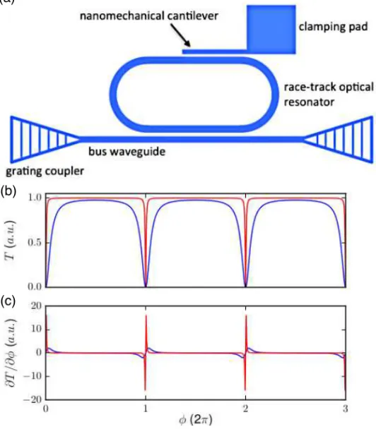
From now on, we will focus our discussion on one of the simplest cases in which an optical ring or race-track cavity is coupled to a bus waveguide in the all-pass filter configuration on one side and a released cantilever or a doubly-clamped mechanical beam is coupled to the same cavity on the opposite side. A sketch of such a device is shown in Fig. 1(a). Light is coupled into the photonic circuit through grating couplers.62
The bus waveguide carries light to the race-track optical cavity and also carries light away from it to the output grating coupler. The transmission coefficient of such a device goes through a series of dips when the wavelength of the incoming light satisfies the cavity resonance condition as shown in Fig. 1(b). More specifically, the transmission coefficient can be expressed as63,64,65
T = T0+ [(2/π)F · sin(φ/2)]
2
1 + [(2/π)F · sin(φ/2)]2 . (1)
where T0 is the on-resonance residual transmission determined by the coupling
between the cavity and the waveguide, φ = (2πλ)neffL is the round-trip phase
accu-mulation, in which λ denotes the vacuum wavelength, neff is the effective refractive
index and L is the round-trip distance, and F = FSR/(2δλ) is the finesse of the optical cavity. The (wavelength) free-spectral range, FSR, is the separation in wave-length of adjacent minima in the transmission coefficient and 2δλ is the full-width-at-half-maximum of a specific resonance mode.66
A parameter closely-related to the FSR is the optical cavity quality factor, Qo = (neffL/λ)F. Finesse is governed by
the round-trip cavity loss and does not directly depend on the length of the cavity, whereas Qo is a function of both parameters. We will see later that the efficiency
of displacement transduction in NOMS depends solely on the finesse of the cavity, hence, the transduction responsivity cannot be enhanced by merely increasing the length of the cavity to obtain apparently ‘sharp’ cavity resonances while plotted as a function of wavelength.
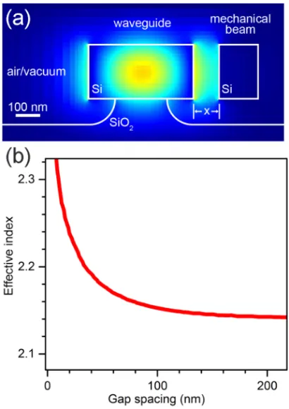
Displacement of the mechanical resonator (denoted as x) tunes the effective refractive index of the section of the optical cavity coupled to it, as shown in Fig. 2. When the mechanical resonator moves closer to the race-track optical cavity, the effective refractive index increases. The slope expressed as ∂neff/∂x can be
Int. J. Hi. Spe. Ele. Syst. 2017.26. Downloaded from www.worldscientific.com
extremely large as seen in Fig. 2(b) when the gap between the mechanical resonator and the cavity is small. The refractive index change in turn modifies the round-trip phase accumulation, the position of the cavity mode and the transmission coefficient of the system. One can write64,65
∂T ∂x = ∂T ∂φ ∂φ ∂x. (2)
It is important to note that the first term on the right hand side of Eq. (2) is an intrinsic property of the all-pass optical filter consisted of the optical cavity and the input bus waveguide while the second term describes the strength of coupling between the mechanical resonator and the cavity. To achieve high transduction responsivity, one has to optimize ∂T /∂x.
���
���
���
Fig. 1. (a) A sketch showing a nanomechanical cantilever coupling to an on-chip all-pass filter. The components are not drawn to scale. (b) The transmission coefficient of an all-pass filter with F = 10 (blue) and F = 100 (red). (c) The derivative of the transmission coefficient, ∂T /∂φ, for F= 10 (blue) and F = 100. T0 in Eq.(1) is set to zero in (b) and (c).
Int. J. Hi. Spe. Ele. Syst. 2017.26. Downloaded from www.worldscientific.com
Fig. 2. (a) The simulated optical mode in a partially underetched waveguide adjacent to a released mechanical beam. The waveguide is 430 nm wide and the width of the mechanical beam is 160 nm. The distance between them is 100 nm. The waveguide forms part of a race-track optical cavity. (b) The waveguide effective refractive index as a function of its distance to the mechanical resonator.
Maxima in |∂T/∂φ| occur when ∂2
T /∂φ2 goes to zero.64,65 ∂T ∂φ max ≈ 3 √ 3 8π (1 − T0)F. (3) and sin(φ 2) |∂T ∂φ| at max ≈ ± π 2√3F. (4)
Experimentally, using a tunable diode laser, one often sets the probe laser wave-length to where the transmission coefficient as a function of laser wavewave-length has the maximum slope, |∂T/∂λ|max. Strictly speaking, this is not the same condition
as defined in Eqs. (3) and (4), since ∂φ ∂λ = − 2πneffL λ2 + ( 2πL λ )( ∂neff ∂λ ). (5)
Int. J. Hi. Spe. Ele. Syst. 2017.26. Downloaded from www.worldscientific.com
Only when the chromatic dispersion of the waveguide, ∂neff/∂λ, can be ignored,
may the two conditions converge. The second term on the right hand side in Eq. (2) can be further expanded as65
∂φ ∂x = ( 2π λ ) · ( ∂neff ∂x ) · β · l. (6)
in which l is the length of the nanomechanical device and β takes account into the mode shape of the mechanical resonance.67
Inserting Eqs. (3) and (6) into Eq. (2), one obtains the maximum transduction responsivity of a NOMS device
∂T ∂x max = 3 √ 3 8π · (1 − T0) · F · ( 2π λ) · ( ∂neff ∂x ) · β · l. (7)
We approximate the frequency response of the mechanical resonator as a high-Q harmonic oscillator, which can be described by a Lorentzian function.
Sx(f ) = [F0(f )/4π2meff]2 (f2− f2 0)2+ ( f f0 Qm) 2. (8)
in which Sx(f ) is the power spectral of the mechanical displacement, F0(f ) is the
magnitude of the frequency-dependent driving force, meff is the effective mass of the
resonator, and f0 is the mechanical resonance frequency. At a finite temperature
with no apparent external driving force, the thermal bath provides a wide-band excitation to a mechanical device and its response is governed by Eq. (8), the so-called thermomechanical (TM) noise. Since the system has only a single degree of freedom, its TM noise can be calibrated utilizing the equipartition theorem
1 2kBT = 1 2khx 2 i. (9)
where kB is the Boltzmann constant, and k = (2πf0)2meff is the effective spring
constant of the mechanical resonator. This provides a unique way to confirm the validity of Eq. (7), since the TM displacement is known from Eq. (9), ∂T /∂λ and F can be obtained from the device DC transmission spectrum, β and l are both geometrical parameters, and ∂neff/∂x can be worked out through simulations. Such
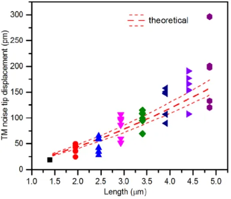
validity tests have been carried out with a series of nanomechanical cantilevers of different lengths and placed at different distances away from the race-track optical cavity in Ref. 65, and the results are shown in Fig. 3. For this series of devices, the finesse of the race-track optical resonators is between 50 and 70, whereas the nanomechanical cantilevers are placed 90 - 160 nm away from the optical cavities. The close correspondence between the theory and the experiment demonstrates that our theoretical framework is sufficient to describe the responsivity of NOMS devices in the low-finesse, low-optomechanical-coupling limit where the cavity ‘back-action’ is weak.
Int. J. Hi. Spe. Ele. Syst. 2017.26. Downloaded from www.worldscientific.com
Fig. 3. The cantilever tip displacement caused by thermomechanical noise. The different data points for each length come from devices with varying measured gap spacing. The spread in the data for each length is due to the slight variation in resonator widths with different gap sizes due to proximity effects during fabrication. Smaller gaps pair with slightly thicker and stiffer beams. The red dashed lines are the calculated theoretical values for the average beam thickness of 160 ± 10 nm. Reprinted from V. T. K. Sauer, Z. Diao, M. R. Freeman, and W. K. Hiebert, “Optical racetrack resonator transduction of nanomechanical cantilevers”, Nanotechnology 25 (2014) 055202 with permission from IOP publishing.
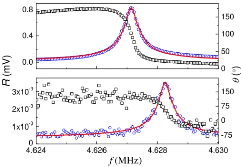
From Eq. (7), we see that the enhancement in transduction responsivity in NOMS readout, when compared with conventional free-space interferometry, orig-inates largely from the finesse of the on-chip optical cavity. In our samples, the finesse of the optical cavity falls in the range of 20 - 150 while the Fabry-P´erot cav-ity formed by the top and bottom silicon layers as end ‘mirrors’ in SOI-based devices usually has a finesse in the order of 1. Thus, an improvement in the responsitivity of the same order of magnitude may be expected. In Fig. 4, we show a side-by-side comparison of NOMS transduction and free-space interferometry transduction of the same nanomechanical doubly clamped beam, under the same excitation ampli-tude provided by a piezo disk.68
The mechanical resonance mode is at ∼ 4.628 MHz and the quality factor Qm ∼ 12,000. NOMS transduction leads to a slightly lower
resonance frequency which can be attributed to the optical spring effect.69The
on-chip race-track cavity utilized to transduce the mechanical motion in the NOMS design has a finesse F ∼ 134 and the corresponding responsivity improvement is ∼ 150× (the peak response is 0.8 mV for NOMS readout with a laser power of 47 µW and only 3 µV for free-space readout with a laser power of 28 µW), closely following the above discussion.
Int. J. Hi. Spe. Ele. Syst. 2017.26. Downloaded from www.worldscientific.com
4.6240 4.626 4.628 4.630 1x10⁻³ 2x10⁻³ 3x10⁻³ -75 0 75 150 0 50 100 150 R ( m V ) f (MHz) ( ° ) 0.0 0.4 0.8
Fig. 4. Driven mechanical response of an l = 15 µm doubly clamped beam embedded in a race-track resonator measured by nanophotonic (top panel) and free-space interferometry readout (bottom panel). The optical power in/on the device is 47 µW for the NOMS readout whereas 28 µW for the free-space interferometry readout. Blue circles represent the amplitude signal while black squares represent the phase signal. Red lines are Lorentzian fits to the data. Adapted from Z. Diao, J. E. Losby, V. T. K. Sauer, J. N. Westwood, M. R. Freeman, and W. K. Hiebert,“Confocal scanner for highly sensitive photonic transduction of nanomechanical resonators”, Appl. Phys. Express 6 (2013) 065202 with permission from the Japan Society of Applied Physics.
3. Device Fabrication
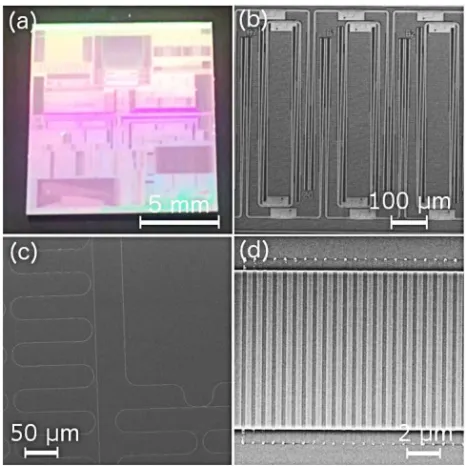
One of the major advantages of NOMS is that they can be fabricated in a simi-lar process as that commonly used to produce state-of-the-art silicon-on-insulator (SOI) photonics, indicating a clear pathway for wafer-scale manufacturing. It also allows NOMS to leverage the vast readily available infrastructure in silicon technol-ogy and be fused seamlessly into conventional integrated circuit chips. We take full advantage of this fact by outsourcing the bulk of device fabrication work to silicon photonics foundries. More specifically, nanophotonic circuits presented in this work were fabricated by either LETI in Grenoble, France or IMEC in Leuven, Belgium through their multi-project wafer services. Their standard processes are both built upon 200 mm SOI wafers with 220 nm silicon device layers on top of 2 µm buried oxides (BOX). Wafers are exposed by either 248 nm or 193 nm deep UV lithog-raphy with a minimum achievable feature size of ∼ 120 nm. Centimeter-sized dies housing thousands of silicon photonic circuit designs are fabricated in a single run. Figure 5(a) is an optical image of a silicon photonic chip fabricated by IMEC while Fig. 5(b) – (d) show a number of zoom-in SEM images recorded upon various silicon nanophotonic components.
NOMS devices are then formed in a second in-house processing step during which predefined sections of the top silicon device layer are mobilized from the BOX using SiOxwet etching, forming nanomechanical resonators. Resist layers patterned
Int. J. Hi. Spe. Ele. Syst. 2017.26. Downloaded from www.worldscientific.com
Fig. 5. (a) Full-view optical image of a silicon photonic chip containing a large number of NOMS devices fabricated by IMEC, Leuven, Belgium. (b) SEM image of a set of twelve adjacent photonic circuits on the same chip. (c) Zoomed-in view of photonic waveguides. (d) Zoomed-in view of a grating coupler used to couple light in and out of the photonic chip.
by either UV lithography or electron beam lithography are used to protect the rest of the chip surface during the oxide etch. Alternatively, a timed wet etching process has also been developed to release nanomechanical devices with widths less than that of silicon photonic waveguides.45
In Fig. 6, we present high-magnification SEM images of a number of completed NOMS devices. Resonance frequencies of our NOMS devices are designed to be in the range of several megahertz to several tens of megahertz, thus, in the high frequency (HF) band of the radio spectrum.
We note that our device fabrication process is of good reproducibility. Relatively little variation in device mechanical as well as optical properties can be identified in devices fabricated in the same processing run. In Fig. 7, we summarize the mechan-ical resonance frequency, f0, and the mechanical quality factor, Qm, of a number of
NOMS doubly clamped beams with nominally the same physical dimensions. One can easily see that variations in both f0 and Qm between device and device are
fairly small, with the standard deviation in f0being less than 2% of hf0i. Although
the standard deviation in Qmis larger, it still only amounts to 18% of hQmi.
Fur-ther improvement in the conformity of the device mechanical quality factor may be gained through fine control of clamping losses in the device design.70,71
Int. J. Hi. Spe. Ele. Syst. 2017.26. Downloaded from www.worldscientific.com
Fig. 6. SEM images of released NOMS devices. (a) A cantilever coupled to an on-chip Mach-Zehnder interferometer. (b) The same device as in (a) under high magnification. Electron beam charging causes the cantilever to vibrate during imaging. (c) A doubly clamped beam coupled to a race-track optical cavity. (d) A doubly clamped beam coupled to the partially etched BOX layer. (e) Double NOMS beams. (f) A doubly clamped beam with clamping pads.
4. Measurement Results
NOMS devices are housed in a vacuum chamber which can be pumped down to < 1×10⁻⁵Torr to eliminate air damping. The custom designed measurement setup
was previously described in Ref. 68, where one and the same microscope objective is utilized to both couple light into the photonic chip and retrieve light coming out of it. A two-wavelength, pump-probe transduction scheme is adopted in which a pump laser wavelength-tuned to an optical cavity mode is used to drive the mechanical displacement of the NOMS device through the optical gradient force while a separate probe laser with its wavelength tuned to the maximum sensitivity point (as described in Section 2) is utilized to probe the mechanical motion.50,51,52
Alternatively, a piezodisk attached to the backside of the sample can also be used
Int. J. Hi. Spe. Ele. Syst. 2017.26. Downloaded from www.worldscientific.com
(b)
(a)
(a)
13.6 14.0 14.4 6.0x10³ 9.0x10³ 1.2x10⁴ 1.5x10⁴Q
mf
0(MHz)
(a)
Fig. 7. (a) False-colored SEM image of a NOMS device tested. The device operates by near-field coupled to the partially etched buried oxide layer. (b) Resonance frequencies (f0) and mechanical quality factors (Qm) of a series of NOMS doubly clamped beams with the same physical dimensions of l = 10 µm, w = 480 nm, and t = 220 nm. Filled squares represent individual devices whereas the star symbol represents an average of the series. For individual devices, the errors in f0 and Qm are fitting errors to Eq. (8). For errors in the averaged behavior, standard deviations in f0 and Qmare used. The devices were measured on a free-space interferometry setup, however, the deduced f0and Qmare not affected by the selection of the measurement scheme.
to excite the device.45The setup allows fast, and potentially fully-automated probe
of a large number of NOMS devices in a single chamber pump-down cycle (provided that nanophotonic circuits connecting various NOMS devices have the same pitch size and the vacuum housing is fitted onto a computer-controlled, two-axis travel stage). Our measurement setup design represents a significant improvement when compared with previous optical-fiber-based measurement systems, in which only a single NOMS device may be tested during one pump-down cycle.64
Figure 8 summarizes our measurement results on a representative integrated NOMS device. The device tested consists of a w = 160 nm cantilever beam coupled to a race-track resonator. Straight sections in the race-track resonator are 3 µm long and the radius of the arcs is 5 µm.65
The length of the cantilever is 4.4 µm and it is placed at a distance of 110 nm away from the straight section of the race-track resonator. When the wavelength of the in-coupled light is swept between 1520 and 1600 nm using a tunable diode laser, the intensity of the transmitted light goes through a series of dips corresponding to the race-track optical cavity resonance
Int. J. Hi. Spe. Ele. Syst. 2017.26. Downloaded from www.worldscientific.com
Fig. 8. (a) SEM image of a NOMS device. A 4.4 µm long cantilever is coupled to the straight section of a race-track optical cavity. A bus waveguide is used to couple light into the race-track in the all-pass filter configuration. (b) DC optical transmission spectrum of the device. Inset is a zoomed-in view of the spectrum in the region around 1564 nm. (c) Driven and (d) thermomechanical response of the cantilever measured with NOMS transduction. Filled blue dots are experimental data points whereas red curves are fittings to Eq. (8).
modes, as theoretically described in Section 2. One may compare the experimental results in Fig. 8(b) with theoretical predictions presented in Fig. 1(b). The appar-ent envelope in the experimappar-ental transmission coefficiappar-ent cappar-entered at ∼1550 nm is due to the wavelength-dependent coupling efficiency of the grating couplers.62,68 A
zoomed-in view of the cavity resonance mode is presented in the inset of Fig. 8(b) from which a full-width-at-half-maximum of the specific resonance mode of ∼0.3 nm can be deduced. Considering a free spectral range of 12.8 nm, the finesse of the race-track resonator is ≈ 43. Figure 8(c) shows the driven response of the can-tilever from which a resonance frequency at 8.568 MHz and a mechanical quality factor > 10000 can be inferred. Figure 8(d) is the TM noise response of the same device. Using the calibration procedure described in Section 2, the responsivity, |∂T/∂x|, is deduced to be 200 nW/nm. This is a rather large value considering the typical noise background of an amplified photodetector for the optical commu-nication C-band being in the range of 3 pW/Hz1/2. With a 1 Hz bandwidth, the
photodetector-noise-limited sensitivity is ∼ 15 fm.
Int. J. Hi. Spe. Ele. Syst. 2017.26. Downloaded from www.worldscientific.com
���
Fig. 9. (a) False-colored SEM image of two NOMS devices coupled to the same bus waveguide, in the wavelength-division multiplexing setting. (b) DC optical transmission spectrum of the two-device multiplexing system as shown in (a). Labels indicate probe laser wavelength used in the experiment. (c) Thermomechanical noise response of the system for different probe wavelengths. Adapted from V. T. K. Sauer, Z. Diao, M. R. Freeman, and W. K. Hiebert, “Wavelength-division multiplexing of nano-optomechanical doubly clamped beam systems”, Opt. Lett. 40 (2015) 1948– 1951 with permission from OSA Publishing.
Many practical applications require not only large-scale integration of loads of NOMS devices onto the same chip but also a well-established and easily-implemented approach to address and readout individual devices. If each device in a large array requires its own connections to function, the photonic circuit de-sign would have been extremely complicated. Luckily, the intrinsic compatibility of NOMS with modern silicon photonics allows them to enjoy all the benefits the later has to offer. One of the most powerful properties of state-of-the-art optical communication systems is their ability to perform wavelength-division multiplexing (WDM). Here, a single waveguide can be used to carry a large number of signal channels and each channel is associated with a predefined color of light, signifi-cantly improving the bandwidth of the system. A similar approach can be used to address individual NOMS devices coupled to the same on-chip photonic waveg-uide. As shown in Fig. 9, two race-track cavities are placed adjacent to a single bus waveguide.72
Behind each race-track cavity sits a nanomechanical doubly clamped beam. Although both race-track cavities have identical nominal dimensions, the same as those of the device in Fig. 8(a), there are subtle differences in the posi-tion of their optical resonance modes and the quality factor, Qo, due mainly to
imperfections in the sample fabrication process.
The DC transmission spectrum of the two-NOMS multiplexing system is shown in Fig. 9(b). Resonance modes of the two race-track cavities partially overlap. When
Int. J. Hi. Spe. Ele. Syst. 2017.26. Downloaded from www.worldscientific.com
the laser wavelength is positioned at point A, the point with close-to maximum |∂T/∂λ| for one of the race-track cavities, the transmitted signal is only sensitive to the motion of the NOMS beam coupled to this cavity, as shown in Fig. 9(c). Alternatively, by positioning the laser wavelength at point D, the motion of the other NOMS beam can be readout. For point C, there is sufficient coupling of the input light into both race-track cavities and |∂T/∂λ| for both cavities is non-zero, thus, both beams can be transduced simultaneously. Conversely, if one positions the laser wavelength at point B, the transmitted light intensity is independent of the motion of either NOMS beams. The reason is that though enough light can be coupled into one of the race-track cavities as in case A, since |∂T/∂λ| is zero, the transmission coefficient is still insensitive to mechanical motion.
An alternative approach to multiplex many NOMS devices through the same input and output port is to assign signal channels according to the characteristic
res-4.50 4.55 4.60 4.65 0 20 40 60 80 V 2 ( m V 2 ) f (MHz) 4.44 4.46 0 4 8 R ( m V ) f (MHz) 8.8 9.0 0.0 0.8 1.6
(a)
(b)
(c)
Fig. 10. (a) False-colored SEM image of two doubly clamped beams embedded in the same race-track optical cavity. The two arrows indicate the positions of the beams. (b) TM noise of a three-device multiplexing system. All the doubly clamped beams in the system have the same nominal length of 15 µm. The spectrum was acquired with a spectrum analyzer at a bandwidth of 300 Hz. (c) Driven response of a four-device multiplexing system. The two longer beams are 15 µm long by design whereas the two shorter beams are ≈ 10 µm in length. The device was actuated by a piezodisk driven with 100 mVp−p. The spectrum was recorded using a high-frequency lock-in amplifier (Zurich Instruments HF2LI) with an equivalent noise bandwidth of 7.7 Hz and 4 averages.
Int. J. Hi. Spe. Ele. Syst. 2017.26. Downloaded from www.worldscientific.com
onance frequency of individual mechanical devices, the so-called frequency-division multiplexing. Such a readout scheme has been widely adopted in the electronics domain to connect sensors in a large matrix, e.g. in the design of superconduct-ing microwave kinetic inductance detectors for x-ray imagsuperconduct-ing.73
To enhance the transduction responsivity, several NOMS beams of different resonance frequencies may be embedded into the same race-track optical resonator, as shown in Fig. 10(a). Here, two separate sections in the same race-track cavity have been released to form two doubly clamped beams. When they move towards and away from the partially etched buried oxide layer beneath, their effective refractive indices change which in turn causes a shift of the optical cavity mode. Since the governing mechanism in NOMS displacement readout is phase interaction rather than light scattering,74
introducing multiple devices into the same race-track optical cavity will not notice-ably decrease the cavity finesse and the transduction efficiency. Figure 10(b) shows the thermomechanical noise spectrum of a three-device multiplexing system similar to that shown in Fig. 10(a). TM noise modes of all three beams can be observed with high signal-to-noise ratio. Figure 10(c) displays driven responses of another device where four NOMS beams can be multiplexed. The resonance frequencies of the two longer beams (l = 15 µm) are very close and they partially overlap in the spectrum whereas resonance modes of the two shorter beams with l ≈ 10 µm are sufficiently different to be completely separated.
A suitable multiplexing scheme should be chosen according to the application in concern. Wavelength-division multiplexing allows one to address individual NOMS devices independent of their respective mechanical resonance frequencies. This is especially useful when the device mechanical resonance frequency itself carries the signal of interest, e.g. in case of inertial mass sensing75,76,77,78,79 and
frequency-tracking thermometry and magnetometery.80,81,82 On the other hand, mechanical
frequency-division multiplexing has the potential to drastically reduce the footprint of the device matrix, and is suitable for applications such as clocking and data storage where the device mechanical resonance frequency does not vary during operation.
5. Conclusions
Nanomechanical resonators are versatile devices which have found their applica-tions in a large variety of domains, among which inertial mass sensing has gener-ated massive ongoing interests. Operating in the frequency-tracking mode, absorbed mass induces a shift in the resonance frequency of nanomechanical devices, and the mass sensitivity scales proportionally with the effective mass of the nanomechanical resonator.83
δm ≈ −2mfeff
0
δf. (10)
Constructing ever more sensitive nanomechanical mass sensors requires smaller and smaller resonators operating at higher and higher frequencies. The extremely
Int. J. Hi. Spe. Ele. Syst. 2017.26. Downloaded from www.worldscientific.com
high responsivity and ultra-wide bandwidth offered by NOMS displacement trans-duction are in dear demand against this backdrop. NOMS fabrication can be con-ducted at state-of-the-art silicon photonics foundries, providing a clear path way to chip-level integration. The device multiplexing schemes discussed in this work, namely, wavelength-division multiplexing and frequency-division multiplexing, can further reduce the design complexity and increase the system capacity, both crucial parameters to be considered in emerging large-scale integrated photonic circuits.
An existing obstacle which has so-far delayed the wide-scale penetration of sili-con photonics as well as NOMS into commercial products is the lack of reliable and low-cost on-chip light sources and detectors. Recently, encouraging developments have been made on both fronts, represented by the realization of on-chip electrically-pumped germanium lasers84
and epitaxial growth of III-V semiconductors on SOI substrates with potential applications in photodetectors.85It can be envisaged that
such developments will lead to highly-intelligent integrated silicon photonic systems that are capable of generating, processing, transmitting, and storing information solely with light in the near future. They can also pave the way towards monolithic integration of silicon photonics with micro-/nanoelectronics. Further developments of NOMS will no doubt benefit tremendously from this trend. They are to become an indispensable component of next-generation silicon photonic chips, as sensors, clock references, solid-state switches, and memory units, etc.
Acknowledgments
We would like to acknowledge the National Institute for Nanotechnology, Alberta Innovates Technology Futures, Alberta Innovates Health Solutions, the Natural Sciences and Engineering Research Council, Canada, the Canadian Institute for Advanced Research, and CMC Microsystems which funded this work. The fabrica-tion of the devices was facilitated through CMC Microsystems, and post processing was conducted at the University of Alberta nanoFAB. Device imaging was per-formed on microscopy facilities located at the University of Alberta NanoFab and the National Institute for Nanotechnology. We are indebted to Professor Mark R. Freeman at the University of Alberta, Dr. Lukas Chrostowski and Professor Nicolas A. F. Jaeger at the University of British Columbia, and Dan Deptuck and Jessica Zhang at CMC Microsystems for fruitful discussions. Z. D. would like to thank the support he received from the Department of Mathematics, Physics and Elec-trical Engineering of Halmstad University, Sweden during the preparation of this manuscript.
References
1. M. M. Waldrop, “The chips are down for Moore’s law”, Nature, 530 (2016) 144–147. 2. H. G. Craighead, “Nanoelectromechanical systems”, Science 290 (2000) 1532–1535. 3. K. L. Ekinci and M. L. Roukes, “Nanoelectromechanical systems”, Rev. Sci. Instrum.
76(2005) 061101.
Int. J. Hi. Spe. Ele. Syst. 2017.26. Downloaded from www.worldscientific.com
4. K. Srinivasan, H. Miao, M. T. Rakher, M. Davan¸co, and V. Aksyuk, “Optomechanical transduction of an integrated silicon cantilever probe using a microdisk resonator”,
Nano Lett. 11(2011) 791–797.
5. Y. Liu, H. Miao, V. Aksyuk, and K. Srinivasan, “Wide cantilever stiffness range cavity optomechanical sensors for atomic force microscopy”, Opt. Express 20 (2012) 18268–18280.
6. A. K. Naik, M. S. Hanay, W. K. Hiebert, X. L. Feng, and M. L. Roukes, “Towards single-molecule nanomechanical mass spectrometry”, Nat. Nanotech. 4 (2009) 445– 450.
7. V. T. K. Sauer, M. R. Freeman, and W. K. Hiebert, “Device overshield for mass-sensing enhancement (DOME) structure fabrication”, J. Micromech. Microeng. 20 (2010) 105020.
8. J. Chaste, A. Eichler, J. Moser, G. Ceballos, R. Rurali, and A. Bachtold, “A nanome-chanical mass sensor with yoctogram resolution”, Nat. Nanotech. 7 (2012) 301–304. 9. M. S. Hanay, S. I. Kelber, C. D. O’Connell, P. Mulvaney, J. E. Sader, and M. L.
Roukes “Inertial imaging with nanomechanical systems”, Nat. Nanotech. 10 (2015) 339–344.
10. J. Losby, J. A. J. Burgess, Z. Diao, D. C. Fortin, W. K. Hiebert, and M. R. Free-man, “Thermo-mechanical sensitivity calibration of nanotorsional magnetometers”,
J. Appl. Phys. 111(2012) 07D305.
11. S. Forstner, S. Prams, J. Knittel, E. D. van Ooijen, J. D. Swaim, G. I. Harris, A. Szorkovszky, W. P. Bowen, and H. Rubinsztein-Dunlop, “Cavity optomechanical mag-netometer”, Phys. Rev. Lett. 108 (2012) 120801.
12. J. A. J. Burgess, A. E. Fraser, F. Fani Sani, D. Vick, B. D. Hauer, J. P. Davis, and M. R. Freeman, “Quantitative magneto-mechanical detection and control of the Barkhausen effect”, Science 339 (2013) 1051–1054.
13. Z. Diao, J. E. Losby, J. A. J. Burgess, V. T. K. Sauer, W. K. Hiebert, and M. R. Freeman, “Stiction-free fabrication of lithographic nanostructures on resist-supported nanomechanical resonators”, J. Vac. Sci. Technol. B 31 (2013) 051805.
14. J. E. Losby, F. Fani Sani, D. T. Grandmont, Z. Diao, M. Belov, J. A. J. Burgess, S. R. Compton, W. K. Hiebert, D. Vick, K. Mohammad, E. Salimi, G. E. Bridges, D. J. Thomson, and M. R. Freeman, “Torque-mixing magnetic resonance spectroscopy”,
Science 350(2015) 798–801.
15. X. C. Zhang, E. B. Myers, J. E. Sader, and M. L. Roukes, “Nanomechanical torsional resonators for frequency-shift infrared thermal sensing”, Nano Lett. 13 (2013) 1528– 1534.
16. S. Schmid, K. Wu, P. E. Larsen, T. Rindzevicius, and A. Boisen, “Low-power pho-tothermal probing of single plasmonic nanostructures with nanomechanical string resonators”, Nano Lett. 14 (2014) 2318–2321.
17. M. Bagheri, M. Poot, M. Li, W. P. H. Pernice, and H. X. Tang, “Dynamic manip-ulation of nanomechanical resonators in the high-amplitude regime and non-volatile mechanical memory operation”, Nat. Nanotech. 6 (2011) 726–732.
18. A. G. Krause, M. Winger, T. D. Blasius, Q. Lin, and O. Painter, “A high-resolution microchip optomechanical accelerometer”, Nat. Photon. 6 (2012) 768–772.
19. D. Antonio, D. H. Zanette, and D. L´opez, “Frequency stabilization in nonlinear
mi-cromechanical oscillators”, Nat. Commun. 3 (2011) 806.
20. P. A. Truitt, J. B. Hertzberg, C. C. Huang, K. L. Ekinci, and K. C. Schwab, “Efficient and sensitive capacitive readout of nanomechanical resonator arrays”, Nano Lett. 7 (2007) 120–126.
Int. J. Hi. Spe. Ele. Syst. 2017.26. Downloaded from www.worldscientific.com
21. J. Sulkko, M. A. Sillanp¨a¨a, P. H¨akkinen, L. Lechner, M. Helle, A. Fefferman, J. Parpia, and P. J. Hakonen, “Strong gate coupling of high-Q nanomechanical resonators”,
Nano Lett. 10(2010) 4884–4889.
22. J. R. Montague, K. A. Bertness, N. A. Sanford, V. M. Bright, and C. T. Rogers, “Temperature-dependent mechanical-resonance frequencies and damping in ensembles of gallium nitride nanowires”, Appl. Phys. Lett. 101 (2012) 173101.
23. R. G. Beck, M. A. Eriksson, R. M. Westervelt, K. L. Campman, and A. C. Gos-sard, “Strain-sensing cryogenic field-effect transistor for integrated strain detection in GaAs/AlGaAs microelectromechanical systems”, Appl. Phys. Lett. 68 (1996) 3763– 3765.
24. R. B. Karabalin, M. H. Matheny, X. L. Feng, E. Defa¨y, G. Le Rhun, C. Marcoux,
S. Hentz, P. Andreucci, and M. L. Roukes, “Piezoelectric nanoelectromechanical res-onators based on aluminum nitride thin films”, Appl. Phys. Lett. 95 (2009) 103111. 25. M. Li, H. X. Tang, and M. L. Roukes, “Ultra-sensitive NEMS-based cantilevers
for sensing, scanned probe and very high-frequency applications”, Nat. Nanotech.
2(2007) 114–120.
26. R. He, X. L. Feng, M. L. Roukes, and P. Yang, “Self-transducing silicon nanowire electromechanical systems at room temperature”, Nano Lett. 8 (2008) 1756–1761. 27. A. Koumela, S. Hentz, D. Mercier, C. Dupr´e, E. Ollier, P. X.-L. Feng, S. T.
Pur-cell, and L. Duraffourg, “High frequency top-down junction-less silicon nanowire res-onators”, Nanotechnology 24 (2013) 435203.
28. U. Kemiktarak, T. Ndukum, K. C. Schwab, and K. L. Ekinci, “Radio-frequency scan-ning tunnelling microscopy”, Nature 450 (2007) 85–88.
29. N. E. Flowers-Jacobs, D. R. Schmidt, and K. W. Lehnert, “Intrinsic noise properties of atomic point contact displacement detectors”, Phys. Rev. Lett. 98 (2007) 096804. 30. I. Bargatin, I. Kozinsky, and M. L. Roukes, “Efficient electrothermal actuation of mul-tiple modes of high-frequency nanoelectromechanical resonators”, Appl. Phys. Lett.
90(2007) 093116.
31. R. G. Knobel and A. N. Cleland, “Nanometre-scale displacement sensing using a single electron transistor”, Nature 424 (2003) 291–293.
32. M. D. LaHaye, O. Buu, B. Camarota, and K. C. Schwab, “Approaching the quantum limit of a nanomechanical resonator”, Science 304 (2004) 74–77.
33. Y. Oda, K. Onomitsu, R. Kometani, S. Warisawa, S. Ishihara, and H. Yamaguchi, “Electromechanical displacement detection with an on-chip high electron mobility transistor amplifier”, Jpn. J. Appl. Phys. 50 (2011) 06GJ01.
34. M. Faucher, Y. Cordier, M. Werquin, L. Buchaillot, C. Gaqui`ere, and D. Th´eron, “Electromechanical transconductance properties of a GaN MEMS resonator with fully integrated HEMT transducers”, J. Microelectromech. Syst. 21 (2012) 370–378. 35. B. Ilic, S. Krylov, K. Aubin, R. Reichenbach, and H. G. Craighead, “Optical excitation
of nanoelectromechanical oscillators”, Appl. Phys. Lett. 86 (2005) 193114.
36. S. S. Verbridge, D. F. Shapiro, H. G. Craighead, and J. M. Parpia, “Macroscopic tuning of nanomechanics: substrate bending for reversible control of frequency and quality factor of nanostring resonators”, Nano Lett. 7 (2007) 1728–1735.
37. W. K. Hiebert, D. Vick, V. Sauer, and M. R. Freeman, “Optical interferometric displacement calibration and thermomechanical noise detection in bulk focused ion beam-fabricated nanoelectromechanical systems”, J. Micromech. Microeng. 20 (2010) 115038.
38. A. Sampathkumar, K. L. Ekinci, and T. W. Murray, “Multiplexed optical operation of distributed nanoelectromechanical systems arrays”, Nano Lett. 11 (2011) 1014–1019.
Int. J. Hi. Spe. Ele. Syst. 2017.26. Downloaded from www.worldscientific.com
39. R. van Leeuwen, D. M. Karabacak, H. S. J. van der Zant, and W. J. Venstra, “Non-linear dynamics of a microelectromechanical oscillator with delayed feedback”, Phys.
Rev. B 88(2013) 214301.
40. T. Kouh, D. Karabacak, D. H. Kim, and K. L. Ekinci, “Diffraction effects in opti-cal interferometric displacement detection in nanoelectromechaniopti-cal systems”, Appl.
Phys. Lett. 86(2005) 013106.
41. I. De Vlaminck, J. Roels, D. Taillaert, D. Van Thourhout, R. Baets, L. Lagae, and G. Borghs, “Detection of nanomechanical motion by evanescent light wave coupling”,
Appl. Phys. Lett. 90(2007) 233116.
42. G. Anetsberger, O. Arcizet, Q. P. Unterreithmeier, R. Rivi`ere, A. Schliesser, E. M. Weig, J. P. Kotthaus, and T. J. Kippenberg, “Near-field cavity optomechanics with nanomechanical oscillators”, Nat. Phys. 5 (2009) 909–914.
43. M. Li, W. H. P. Pernice, and H. X. Tang, “Reactive cavity optical force on microdisk-coupled nanomechanical beam waveguides”, Phys. Rev. Lett. 103 (2009) 223901. 44. W. H. P. Pernice, C. Xiong, C. Schuck, and H. X. Tang, “High-Q aluminum nitride
photonic crystal nanobeam cavities”, Appl. Phys. Lett. 100 (2012) 091105.
45. V. T. K. Sauer, Z. Diao, M. R. Freeman, and W. K. Hiebert, “Nanophotonic detection of side-coupled nanomechanical cantilevers”, Appl. Phys. Lett. 100 (2012) 261102. 46. A. Schliesser, G. Anetsberger, R. Rivi`ere, O. Arcizet, and T. J. Kippenberg,
“High-sensitivity monitoring of micromechanical vibration using optical whispering gallery mode resonators”, New J. Phys. 10 (2008) 095015.
47. M. Eichenfield, R. Camacho, J. Chan, K. J. Vahala, and O. Painter, “A picogram- and nanometre-scale photonic-crystal optomechanical cavity”, Nature 459 (2009) 550–555. 48. M. Eichenfield, J. Chan, R. M. Camacho, K. J. Vahala, and O. Painter,
“Optome-chanical crystals”, Nature 462 (2009) 78–82.
49. J. Chan, T. P. M. Alegre, A. H. Safavi-Naeini, J. T. Hill, A. Krause, S. Gr¨oblacher,
M. Aspelmeyer, and O. Painter, “Laser cooling of a nanomechanical oscillator into its quantum ground state”, Nature 478 (2011) 89–92.
50. M. Li, W. H. P. Pernice, C. Xiong, T. Baehr-Jones, M. Hochberg, and H. X. Tang, “Harnessing optical forces in integrated photonic circuits”, Nature 456 (2008) 480– 484.
51. M. Li, W. H. P. Pernice, and H. X. Tang, “Tunable bipolar optical interactions be-tween guided lightwaves”, Nat. Photon. 3 (2009) 464–468.
52. J. Roels, I. De Vlaminck, L. Lagae, B. Maes, D. Van Thourhout, and R. Baets, “Tunable optical forces between nanophotonic waveguides”, Nat. Nanotech. 4 (2009) 510–513.
53. D. Van Thourhout and J. Roels, “Optomechanical device actuation through the op-tical gradient force”, Nat. Photon. 4 (2010) 211–217.
54. W. Bogaerts, M. Fiers, and P. Dumon, “Design challenges in silicon photonics”, IEEE
J. Sel. Topics Quantum Electron. 20(2014) 8202008.
55. S. Gigan, H. R. B¨ohm, M. Paternostro, F. Blaser, G. Langer, J. B. Hertzberg, K. C.
Schwab, D. B¨auerle, M. Aspelmeyer, and A. Zeilinger, “Self-cooling of a micromirror
by radiation pressure”, Nature 444 (2006) 67–70.
56. O. Arcizet, P.-F. Cohadon, T. Briant, M. Pinard, and A. Heidmann, “Radiation-pressure cooling and optomechanical instability of a micromirror”, Nature 444 (2006) 71–74.
57. T. J. Kippenberg and K. J. Vahala, “Cavity opto-mechanics”, Opt. Express 15 (2007) 17172–17205.
Int. J. Hi. Spe. Ele. Syst. 2017.26. Downloaded from www.worldscientific.com
58. A. D. O’Connell, M. Hofheinz, M. Ansmann, R. C. Bialczak, M. Lenander, E. Lucero, M. Neeley, D. Sank, H. Wang, M. Weides, J. Wenner, J. M. Martinis, and A. N. Cle-land, “Quantum ground state and single-phonon control of a mechanical resonator”,
Nature 464(2010) 697–703.
59. M. Aspelmeyer, T. J. Kippenberg, and F. Marquardt, “Cavity optomechanics”, Rev.
Mod. Phys. 86(2014) 1391–1452.
60. M. Aspelmeyer, T. J. Kippenberg, and F. Marquardt eds., Cavity Optomechanics:
Nano- and Micromechanical Resonators Interacting with Light, Springer, Berlin and
Heidelberg, 2014.
61. M. Li, W. H. P. Pernice, and H. X. Tang, “Broadband all-photonic transduction of nanocantilevers”, Nat. Nanotech. 4 (2009) 377–382.
62. G. Roelkens, D. Vermeulen, D. Van Thourhout, R. Baets, S. Brision, P. Lyan, P. Gautier, and J.-M. F´ed´eli,“High efficiency diffractive grating couplers for interfacing a single mode optical fiber with a nanophotonic silicon-on-insulator waveguide circuit”,
Appl. Phys. Lett. 92(2008) 131101.
63. P. Dumon, “Ultra-compact integrated optical filters in silicon-on-insulator by means of wafer-scale technology”, PhD thesis, Ghent University, 2007.
64. J. Roels, “Actuation of integrated nanophotonic devices through the optical gradient force”, Ph.D. thesis, Ghent University, 2011.
65. V. T. K. Sauer, Z. Diao, M. R. Freeman, and W. K. Hiebert, “Optical racetrack resonator transduction of nanomechanical cantilevers”, Nanotechnology 25 (2014) 055202.
66. E. Hecht, Optics (4th ed.), Addison-Wesley, San Francisco, CA, 2002, pp. 420–423. 67. A. N. Cleland, Foundations of Nanomechanics: From Solid-State Theory to Device
Applications, Springer, Berlin and Heidelberg, 2003.
68. Z. Diao, J. E. Losby, V. T. K. Sauer, J. N. Westwood, M. R. Freeman, and W. K. Hiebert,“Confocal scanner for highly sensitive photonic transduction of nanomechan-ical resonators”, Appl. Phys. Express 6 (2013) 065202.
69. M. Hossein-Zadeh and K. J. Vahala, “Observation of optical spring effect in a micro-toroidal optomechanical resonator”, Opt. Lett. 32 (2007) 1611–1613.
70. G. D. Cole, I. Wilson-Rae, K. Werbach, M. R. Vanner, and M. Aspelmeyer, “Phonon-tunnelling dissipation in mechanical resonators”, Nat. Commun. 2 (2011) 231. 71. M. Imboden and P. Mohanty, “Dissipation in nanoelectromechanical systems”, Phys.
Rep. 534(2014) 89–146.
72. V. T. K. Sauer, Z. Diao, M. R. Freeman, and W. K. Hiebert, “Wavelength-division multiplexing of nano-optomechanical doubly clamped beam systems”, Opt. Lett. 40 (2015) 1948–1951.
73. G. Ulbricht, B. A. Mazin, P. Szypryt, A. B. Walter, C. Bockstiegel, and B. Bumble, “Highly multiplexible thermal kinetic inductance detectors for x-ray imaging spec-troscopy”, Appl. Phys. Lett. 106 (2015) 251103.
74. O. Basarir, S. Bramhavar, and K. L. Ekinci, “Motion transduction in nanoelectrome-chanical (NEMS) arrays using near-field optomenanoelectrome-chanical coupling”, Nano. Lett. 12 (2012) 534–539.
75. S. Dohn, S. Schmid, F. Amiot, and A. Boisen,“Position and mass determination of multiple particles using cantilever based mass sensors”, Appl. Phys. Lett. 97 (2010) 044103.
76. E. Gil-Santos, D. Ramos, J. Mart´ınez, M. Fern´andez-Reg´ulez, R. Garc´ıa, ´A. San Paulo,
M. Calleja, and J. Tamayo,“Nanomechanical mass sensing and stiffness spectrometry based on two-dimensional vibrations of resonant nanowires”, Nat. Nanotech. 5 (2010) 641–645.
Int. J. Hi. Spe. Ele. Syst. 2017.26. Downloaded from www.worldscientific.com
77. M. S. Hanay, S. Kelber, A. K. Naik, D. Chi, S. Hentz, E. C. Bullard, E. Colinet, L. Duraffourg, and M. L. Roukes,“Single-protein nanomechanical mass spectrometry in real time”, Nat. Nanotech. 7 (2012) 602–608.
78. E. Sage, A. Brenac, T. Alava, R. Morel, C. Dupr´e, M. S. Hanay, M. L. Roukes, L. Duraffourg, C. Masselon, and S. Hentz,“Neutral particle mass spectrometry with nanomechanical systems”, Nat. Commun. 6 (2015) 6482.
79. S. Olcum, N. Cermak, S. C. Wasserman, and S. R. Manalis,“High-speed multiple-mode mass-sensing resolves dynamic nanoscale mass distributions”, Nat. Commun. 6 (2015) 7070.
80. B. C. Stipe, H. J. Mamin, T. D. Stowe, T. W. Kenny, and D. Rugar,“Magnetic dissipation and fluctuations in individual nanomagnets measured by ultrasensitive cantilever magnetometry”, Phys. Rev. Lett. 86 (2001) 2874–2877.
81. D. P. Weber, D. R¨uffer, A. Buchter, F. Xue, E. Russo-Averchi, R. Huber, P. Berberich,
J. Arbiol, A. Fontcuberta i Morral, D. Grundler, and M. Poggio,“Cantilever magne-tometry of individual Ni nanotubes”, Nano Lett. 12 (2012) 6139–6144.
82. A. Mehlin, F. Xue, D. Liang, H. F. Du, M. J. Stolt, S. Jin, M. L. Tian, and M. Poggio,“Stabilized skyrmion phase detected in MnSi nanowires by dynamic cantilever magnetometry”, Nano Lett. 15 (2015) 4839–4844.
83. K. L. Ekinci, Y. T. Yang, and M. L. Roukes,“Ultimate limits to inertial mass sensing based upon nanoelectromechanical systems”, J. Appl. Phys. 95 (2004) 2682–2689. 84. R. E. Camacho-Aguilera, Y. Cai, N. Patel J. T. Bessette, M. Romagnoli, L. C.
Kimer-ling, and J. Michel,“An electrically pumped germanium laser”, Opt. Express 20 (2012) 11316–11320.
85. H. Schmid, M. Borg, K. Moselund, L. Gignac, C. M. Breslin, J. Bruley, D. Cutaia, and H. Riel,“Template-assisted selective epitaxy of III-V nanoscale devices for co-planar heterogeneous integration with Si”, Appl. Phys. Lett. 106 (2015) 233101.
Int. J. Hi. Spe. Ele. Syst. 2017.26. Downloaded from www.worldscientific.com