Publisher’s version / Version de l'éditeur:
Microscopy and Microanalysis, 23, S1, pp. 842-843, 2017-08-04
READ THESE TERMS AND CONDITIONS CAREFULLY BEFORE USING THIS WEBSITE.
https://nrc-publications.canada.ca/eng/copyright
Vous avez des questions? Nous pouvons vous aider. Pour communiquer directement avec un auteur, consultez la première page de la revue dans laquelle son article a été publié afin de trouver ses coordonnées. Si vous n’arrivez pas à les repérer, communiquez avec nous à PublicationsArchive-ArchivesPublications@nrc-cnrc.gc.ca.
Questions? Contact the NRC Publications Archive team at
PublicationsArchive-ArchivesPublications@nrc-cnrc.gc.ca. If you wish to email the authors directly, please see the first page of the publication for their contact information.
NRC Publications Archive
Archives des publications du CNRC
This publication could be one of several versions: author’s original, accepted manuscript or the publisher’s version. / La version de cette publication peut être l’une des suivantes : la version prépublication de l’auteur, la version acceptée du manuscrit ou la version de l’éditeur.
For the publisher’s version, please access the DOI link below./ Pour consulter la version de l’éditeur, utilisez le lien DOI ci-dessous.
https://doi.org/10.1017/S1431927617004871
Access and use of this website and the material on it are subject to the Terms and Conditions set forth at
Hole-free phase plate energy filtering imaging of graphene: toward quantitative hole-free phase plate imaging in a TEM
Malac, Marek; Kano, Emi; Hayashida, Misa; Kawasaki, Masahiro; Motoki, Sohei; Egerton, Ray; Ishikawa, Isamu; Okura, Yoshio; Beleggia, Marco
https://publications-cnrc.canada.ca/fra/droits
L’accès à ce site Web et l’utilisation de son contenu sont assujettis aux conditions présentées dans le site LISEZ CES CONDITIONS ATTENTIVEMENT AVANT D’UTILISER CE SITE WEB.
NRC Publications Record / Notice d'Archives des publications de CNRC:
https://nrc-publications.canada.ca/eng/view/object/?id=fd147277-befc-4e82-a341-83d59db64bca https://publications-cnrc.canada.ca/fra/voir/objet/?id=fd147277-befc-4e82-a341-83d59db64bca
Hole-Free Phase Plate Energy Filtering Imaging of Graphene: Toward
Quantitative Hole-Free Phase Plate Imaging in a TEM
Marek Malac∆°, Emi Kano∆°, Misa Hayashida∆, Masahiro Kawasaki*, Sohei Motoki*, Ray Egerton°, Isamu Ishikawa□, Yoshio Okura□, Marco Beleggia▀
∆ National Institute of Nanotechnology, 11421 Saskatchewan Drive, Edmonton, Canada. ° Department of Physics, University of Alberta, T6G 2E1, Edmonton, Canada.
* JEOL USA Inc., 11 Dearborn drive, Peabody, MA, USA.
□ JEOL Ltd. 1-2 Musashino 3 chome, Akishima, Tokyo 198-8558, Japan.
▀ Center for Electron Nanoscopy, Technical University of Denmark, 2800 Lyngby, Denmark. Hole free phase plate (HFPP) imaging has been developed to increase TEM phase
contrast for qualitative imaging purposes [1] in the sense that the image intensity is not related to sample properties in a simple manner. Here we report simultaneous utilization of HFPP and energy filtered TEM (EFTEM) thickness mapping as a first step toward quantitative HFPP imaging, using a contaminated graphene film as test specimen.
The data were collected in a JEOL JEM 2200 FS TEM operated at 200 kV with a Schottky electron source and an in-column omega filter. The HFPP is placed at the in-gap objective aperture plane, enabling us to utilize microscope magnification between 1500x and 1Mx. The carbon phase plate was heated during operation to about 250 °C and data were collected after the HFPP was allowed to settle for about 100 s.
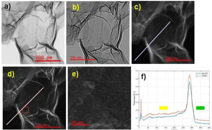
Figure 1 shows conventional a) and HFPP b) images of the graphene film at 50kx
magnification. The contrast in a) is higher in b). A thickness map obtained from logarithm of the ratio between elastic and inelastic electrons is shown in c) for data obtained without HFPP [2]. A HFPP-EFTEM thickness map obtained by the same log ratio method of zero-loss filtered and unfiltered HFPP images is shown in d). e) shows a HFPP-EFTEM thickness map obtained from the area marked by the red rectangle in d) at 300 kx magnification. The maximum thickness variation in e) is about 0.06 inelastic mean free path λ1. A EFTEM thickness map without HFPP over the same are as in e) did not yield interpretable data and was difficult to align due to presence of fringes arising from spherical aberration. Profiles along the lines indicated in c) and d), are shown in f). The upper profile in e) corresponds to the HFPP thickness map (red, dashed) from d) and the lower (blue, solid) profile to a thickness map without HFPP, derived from c). The HFPP-EFTEM thickness map appears to provide more spatial resolution that the standard
EFTEM thickness map and thinner contamination islands can be observed in the HFPP-EFTEM map more clearly than in the standard EFTEM map. The profiles in f) indicate that the addition of the HFPP in the beam for the log-ratio EFTEM thickness mapping results in addition of ~ 0.04 inelastic mean free paths λ across the field of view. The features in the HFPP-EFTEM thickness map appears to be more localized than in EFTEM thickness map without HFPP. Taking into account the known thickness of the carbon HFPP of ~13 nm, the 0.04 λ2 implies ~0.4 mrad collection angle for an object placed in the objective aperture plane rather than in sample plane.
Assuming an inelastic mean free path λ1 = 114 nm for a 200 keV beam in carbon at the sample plane (100 mrad collection angle adequate for no objective aperture), the estimated thickness in the sample region is 17.6±0.5 nm in HFPP-EFTEM (marked with yellow band in f) and 13.5±0.5 nm from the standard EFTEM thickness map.
842
doi:10.1017/S1431927617004871
Microsc. Microanal. 23 (Suppl 1), 2017 © Microscopy Society of America 2017
https://www.cambridge.org/core/terms. https://doi.org/10.1017/S1431927617004871
We have also been able to utilize HFPP-EFTEM imaging for plasmon-energy observation of Ge layers in Si single crystal MAGICALTM sample (not shown) suggesting that HFPP-EFTEM may be suitable for chemical mapping in a TEM. The log-ratio EFTEM thickness mapping method appears to yield higher spatial and thickness resolution than the standard EFTEM log-ratio thickness mapping without HFPP in the electron beam.
[1] M. Malac et. al., Ultramicroscopy 118 (2012), p. 77.
[2] R. F. Egerton, EELS in the TEM 2nd ed., Springer Verlag, 2011.
[3] Support of NINT and JEOL USA Inc. is acknowledged. The work was made possible by close collaboration with team at JEOL Ltd. Dr. Y. Okura, Dr. I. Ishikawa, Y. Konyuba and Dr. Hosogi.
Figure 1 a) Zero-loss filtered BFTEM image b) Zero-loss filtered HFPP image c) standard EFTEM thickness map d) HFPP-EFTEM thickness map. a) to d) were collected at 50kx nominal magnification..e) HFPP-EFTEM thickness map of region marked with red square in d) at 300kx nominal magnification. f) thickness profiles from c) and d) in units of inelastic mean free path on y axis and position along the profile in nm on x axis. The region in yellow and green were used to evaluate the thickness difference between the HFPP-EFTEM and standard EFTEM thickness maps in sample and vacuum respectively. The region marked in yellow in f) corresponds to a flat region of the sample while the region marked in green corresponds to vacuum in the bottom left corner of c) and d). The scale bar is 200 nm in a) to d) and 20 nm in e).
843 Microsc. Microanal. 23 (Suppl 1), 2017
https://www.cambridge.org/core/terms. https://doi.org/10.1017/S1431927617004871