HAL Id: hal-02356886
https://hal.archives-ouvertes.fr/hal-02356886
Submitted on 9 Nov 2019
HAL is a multi-disciplinary open access
archive for the deposit and dissemination of
sci-entific research documents, whether they are
pub-lished or not. The documents may come from
teaching and research institutions in France or
abroad, or from public or private research centers.
L’archive ouverte pluridisciplinaire HAL, est
destinée au dépôt et à la diffusion de documents
scientifiques de niveau recherche, publiés ou non,
émanant des établissements d’enseignement et de
recherche français ou étrangers, des laboratoires
publics ou privés.
AlGaN/GaN High Electron Mobility Transistors with
Ultra -Wide Bandgap AlN buffer
I Abid, R Kabouche, M. Zegaoui, C. Bougerol, R. Comyn, Y. Cordier, F.
Medjdoub
To cite this version:
I Abid, R Kabouche, M. Zegaoui, C. Bougerol, R. Comyn, et al.. AlGaN/GaN High Electron Mobility
Transistors with Ultra -Wide Bandgap AlN buffer. 43rd Workshop on Compound Semiconductor
Devices and Integrated Circuits, WOCSDICE 2019, Jun 2019, Cabourg, France. �hal-02356886�
AlGaN/GaN High Electron Mobility Transistors with Ultra -Wide Bandgap AlN buffer
I. Abid1*, R. Kabouche1, M. Zegaoui1, C. Bougerol2, R.Comyn3, Y. Cordier3, F. Medjdoub1*
1
CNRS-IEMN, UMR8520, Av. Poincaré, 59650 Villeneuve d'Ascq, France 2
Univ. Grenoble-Alpes, CNRS-Institut Néel, 25 av. des Martyrs, 38000 Grenoble, France
3 Univ. Côte d’Azur, CNRS, CRHEA, rue Bernard Grégory, 06560 Valbonne, France
*Email: [email protected]; [email protected]
Introduction
AlGaN/GaN high-electron-mobility transistor (HEMT) grown on silicon substrate is a promising device for cost-effective high-power and high-voltage electronic applications. In these devices, the breakdown voltage is basically limited by the total buffer thickness. In order to reach higher performances, a new generation of material system is required. In this frame, the ultra-wide-bandgap (UWBG) material AlN (6.2eV) that has a much larger bandgap than GaN (3.4eV) could enable the next leap forward in power electronics performance. Furthermore, AlN material represents the ideal back barrier for high voltage applications due to its large electrical breakdown field and high thermal conductivity. In turn, the AlN buffer can potentially not only boost the breakdown voltage owing to its wider bandgap while benefiting from an enhanced thermal dissipation as compared to GaN-based devices but also allow increasing the electron confinement in the transistor channel.
Experimental
In this paper, we present the fabrication and the DC / high voltage characteristics of two structures including thin and thick channels AlGaN/GaN HEMT on AlN buffer grown on sapphire. Lateral buffer breakdown voltage assessment reveals a remarkable breakdown field of 5 MV/cm for short contact distances in the case of the sub-10 nm channel heterostructure, which is far beyond that of GaN-based material system. Furthermore, fabricated transistors are fully functional with low leakage current and low on-resistance.
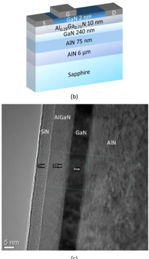
The two heterostructures consist in the regrowth of an AlN buffer layer by ammonia-MBE on a 6 µm thick AlN templates on sapphire substrates (Fig. 1).
(a)
(b)
(c)
Fig. 1.Schematic cross-section of AlGaN/GaN HEMT,
(a) thin channel structure 1, (b) thick channel structure 2 (c) and TEM of structure 1.
For the first structure, this is followed by a thin GaN channel of 8 nm and a 10 nm AlGaN barrier with a high aluminum content (90%) capped with a 7 nm in-situ SiN layer. For the second structure, a 240 nm thick GaN channel has been grown with a 10 nm AlGaN barrier (29% Al) capped with a 2 nm GaN layer. The 2DEG properties have been measured on a Van der Pauw pattern resulting in a sheet carrier density of 1.9x1013 cm-2 and an electron mobility of 200 cm²/V.s for the first structure. The rather low mobility can be attributed to the thin channel and/or to the high Al content into the barrier layer. The second structure shows a charge density of 1.1x1013 cm-2 and an electron mobility slightly higher than 1500 cm²/V.s.
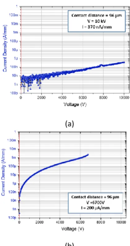
Significant lateral buffer breakdown voltage up to 10 kV has been measured on isolated ohmic contacts for large distances above 90 µm on the thin channel heterostructure (Fig. 2).
(a)
(b)
Fig. 2.Lateral breakdown voltage on 96 µm contact distance for (a) thin channel structure 1, (b) thick channel structure 2. The very high blocking voltage and the low leakage current show that the heterostructure does not suffer from any parasitic conduction as full depletion down to the sapphire substrate occurs. Interestingly, a remarkable breakdown field of 5 MV/cm is observed for short distances with for instance more than 1000 V for a 2 µm contact distance (Fig. 3). The thick channel structure delivers much lower breakdown voltage for the same contact distances. This is even more pronounced
for a
2 µm contact distance with only 270V against more than 1 kV for the thin channel structure. As it could be expected, the breakdown field of less than 2 MV/cm is limited by the thick GaN channel layer in this case.
. (a) (b)
Fig. 3. Lateral breakdown voltage on 2 µm contact distance, (a) structure 1, (b) structure 2.
It appears that the breakdown mechanism is not limited by the GaN channel when using a sub-10 nm thickness enabling to benefit from the AlN bandgap for short contacts distances. This paves the way for short AlN-based devices delivering low on-resistances above 1 kV voltage range. Thin channel Thick channel 0 20 40 60 80 100 0 2000 4000 6000 8000 10000 L a te ra l b k (V) Distance (µm)
Fig. 4. Lateral breakdown voltage for various isolated contact distances for the two structures.
Electrical characterizations were carried out on transistors with gate width/length = 50µm/1.5µm and gate-to-drain spacing (LGD) varied from 2 to 40µm. For
the various transistor designs from the thin channel structure, the off-state leakage current at VDS = 4V is
around 200 nA/mm and the static on-resistance RON
scales as expected with LGD to reach values below 15
mΩ.cm2 for a 5 µm distance.
Fig. 5. DC characteristics of AlN-based transistors with different gate drain distances for the structure 1. Despite rather poor ohmic contacts for the thick channel structure, the off-state leakage current at VDS = 4V is
below 100 µA/mm and the static on-resistance RON
scales as expected with LGD to reach values below 12
mΩ.cm2 for a 8 µm distance.
Fig. 6.DC characteristics of AlN-based transistors with different gate drain distances for the structure 2.
Conclusions
This work show that ultrathin channel AlN-based transistors could provide low on-resistances with significantly higher breakdown field far beyond the theoretical limits of GaN-based devices. Indeed, 2-terminal lateral breakdown measurements revealed a remarkable breakdown field of 5 MV/cm with more than 1000 V for a 2 µm contact distance. Furthermore, large contact distances (> 90 µm) enabled a blocking voltage above 10 kV with less than 0.5 µA/mm leakage current, reflecting the absence of parasitic conduction during the depletion down to the sapphire substrate. The rather limited electron mobility in the 2DEG can still be further improved by optimizing the device design and the growth interface quality.
ACKNOWLEDGMENT: This work is supported
by the French RENATECH network and the French National grant ANR project BREAKUP (ANR-17-CE05-0013).