HAL Id: hal-02929061
https://hal.archives-ouvertes.fr/hal-02929061
Submitted on 11 Dec 2020
HAL is a multi-disciplinary open access
archive for the deposit and dissemination of sci-entific research documents, whether they are pub-lished or not. The documents may come from teaching and research institutions in France or abroad, or from public or private research centers.
L’archive ouverte pluridisciplinaire HAL, est destinée au dépôt et à la diffusion de documents scientifiques de niveau recherche, publiés ou non, émanant des établissements d’enseignement et de recherche français ou étrangers, des laboratoires publics ou privés.
Filippo Giannazzo, Giuseppe Greco, Emanuela Schilirò, Raffaella Lo Nigro,
Ioannis Deretzis, Antonino La Magna, Fabrizio Roccaforte, Ferdinando
Iucolano, Sebastiano Ravesi, Eric Frayssinet, et al.
To cite this version:
Filippo Giannazzo, Giuseppe Greco, Emanuela Schilirò, Raffaella Lo Nigro, Ioannis Deretzis, et al.. High-Performance Graphene/AlGaN/GaN Schottky Junctions for Hot Electron Transistors. ACS Applied Electronic Materials, American Chemical Society, 2019, 1 (11), pp.2342-2354. �10.1021/ac-saelm.9b00530�. �hal-02929061�
This document is confidential and is proprietary to the American Chemical Society and its authors. Do not copy or disclose without written permission. If you have received this item in error, notify the sender and delete all copies.
High performance graphene/AlGaN/GaN Schottky junctions for hot electron transistors
Journal: ACS Applied Electronic Materials Manuscript ID el-2019-005304.R1
Manuscript Type: Article Date Submitted by the
Author: 09-Oct-2019
Complete List of Authors: Giannazzo, Filippo; Istituto per la Microelettronica e Microsistemi Consiglio Nazionale delle Ricerche,
Greco, Giuseppe; Istituto per la Microelettronica e Microsistemi Consiglio Nazionale delle Ricerche,
Schilirò, Emanuela; Istituto per la Microelettronica e Microsistemi Consiglio Nazionale delle Ricerche
Lo Nigro, Raffaella; Istituto per la Microelettronica e Microsistemi Consiglio Nazionale delle Ricerche,
Deretzis, Ioannis; Istituto per la Microelettronica e Microsistemi Consiglio Nazionale delle Ricerche,
La Magna, Antonino; Istituto per la Microelettronica e Microsistemi Consiglio Nazionale delle Ricerche,
Roccaforte, Fabrizio; Istituto per la Microelettronica e Microsistemi Consiglio Nazionale delle Ricerche,
Iucolano, Ferdinando; STMicroelectronics Branch of Catania Ravesi, Sebastiano; STMicroelectronics Branch of Catania FRAYSSINET, Eric; CRHEA,
Michon, Adrien; Université Côte d’Azur, CNRS, CRHEA Cordier, Yvon; Université Côte d’Azur, CNRS, CRHEA
High performance graphene/AlGaN/GaN Schottky junctions for hot electron transistors
Filippo Giannazzo1*, Giuseppe Greco1, Emanuela Schilirò1, Raffaella Lo Nigro1, Ioannis Deretzis1,
Antonino La Magna1, Fabrizio Roccaforte1, Ferdinando Iucolano2, Sebastiano Ravesi2, Eric
Frayssinet3, Adrien Michon3, Yvon Cordier3
1 Consiglio Nazionale delle Ricerche – Istituto per la Microelettronica e Microsistemi (CNR-IMM),
Strada VIII, n. 5 Zona Industriale, 95121 Catania, Italy
2 STMicroelectronics, Stradale Primosole 50, Zona Industriale, 95121 Catania, Italy
3 Université Côte d’Azur, CNRS, CRHEA, Rue Bernard Grégory, 06560 Valbonne, France
E-mail: [email protected]
Abstract
The electronic properties of the graphene (Gr) Schottky junction with an Al0.22Ga0.78N/GaN
heterostructure on silicon have been investigated, both experimentally and using ab-initio DFT calculations. A peculiar high n-type doping (1.1×1013 cm-2), observed for Gr in contact with AlGaN,
was explained by the combined effect of Fermi level pinning by AlGaN surface states and charge transfer. Spatially uniform current injection across the Gr/AlGaN/GaN heterojunction was revealed by nanoscale resolution conductive atomic force microscopy (CAFM) analyses. Furthermore, a Gr/AlGaN/GaN Schottky diode with excellent rectifying behavior has been demonstrated and used as the key building block for a hot electron transistor (HET) with a 10 nm Al2O3 base-collector barrier.
Thanks to the highly efficient hot electron injection from the AlGaN/GaN emitter, this transistor exhibits high on-state current density (JC,ON1 A/cm2), high-on state over off-state current density
ratio (JC,ON/JC,OFF106)anda common-base current gain 0.15, solely limited by the high Al2O3 base
collector barrier. The excellent performances of the Gr/AlGaN/GaN Schottky junction represent an important step towards the development of a HET technology compatible with the state-of-the-art GaN high electron mobility transistors.
Keywords: Graphene, GaN, hot electron transistor, conductive atomic force microscopy,
heterostructures 1. Introduction 3 4 5 6 7 8 9 10 11 12 13 14 15 16 17 18 19 20 21 22 23 24 25 26 27 28 29 30 31 32 33 34 35 36 37 38 39 40 41 42 43 44 45 46 47 48 49 50 51 52 53 54 55 56 57 58 59 60
One of the main challenges in modern electronics is the development of transistors able to operate at frequencies in the terahertz (THz) range, i.e., the electromagnetic spectrum range separating millimeter wave electronics from photonics, which is strategic for application areas like communications, medical diagnostics and security. Currently, high electron mobility transistors (HEMTs), based on the field-effect modulation of the lateral current transport in III-V semiconductor heterostructures, are the main devices for such applications, with operating frequencies exceeding 1 THz for ultra-scaled channel geometry [1,2,3,4,5]. However, further improvements of HEMT’s performances (especially their available output power) will be limited by the technological and physical issues related to lateral scaling of the channel. In this context, two dimensional (2D) semiconductors are currently explored as replacement of traditional semiconductors for ultra-scaled lateral field effect transistors with superior electrostatic gate control [6,7,8].
As an alternative to lateral field effect transistor, vertical devices can represent a solution for high frequency applications. In this context, the hot electron transistor (HET), based on the transversal ballistic transport of hot electrons through an ultra-thin base layer, has been proposed from a long time as potential candidate to operate in the THz frequency range [9,10,11,12]. It is a unipolar majority carriers vertical device, consisting of three terminals (emitter, base and collector) separated by an emitter-base and base-collector barriers. Hot electrons (i.e., electrons with energy larger than the Fermi energy of carriers in the base) are injected from the emitter to the base terminal under forward base-to-emitter polarization. For a base thickness lower than the electron mean free path, most of these hot carriers transit through the base without energy loss, and can reach the collector terminal after overcoming the base-collector filtering barrier modulated by the collector bias.
In spite of its interesting working principle, the practical implementation of this device concept has been hindered for long time by the difficulty of fabricating a high quality ultra-thin base layer using conventional growth processes, which typically suffer of increased interface roughness and degraded transport properties for very thin (<5 nm) conducting films. Recently, the appearance of two-dimensional (2D) materials provided new solutions for the implementation of high-performance HETs [13,14]. In particular, graphene (Gr) has been proposed as an ideal base material, as it combines monoatomic thickness, enabling ballistic electron transit in the transversal direction, with excellent in-plane transport properties (high mobility, from 103 up to 105 cm2V-1s-1, and very low resistivity),
[15,16,17]. Theoretical studies have predicted excellent high-frequency performances, with a cut-off frequency (fT) up to several terahertz, for Gr base HETs (GBHET) [18,19,20,21,22,23].
Besides the ultra-thin base, an emitter-base barrier allowing efficient hot electrons injection (either by thermionic emission over the barrier or by tunneling through the barrier) is a key element for the implementation of the HET device. In the first prototypes of GBHETs, the emitter-base barrier was 3 4 5 6 7 8 9 10 11 12 13 14 15 16 17 18 19 20 21 22 23 24 25 26 27 28 29 30 31 32 33 34 35 36 37 38 39 40 41 42 43 44 45 46 47 48 49 50 51 52 53 54 55 56 57 58 59 60
represented by a nanometer-thin SiO2 tunneling barrier thermally grown on a n+-doped Si substrate
(working as the electrons emitter), while the base collector-barrier was obtained with a high-k insulator (Al2O3 or HfO2) deposited on Gr [24,25]. However, these demonstrators suffered of a very
poor injected current density (10-4-10-3 A/cm2) and a high threshold voltage (V
th5 V), mainly due
to the large electron affinity difference between Si and SiO2. Significant improvements in the current
injection efficiency have been obtained by a careful choice of the emitter and emitter-base barrier materials and the improvement of the interfaces quality. As an example, replacing SiO2 with a higher
electron affinity insulator (such as HfO2) grown on Si resulted in a reduced threshold voltage and a
higher injected current, whereas further improvement in the injection efficiency was obtained by tunnel barrier engineering, e.g., using a TmSiO/TiO2 bilayer [26].
The early GBHETs demonstrators were developed on a Si substrate, with the aim of integrating these new devices with conventional CMOS technology. More recently, the possibility of implementing GBHETs with high on-state current by the integration of Gr with group III- Nitride semiconductors has been considered [27,28,29]. In particular, thin films of AlN or AlxGa1-xN,
epitaxially grown on GaN by MOCVD or MBE, resulted excellent emitter-base barriers, due to their superior structural quality as compared to oxide layers. Further advantages of these material systems are the presence of high density (1013 cm-2) two dimensional electron gas (2DEG) at the Al
xGa 1-xN/GaN interface, working as the hot electrons emitter, as well as the possibility of tailoring the
conduction band discontinuity between AlxGa1-xN and GaN by the Al content. Very efficient current
injection by Fowler-Nordheim (FN) tunneling mechanism has been recently demonstrated in the case of Gr junctions with thin barriers of AlN (3 nm) [29] or Al-rich Al0.65Ga0.35N (4.7 nm) [30] grown on
n+ doped GaN. High quality bulk GaN substrates with dislocations density <105 cm-2 have been used
as substrates to grow these very thin barrier layers with a sufficient quality to avoid leakage current through defects. Actually, the high cost of these substrates will probably limit the widespread development of the AlN/GaN emitter in the near future.
On the other hand, AlxGa1-xN/GaN heterostructures with a thicker (20 -25 nm) AlGaN barrier
layer with lower Al content (x=0.2 - 0.3), typically grown on sapphire, Silicon Carbide (SiC), or Silicon (Si) are widely employed in the GaN HEMTs technology for radio-frequency (RF) applications. The development of Gr-base HETs on these heterostructures can be highly interesting, as it can open the way to the integration of two different high frequency transistor technologies on the same platform.
To date, only few literature studies [31,32,33] reported on such systems, showing how the vertical current transport at Gr/AlxGa1-xN/GaN interface depends on the composition (i.e., the Al content)
3 4 5 6 7 8 9 10 11 12 13 14 15 16 17 18 19 20 21 22 23 24 25 26 27 28 29 30 31 32 33 34 35 36 37 38 39 40 41 42 43 44 45 46 47 48 49 50 51 52 53 54 55 56 57 58 59 60
[33], the microstructure (dislocation density) [31] of the AlGaN barrier layer, as well as on Fermi level pinning effects at Gr/AlGaN interface [27].
In this work, the electronic properties of the Gr junction with an optimized quality AlxGa1-xN/GaN
heterostructure (with x=0.22, tAlGaN=21 nm) on Si(111) have been investigated in details, both
experimentally and using ab-initio calculations. A peculiar high n-type doping (1.1×1013 cm-2) was
measured for Gr in contact with the AlGaN, which was explained at atomistic level by the combined effect of Fermi level pinning by AlGaN surface states and charge transfer. Nanoscale resolution conductive atomic force microscopy (CAFM) analyses revealed a highly uniform current injection across the Gr/AlGaN/GaN heterojunction. A Gr/AlGaN/GaN Schottky diode with excellent rectifying behavior has been demonstrated, where the current injection under forward polarization is ruled by thermionic emission above the AlGaN barrier. This diode was used as the key building block for a HET with a 10 nm Al2O3 base-collector barrier. Thanks to the highly efficient hot electron
injection from the AlGaN/GaN emitter, this transistor exhibits high on-state current density of JC,ON1
A/cm2andsix decades modulation of J
C by the base-emitter bias. The common base current gain
reached a value of 0.15, only limited by the high Al2O3 base collector barrier.
The excellent performances of Gr Schottky junction with the AlGaN/GaN heterostructure on Si represent an important step towards the development of a hot electron transistors technology compatible with the state-of-the-art GaN HEMTs production.
2 Results and Discussion
2.1 Structural and electrical properties the heterojunctions
High quality AlxGa1-xN/GaN heterostructures grown by metal organic chemical vapor deposition
(MOCVD) on Si(111) wafers were the starting material for the fabrication of the Gr/AlGaN/GaN Schottky junctions object of this investigation. Fig.1(a) reports a schematic cross section of the Nitride structure on the Si(111) substrate, including a sequence of different layers (1.4 µm GaN / 20 nm AlN / 700 nm GaN / 200 nm AlN) properly designed to minimize the threading dislocations density reaching the topmost AlGaN/GaN heterostructure. A preliminary assessment of the epilayers crystalline quality was obtained by X-ray diffraction patterns, which confirmed the Al mole fraction in the AlxGa1-xN barrier (x=0.22) and the thickness dAlGaN=21 nm. Fig.1(b) shows a high-resolution
cross-sectional transmission electron microscopy of the topmost region of the heterostructure, confirming the atomically sharp and high crystalline quality of the AlGaN/GaN interface. Fig.1(c) shows a tapping mode atomic force microscopy (AFM) image of the AlGaN surface on 5 m × 5 m scan area, which reveals a smooth morphology with a root mean square (RMS) roughness of 0.45 nm. Small pits present on the sample surface can be associated to threading dislocations with a surface 3 4 5 6 7 8 9 10 11 12 13 14 15 16 17 18 19 20 21 22 23 24 25 26 27 28 29 30 31 32 33 34 35 36 37 38 39 40 41 42 43 44 45 46 47 48 49 50 51 52 53 54 55 56 57 58 59 60
density lower than 2×10⁹/cm², in agreement with the full width at half maximum of X-ray diffraction
peaks at 620 arcsec for GaN (002) and 1090 arcsec for GaN (302) reflections. Finally, a preliminary electrical characterization of the as-grown AlGaN/GaN heterostructure was carried out by capacitance-voltage (C-V) measurements with a mercury (Hg) probe. Fig.1(d), left vertical axis, shows a C-V curve acquired at a frequency of 20 kHz by negative biasing the Hg Schottky contact (from 0 to -8V) to deplete the 2DEG at the AlGaN/GaN interface. The height of the capacitance plateau starting from V=0V is related to the AlGaN thickness dAlGaN according to the relation
C(0)=0AlGaN/dAlGaN (being 0 the absolute permittivity and AlGaN=9.39 the relative permittivity of
AlxGa1-xN with x=0.22 [34]). The 2DEG pinch-off voltage is -4.5V. The blue line (right vertical
axis in Fig.1(d)), obtained by integration of the C-V curve, represents the 2DEG charge density ns
modulated by the applied bias. In particular, a carrier density of about 9×10¹²/cm² at zero bias was
estimated. The 2DEG sheet resistance Rsh=4365 /sq was obtained by electrical measurements of
transmission line model (TLM) test patterns fabricated on the heterostructure. By combining this Rsh
value with the ns value from C-V analyses, a carrier mobility =(q ns Rsh)-11600 cm2V-1s-1 was
estimated for the 2DEG at AlGaN/GaN interface.
Fig.1 (a) Schematic cross section of the multilayer structure grown on the Si(111) substrate. (b)
High-resolution cross-sectional TEM of the topmost AlGaN/GaN heterostructure in the multilayer. (c) AFM image of the as-grown AlGaN surface (5 m × 5 m scan area). (d) Hg probe C-V measurement 3 4 5 6 7 8 9 10 11 12 13 14 15 16 17 18 19 20 21 22 23 24 25 26 27 28 29 30 31 32 33 34 35 36 37 38 39 40 41 42 43 44 45 46 47 48 49 50 51 52 53 54 55 56 57 58 59 60
(black line, left vertical axis) of the AlGaN acquired at a frequency of 20 kHz by negative biasing the Hg Schottky contact from 0 to -8V. The blue line (right vertical axis) is the 2DEG charge density ns
modulated by the bias.
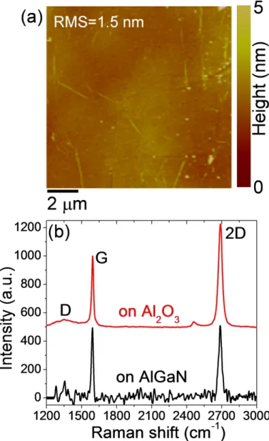
Monolayer (1L) graphene (Gr) grown by chemical vapor deposition (CVD) on copper foils was transferred onto the AlGaN barrier layer (see the “Materials and Methods” section). A typical AFM image of Gr onto AlGaN is reported in Fig. 2(a), showing a uniform coverage of the AlGaN surface by the Gr membrane without pinholes and cracks The higher RMS roughness with respect to bare AlGaN (Fig.1(c)) is mainly related to the presence of wrinkles, i.e., nanometer height corrugations of the Gr membrane. Some of these features are present in Gr starting from the CVD growth [35], whereas part of them are introduced during transfer procedure. The impact of wrinkles on the vertical current injection in the Gr/AlGaN/GaN heterostructure will be discussed later on in this paper. Fig.2(b) shows two representative Raman spectra of 1L Gr transferred onto the AlGaN surface and on a standard insulating substrate (Al2O3 on Si), used as a reference. The two spectra, normalized to
the G peak intensity, exhibit a very weak defects-related D peak, indicating a high structural quality of Gr. While Gr onto Al2O3 shows a 2D over G peak intensity ratio I2D/IG1.3, consistent with the
typically reported values for 1L Gr with low unintentional p-type doping [36], a significantly lower ratio, I2D/IG1, was found for 1L Gr residing onto AlGaN. Such a difference can be ascribed to a
higher doping of Gr in contact with this Nitride semiconductor substrate. The type of doping and the carrier density will be further elucidated in the following by electrical measurements on device test structures. 3 4 5 6 7 8 9 10 11 12 13 14 15 16 17 18 19 20 21 22 23 24 25 26 27 28 29 30 31 32 33 34 35 36 37 38 39 40 41 42 43 44 45 46 47 48 49 50 51 52 53 54 55 56 57 58 59 60
Fig. 2 (a) Typical AFM image of monolayer (1L) Gr on the AlGaN surface, showing a uniform
coverage without pinholes and cracks. (b) Representative Raman spectra of 1L Gr onto AlGaN and on an Al2O3 insulating substrate, used as a reference.
Fig.3(a) and (b) schematically illustrate two top-gated Gr field effect transistors (GFETs) with the Gr channel residing onto the AlGaN/GaN heterostructure and on the Al2O3/Si substrate (used as a
reference). In both cases, a thin (10 nm) Al2O3 top gate dielectric was deposited on Gr by atomic layer
deposition (ALD) [37]. The transfer characteristics (ID-VG) measured on the two transistors with an
applied VDS=0.1 V are reported in Fig.3(c) and (d). A slight positive shift of the neutrality point
(VNP=0.7 V) is observed for the Gr FET onto Al2O3, indicating a small p-type doping of Gr, typically
due to resist contaminations or ambient humidity. On the contrary, for the Gr FET onto AlGaN, a large negative shift of the neutrality point (VNP=-2V) is found. This indicates a high n-type doping of
Gr, which over-compensates the contaminations related unintentional p-type doping. An electron density ngr=1.1×1013 cm-2 was estimated for Gr onto AlGaN according to the relation
ngr=Cox(WM-Wgr-VNP)/q, (Eq.1)
where WM=5 eV is the workfunction of the Nickel top-gate metal, Wgr=4.5 eV is the theoretical
workfunction for charge neutral Gr, Cox is the top gate oxide capacitance per unit area (Cox=0ox/tox,
with ox8 the Al2O3 relative dielectric constant [37] and tox=10 nm the oxide thickness). Statistical
analysis has been carried out on a set of 10 top-gated Gr FETs onto AlGaN. From the average value of the neutrality point position (<VNP>=-2 V) and its standard deviation (VNP=0.1 V), the mean
carrier density (<ngr>=1.1×1013 cm-2) of the n-type doped Gr onto AlGaN and its variability
(ngr=0.4×1012 cm-2) were obtained.
This electrons density corresponds to a positive shift of the Fermi level from the Dirac point EF
-ED0.39 eV, evaluated according to the relation:
EF,gr-ED=ħvF(ngr)1/2/q (Eq.2).
The field effect mobility values of electrons for Gr onto AlGaN (and holes for Gr on Al2O3) was
estimated from the slope dID/dVG of the transfer characteristic, according to the relation
=L/(WCoxVDS)dID/dVG, where L=50 m and W=150 m are the channel length and width,
respectively, and VDS=0.1 V the drain bias. The lower carrier mobility (e=620 cm2V-1s-1) for Gr onto
AlGaN with respect to Gr onto Al2O3 (h=1120 cm2V-1s-1) can be ascribed to the enhanced Coulomb
scattering due to the high n-type doping of Gr. 3 4 5 6 7 8 9 10 11 12 13 14 15 16 17 18 19 20 21 22 23 24 25 26 27 28 29 30 31 32 33 34 35 36 37 38 39 40 41 42 43 44 45 46 47 48 49 50 51 52 53 54 55 56 57 58 59 60
Fig.3 Schematic illustration of two top gated FETs with Gr residing on the AlGaN/GaN
heterostructure (a) and on an Al2O3/Si substrate (b). Transfer characteristics measured on the Gr FET
supported by AlGaN/GaN (c) and Al2O3/Si (d).
2.2 Ab-initio DFT calculations
In the following, ab-initio density functional theory (DFT) calculations of the Gr/Nitride semiconductors interface were carried out, to elucidate the atomistic origin of the high n-type doping of Gr. Due to difficulty of simulating the interface with an AlxGa1-xN alloy, AlN was adopted as a
model system in our computational analysis [38]. We initially studied the structural and electronic properties of the interface between an ideally Al-terminated AlN(0001) surface and Gr. Fig. 4(a) shows the structural characteristics of this interface upon atomic relaxation. The Gr sheet remains practically flat and maintains a distance of 3.4 Å from the topmost Al atoms on the AlN surface. Such structural decoupling indicates that the heterostructure bonding is intrinsically low. Fig.4(b) shows the calculated band structure of this system, after unfolding the bands of each part of the heterojunction (i.e., Gr and the AlN substrate) to the respective primitive Brillouin zones. The Gr-related bands, reported as red lines, show the unperturbed Dirac cone standing at the K point of the hexagonal Brillouin zone of Gr. The AlN-related bands are indicated as green lines, whereas the blue 3 4 5 6 7 8 9 10 11 12 13 14 15 16 17 18 19 20 21 22 23 24 25 26 27 28 29 30 31 32 33 34 35 36 37 38 39 40 41 42 43 44 45 46 47 48 49 50 51 52 53 54 55 56 57 58 59 60
lines represent the calculated contribution of the AlN(0001) surface only. The principal characteristic from an electronic viewpoint is the unusually high shift of the Fermi level above the Dirac point (EF
-ED 0.73 eV), corresponding to an electron density of ngr3.9×1013 cm-2. Furthermore, looking at the
positioning of the Fermi level with respect to the AlN, it can be observed that it is “pinned” at the conduction band of the AlN surface (blue line). Besides this Fermi level pinning effect, which is intrinsic of the Al termination of the AlN surface, another possible mechanism contributing to the unusually high n-type doping of Gr can be represented by the charge transfer from the less electronegative Al atoms towards the C atoms of Gr. As a matter of fact, these charge transfer phenomena are expected to depend on the distance between Gr and the AlN(0001) surface. Hence, to evaluate the relative weight of the two mechanisms, we performed single-point energy evaluations by fixing the atomic positions of an ideal Gr/AlN(0001) interface while progressively varying the interface distance from the equilibrium value (3.4 Å) up to 6.4 Å. Fig.4(c) – upper panel illustrates the calculated shift of the Gr Fermi level with respect to the Dirac point (EF-ED) as a function of the
distance and the corresponding changes in the Gr doping (lower panel). It can be observed how the initial high n-type doping rapidly decreases from the value of 3.9×1013 cm-2 at the equilibrium
distance to 1×1013 cm-2 at 3.9 Å, and it reaches a saturating value of 0.3×1013 cm-2 for distances
above 4.4 Å. While the decreasing doping values are due to charge transfer from the Al atoms, the saturation value can be ascribed to the above discussed Fermi level pinning effect.
Fig.4: (a) Equilibrium structure and (b) energy bands for an ideal AlN(0001)/Gr interface. The bands
for the different parts of the heterostructure have been unfolded to the corresponding first Brillouin zones of Gr (red points) and AlN (green points). The contribution of the topmost Al atoms of the AlN surface is shown as blue points. (c) Shift of the Fermi level from the Gr Dirac point (EF-ED) and
corresponding electron density (ngr) for a Gr/AlN(0001) interface as a function of the Gr-AlN
distance.
These theoretical results, obtained in the case of an ideally Al-terminated AlN surface and Gr, indicate that the high n-type doping of Gr is an intrinsic property of the Gr/AlN interface. We extended the simulations work to consider also some cases of non-ideal AlN surfaces. Fig.5(a)-upper panel, shows 3 4 5 6 7 8 9 10 11 12 13 14 15 16 17 18 19 20 21 22 23 24 25 26 27 28 29 30 31 32 33 34 35 36 37 38 39 40 41 42 43 44 45 46 47 48 49 50 51 52 53 54 55 56 57 58 59 60
the relaxed configuration of Gr on a Al-poor surface with Al vacancies in a (2×2) surface pattern. In this case, Gr stands closer to the AlN surface (the Al-C distance is just 2.6 Å here) and shows a small corrugation. Both features indicate a stronger interface coupling with respect to the ideal case. Fig. 5(a)-lower panel shows the unfolded band structure of this system. Here, the surface-induced Al band is absent, due to the high concentration of Al defects, whereas numerous defect-states appear inside the band gap. The Gr bands are slightly perturbed near the Dirac point, and an even higher n-type doping is found (EF-ED1.15 eV corresponding to n9.7×1013) due to the closer Al-C distance and
the higher charge transfer from the Al atoms towards Gr.
Finally, we also simulated the effect of a partial oxidation of the AlN surface, that can be found experimentally, to understand its effect on the electronic properties of the AlN(0001)/Gr heterostructure. To this purpose, we have considered a model based on O adatoms with a (2×2) pattern over the ideal AlN surface (Fig. 5(b)-upper panel). Even in this case, the high electron doping is found to be extremely robust (Fig. 5(b)-lower panel), excluding that a partial interface oxidation can change the qualitative picture described previously.
Fig.5: Structural and electronic properties for (a) an Al-poor AlN(0001)/Gr interface and for (b) an
oxygen-rich AlN(0001)/Gr interface. The respective band structures have been unfolded to the corresponding first Brillouin zones of Gr (red points) and AlN (green points). The contribution of the topmost Al atoms (a) and the oxygen ad-atoms (b) are shown as blue points.
3 4 5 6 7 8 9 10 11 12 13 14 15 16 17 18 19 20 21 22 23 24 25 26 27 28 29 30 31 32 33 34 35 36 37 38 39 40 41 42 43 44 45 46 47 48 49 50 51 52 53 54 55 56 57 58 59 60
DFT calculations provide a picture of the origin of Fermi level pinning and high n-type doping in Gr residing on the surface of AlN(0001). These considerations can be extended to the case of Gr onto the AlGaN barrier layer object of this experimental investigation.
2.3 Electrons injection at Gr/AlGaN interface
The vertical current injection across the Gr/AlGaN/GaN heterojunction was investigated both at nanoscale, using conductive atomic force microscopy (CAFM) [39,40], and at device level on Schottky diode structures.
Fig.6(a) illustrates the setup for CAFM-based vertical current measurements [41,42,31]. In this configuration, the local current flowing vertically from Gr to the 2DEG at AlGaN/GaN interface is measured by applying a bias between the nanoscale tip scanned onto Gr and a macroscopic ohmic contact fabricated onto AlGaN. A typical current-voltage (I-Vtip) characteristic measured in this
configuration is reported in Fig.6(b). It exhibits a rectifying behavior, with negligible current at negative bias values and current onset at positive ones. Fig.6(c) and (d) show a typical morphology and the corresponding vertical current map measured with the tip scanned on the Gr membrane. Uniform current injection can be deduced from Fig.6(d), except for a local reduction of current on the wrinkles. Such effect can be ascribed to a local reduction of doping induced by the AlGaN substrate in these corrugations of the Gr membrane. This hypothesis is also supported by the results of DFT calculations for the Gr doping dependence on the distance from the AlN surface (see Fig.4(c)). Considering that wrinkles locally detach from the substrate by few nm altitude (see line profile in Fig.6(c)), those calculations indicate that the local doping of Gr can be reduced by more than one order of magnitude (down to 3×1012 cm-2) in these areas.
3 4 5 6 7 8 9 10 11 12 13 14 15 16 17 18 19 20 21 22 23 24 25 26 27 28 29 30 31 32 33 34 35 36 37 38 39 40 41 42 43 44 45 46 47 48 49 50 51 52 53 54 55 56 57 58 59 60
Fig.6 (a) Schematic illustration of the setup for vertical current measurements with CAFM. (b)
Typical current-voltage (I-Vtip) characteristic measured in the vertical configuration, showing a
rectifying behavior, with negligible current at negative bias values and current onset at positive ones. (c) Morphology and (d) vertical current map measured with the tip scanned on the Gr membrane. A linescan showing the height of a Gr wrinkle is shown in the insert of panel (c).
The vertical current injection through the Gr/AlGaN/GaN heterojunction was investigated on properly fabricated diode structures, as discussed in the Materials and Methods section. A schematic cross-section of the diode is illustrated in Fig.7(a), whereas Fig.7(b) shows a typical current-voltage characteristic measured at a temperature T=298 K. This curve exhibits an excellent rectifying behavior, with a very low current under reverse (negative) bias and a linear increase of the current (in the semilog scale) in a range of 8 decades under forward (positive) bias. To further investigate the mechanisms of current injection at this heterojunction, a temperature dependent I-V characterization has been carried out. Fig.7(c) shows a sequence of forward bias I-V curves collected at different temperatures, in the range from 298 to 448 K. A strong dependence of the current on the temperature can be observed, indicating thermionic emission as the main current injection mechanism. In order to evaluate the Schottky barrier height B of the Gr/AlGaN interface, a linear fit of the I-V curves in
Fig.7 (c) has been performed in the low bias region. The intercept on the current axis of this fit is the saturation current term Is=AA*T2exp(-qB/kT) of the thermionic emission equation I=Isexp(qV/nkT),
where A is the Schottky diode area, A* the Richardson constant, k the Boltzmann constant, q the electron charge, T the temperature and n the ideality factor. Fig.7(d) shows the semilog-scale plot of 3 4 5 6 7 8 9 10 11 12 13 14 15 16 17 18 19 20 21 22 23 24 25 26 27 28 29 30 31 32 33 34 35 36 37 38 39 40 41 42 43 44 45 46 47 48 49 50 51 52 53 54 55 56 57 58 59 60
Is/T2vs 1000/T. The Gr/AlGaN Schottky barrier height value (B=0.620.03 eV) is obtained as the
slope of the linear fit of these data. By statistical analysis of 10 different Gr/AlGaN/GaN diodes, a mean Schottky barrier height value <B>=0.64 eV with a standard deviation of 0.05 eV was
extimated.
It is worth noting that this barrier height value is much lower than the one expected according the Schottky-Mott theory for an ideal Gr/AlGaN Schottky barrier, i.e., B=Wgr-AlGaN=1.9 eV, being
Wgr=4.5 eV the workfunction of neutral graphene and AlGaN=2.6 the electron affinity for
Al0.22Ga0.78N [43]. This large discrepancy can be ascribed to a Fermi level pinning at the interface
between Gr and AlGaN, consistently with predictions of DFT calculations.
Fig.7 (a) Schematic cross-section of a Gr/AlGaN/GaN diode. (b) Current-voltage (I-V) characteristic
measured on this diode at a temperature of 25 °C, under forward and reverse polarization. (c) Sequence of forward bias I-V curves measured at different temperatures, in the range from 25 to 175 °C. For each curve, a linear fit in the low bias region has been carried out to extract the saturation current value IS. (d) Semilog-scale plot of Is/T2vs 1000/T and linear fit of the data, from which the
Gr/AlGaN Schottky barrier height value (B=0.620.03 eV) is obtained.
3 4 5 6 7 8 9 10 11 12 13 14 15 16 17 18 19 20 21 22 23 24 25 26 27 28 29 30 31 32 33 34 35 36 37 38 39 40 41 42 43 44 45 46 47 48 49 50 51 52 53 54 55 56 57 58 59 60
The Schottky barrier height at Gr/AlGaN interface is the key parameter ruling current injection in the Gr/AlGaN/GaN heterojunction diode under low forward bias polarization. However, in order to exploit this system as the base-emitter junction for a vertical hot electron transistor, an accurate modeling of the behavior of the injected current with the forward bias is necessary in a wide bias range. Looking in details to a typical I-V characteristic measured on the Gr/AlGaN/GaN diode (see Fig.8(a)), three different conduction regimes can be identified: a low and intermediate current regimes, showing linear ln(I)-V behavior with two different slopes (black and red linear fits), followed by a region of current saturation at larger bias. This saturation is due to partial drop of the forward potential on the series resistances (i.e. the contact resistances to AlGaN/GaN and to Gr, and the resistances of the access regions to the device active area) occurring at large current levels. The two linear ln(I)-V regions at different slopes are not peculiar of the Gr Schottky contact with AlGaN/GaN, as such behavior has been also observed for common metals on III-V or III-N heterostructures embedding a 2DEG [44]. Recently, Greco et al. [45] observed a similar behavior in the case of Ni/Au Schottky contacts onto AlGaN/GaN heterostructures and described it analytically considering the series combination of two Schottky diodes, the first one (the metal/AlGaN diode) ruling transport at lower bias and the second one (the 2DEG/AlGaN diode) at higher bias.
Hence, this “two-diodes model” was adapted to the specific case of the Gr/AlGaN/GaN heterojunction. Fig.8(b) illustrates the energy band diagrams of the heterojunction at different forward polarization biases. Here, B1 indicates the Schottky barrier height at the Gr/AlGaN interface (i.e.,
B previously evaluated), while B2 is the barrier of the second-diode between the 2DEG and AlGaN.
At V=0 the system is under equilibrium and the Fermi levels of Gr (EF,gr) and of the AlGaN/GaN
2DEG (EF,s) are aligned. With increasing the forward polarization bias V, the EF,s is upward shifted
with respect to EF,gr. This results in a change of the potential V across the AlGaN layer, which
decreases to zero (at flatband voltage V=VFB) and therefore inverts its sign. As illustrated in Fig.8(a),
the flatband voltage condition (VFB=0.95 V) can be identified as the intersection point between two
linear regions in the semilog scale I-V curves [45]. For 0<V<VFB, the thermionic emission current at
the Gr/AlGaN/GaN junction is ruled by the Schottky barrier B1=0.62 eVand by the ideality factor
n1=2.3, according to the equations:
, (Eq.3a) kT n qV exp I I s 1 1 1 . (Eq.3b) kT q exp T AA I * B s 1 2 1
For V>VFB, the current transport is described by the equations:
3 4 5 6 7 8 9 10 11 12 13 14 15 16 17 18 19 20 21 22 23 24 25 26 27 28 29 30 31 32 33 34 35 36 37 38 39 40 41 42 43 44 45 46 47 48 49 50 51 52 53 54 55 56 57 58 59 60
(Eq.4a)
kT n V V q exp I I FB s 2 2 2 . (Eq.4b) kT q exp T AA I ** B s 2 2 2Here, A**isthe Richardson constant for the 2DEG/GaN contact (which can be different from A* for
the Gr contact onto AlGaN), n2=2.7 is the ideality factor, and B2 is the barrier between the 2DEG
and AlGaN.
Fig.8 (a) Semilog-scale I-V characteristic of the Gr/AlGaN/GaN Schottky diode under forward bias
polarization and (b) energy band diagrams of this system for different bias conditions. 3 4 5 6 7 8 9 10 11 12 13 14 15 16 17 18 19 20 21 22 23 24 25 26 27 28 29 30 31 32 33 34 35 36 37 38 39 40 41 42 43 44 45 46 47 48 49 50 51 52 53 54 55 56 57 58 59 60
According to Fig.8(a), Eq.3a and Eq.4b give the same current value at V=VFB. Hence, by equating
the second terms of these equations, and from the band diagram in Fig.8(b) for V=VFB, the following
relation can be derived between the barrier heights B1, B2 and the saturation current values Is1, Is2:
(Eq.5)
2 1
1 2 B s s B ln I ln I q kT Noteworthy, this equation allows to evaluate B2 directly from the value of B1 (obtained from the
Richardson plot in Fig.7(d)), and by the experimental values of ln(Is1)-371 and ln(Is2)-211,
without the need of knowing the Richardson constant. The obtained value of B221725 meV is in
good agreement with the expected value (B2199 meV) according to the band diagram in Fig.8(b),
i.e.:
B2=EC-[EF,s-ECmin], (Eq.6)
where EC=297 meV is the calculated conduction band discontinuity at the AlxGa1-xN/GaN interface
for x=0.22 [34] and EF,s-ECmin=98 meV is the Fermi level position with respect to the bottom of the
quantum well. This was obtained using the expression of EF,s-ECmin for a 2DEG of Schroedinger
electrons (with parabolic dispersion relation), i.e., EF,s-ECminħ2ns/(qmeff), being ħ the reduced
Planck’s constant, meff=0.22me the electrons effective mass [34] and ns=9×1012 cm-2 the carrier
density (evaluated in Fig.1(c)).
As discussed above, the saturation regime of the ln(I)-V characteristics of the Gr/AlGaN/GaN diode at high forward bias is determined by the series resistance contributions associated to the metal/Gr and metal/AlGaN contacts, and to the access regions. A series resistance value of R=2.30.2 k was evaluated by fitting this region of the I-V curve with the function I=(V-VR)/R, reported as a blue line
Fig.8(a).
Once the key physical parameters describing the Gr/AlGaN/GaN junction have been obtained, these were employed to evaluate the energy of hot electrons (Ehe) injected by thermionic emission over the
barrier. As illustrated in the band-diagrams in Fig.8(b), for V≤VFB, electrons overcoming the barrier
have an energy Ehe=B1 (or higher). On the other hand, for V>VFB, a linear increase of Ehe= B1+V
as a function of the bias V is expected, followed by a saturation behavior due to the series resistance effect. The behavior of Ehe as a function of V in these three different regimes is reported in the insert
of Fig.8(a). 3 4 5 6 7 8 9 10 11 12 13 14 15 16 17 18 19 20 21 22 23 24 25 26 27 28 29 30 31 32 33 34 35 36 37 38 39 40 41 42 43 44 45 46 47 48 49 50 51 52 53 54 55 56 57 58 59 60
2.4 Hot Electrons Transistor
After investigating the basic properties of the Gr/AlGaN interface and modeling the current voltage characteristic of the G/AlGaN/GaN diode in the entire forward bias range, we fabricated a complete hot electron transistor (HET) structure (see the Materials and Methods section). A schematic cross-section of the HET device is illustrated in Fig.9 (a). With respect to the diode structure in Fig.7(a), it includes a thin Al2O3 film, with thickness tox=10 nm, working as the base-collector barrier. A typical
AFM morphology of the as-deposited Al2O3 on the Gr/AlGaN surface is reported in Fig.9(b),
demonstrating the uniform an conformal (i.e. pinholes-free) coverage of Gr by the insulating layer. The Al2O3 deposition was carried out using an optimized two-steps ALD process [37], which consists
of a low temperature (100 °C) deposition step for the nucleation of a uniform AlOx seed layer on the Gr surface [46], followed by a higher temperature deposition at T=250 °C. This process, initially developed for Gr transferred onto common insulating substrates [37], was demonstrated to result in a very good Al2O3 coverage of the Gr surface. More recent investigations have shown an improved
Al2O3 nucleation in the case of highly n-type doped Gr [47], which justifies the very uniform
morphology of Al2O3 onto Gr/AlGaN shown in Fig.9(b).
Fig.9(c) reports a top-view optical microscopy of the complete HET device, where the Ni/Au collector contact (C) deposited on the thin Al2O3 film, the Ni/Au pads contacting the Gr base (B) and
the alloyed Ti/Al/Ni/Au Ohmic contacts on the AlGaN/GaN emitter (E) are indicated. The device active area (100 m×100 m), i.e. the region where the emitter, base and collector are overlapped, is delimited by a red dashed line.
3 4 5 6 7 8 9 10 11 12 13 14 15 16 17 18 19 20 21 22 23 24 25 26 27 28 29 30 31 32 33 34 35 36 37 38 39 40 41 42 43 44 45 46 47 48 49 50 51 52 53 54 55 56 57 58 59 60
Fig.9 (a) Schematic cross-section of the hot electron transistor structure. (b) AFM image of the Al2O3
base-collector barrier deposited on Gr. (c) Top-view optical microscope image of the HET device.
Fig.10(a) shows the collector current density (JC) measured on the base-collector diode by applying
a positive bias ramp to the collector terminal (VCB= VC-VB from 0 to 3 V, with the base terminal
grounded, VB=0) and VBE=0 V at the emitter-base junction. The low current density values
JC1A/cm2 measured for VCB<2.2 V correspond to the leakage current across the base-collector
barrier. For VCB>2.2 V an exponential increase of the JC is observed, which was described by a
Fowler-Nordheim (FN) tunneling mechanism:
(Eq.7) CB ox CB ox CB ox ox CB C V t qh m exp t hm mV q J 3 2 8 8 3 3
with mox the electron tunneling mass for Al2O3, m the free electron mass, h the Planck’s constant and
tox=10 nm the Al2O3 thickness. Fig.10(b) shows the energy band diagrams for the Gr/AlGaN/GaN
system at equilibrium (left panel) and for high enough VCB allowing tunneling through the triangular
barrier (right panel). Noteworthy, the base-collector barrier CB depends on the collector bias VCB,
due the field effect modulation of the Gr Fermi level, and it can be expressed as: 3 4 5 6 7 8 9 10 11 12 13 14 15 16 17 18 19 20 21 22 23 24 25 26 27 28 29 30 31 32 33 34 35 36 37 38 39 40 41 42 43 44 45 46 47 48 49 50 51 52 53 54 55 56 57 58 59 60
, (Eq.8) q n q V C n v ox CB gr gr F , CB CB 0
where CB,0 is the base-collector barrier value (at VCB=0) and ngr=1.1×1013 cm-2 is Gr the electrons
density, as evaluated from the top-gated GFET characterization in Fig.3(c). By fitting the IC-VCB
characteristics with Eqs.(7)-(8), a value of CB,0=1.31 eV was obtained for mox=0.55 me [48].
Fig.10 (a) Current-voltage (JC-VCB) characteristic of the base-collector diode (for VBE=0 V) and fit
with Fowler-Nordheim tunneling model. (b) Energy band diagrams for the Gr/AlGaN/GaN system at equilibrium (left panel) and for high enough VCB allowing tunneling through the triangular barrier
(right panel).
After evaluating the key physical parameters ruling the electron transport across the base-collector barrier, the electrical characterization of the full HET structure has been performed, in order to evaluate the efficiency of hot electrons injection from the AlGaN/GaN emitter into the Gr base. Fig.11(a) shows the emitter (JE) and collector (JC) current densities measured as a function of the
emitter-base bias (VBE from 0 to 3 V) in the common base configuration (VB=0 V) and for a fixed
collector bias VCB=2V. The injected current measured at the emitter terminal (JE) exhibits an
exponential dependence on VBE, consistently with the behavior of the Gr/AlGaN Schottky diode.
The JC-VBE characteristic exhibits a turn-on voltage 1.3 V, with a low off-state current density
JC,OFF1 A/cm2 (for VBE<1.3 V) associated to the leakage current of cold electrons through the Al2O3
barrier. The exponentially increasing JC for VBE>1.3 V is associated to the current of hot electrons
3 4 5 6 7 8 9 10 11 12 13 14 15 16 17 18 19 20 21 22 23 24 25 26 27 28 29 30 31 32 33 34 35 36 37 38 39 40 41 42 43 44 45 46 47 48 49 50 51 52 53 54 55 56 57 58 59 60
injected from the emitter into the Gr base, that are able to reach the collector. By statistics on 10 different HETs, an average turn-voltage of 1.2 V with a standard deviation of 0.1 V was obtained. Thanks to the efficient hot electrons injection at the Gr/AlGaN/GaN heterojunction, an ON/OFF current density ratio JC,ON/JC,OFF106with a JC,ON=1 A/cm2 is achieved. Fig.10(b) shows the common
base current gain of the transistor, i.e. the ratio =JC/JE, which reaches values from 0.1 to 0.15 at
VBE>2V.
Theoretically, can be expressed as =B BC, where B=exp(-tGr/l) is the base efficiency (being
tGr0.35 nm the monolayer Gr thickness and l the electron mean free path) and BC is base-collector
transmission efficiency. For the typical values of l in substrate-supported Gr [17], B1. On the other
hand, we expect that BC is limited by the high CB for the used Al2O3 base-collector barrier.
According to the band diagram in Fig.11(c), BC can be expressed as the probability of hot electrons
tunneling across the triangular barrier:
, (Eq.9)
CB ox he CB ox BC V t qh E m exp 3 2 8 3where BC is the base-collector barrier and the Ehe is hot electrons energy. The saturation value
0.15 of the current gain corresponds to value of Ehe1 eV, consistently with the results deduced
from the analysis of the Gr/AlGaN/GaN diode (Fig.8(a), insert).
Fig.11 (a) Emitter (JE) and collector (JC) current densities measured in the common base configuration
(VB=0 V) as a function of the emitter-base bias (VBE from 0 to 3 V) and for a fixed collector bias
VCB=2V. (b) Common base current gain of the transistor. (c) Band diagram illustrating the hot
electron injection and transit in the base and base-collector barrier for the experimental conditions in (a). 3 4 5 6 7 8 9 10 11 12 13 14 15 16 17 18 19 20 21 22 23 24 25 26 27 28 29 30 31 32 33 34 35 36 37 38 39 40 41 42 43 44 45 46 47 48 49 50 51 52 53 54 55 56 57 58 59 60
This indicates that the on-state current and the gain of our HET is solely limited by the high value BC of the used Al2O3 base-collector barrier. Large space of improvement in the device performances
is expected by the development of alternative base-collector barrier layers on Gr with more favorable band alignment and suitable structural quality. As an example, further progresses in the van der Waals epitaxy of thin GaN or InGaN layers on Gr [49,50] should meet these requirements.
3 Conclusion
In conclusion, the Gr Schottky junction with an optimized quality AlxGa1-xN/GaN heterostructure on
silicon has been investigated as a key building block of hot electron transistors with high on-state current. The peculiar electronic properties of the Gr/AlGaN interface, such as a high n-type doping 1.1×1013 cm-2 of Gr and the low Schottky barrier height (
B0.62 eV), were explained by the
combined effect of Fermi level pinning by AlGaN surface states and charge transfer. A Gr/AlGaN/GaN Schottky diode with excellent rectifying behavior was demonstrated, and used as building block for a HET with a thin Al2O3 base-collector barrier. Thanks to the highly efficient hot
electron injection from the AlGaN/GaN emitter, this transistor exhibits high on-state current density of JC,ON1 A/cm2andsix decades modulation of JC by the base-emitter bias. The common base current
gain, 0.15, was limited by the high base-collector barrier of Al2O3, and approaching the unity
value is expected replacing Al2O3 with a material with a more favorable band alignment with the
AlGaN/GaN emitter, e.g., a GaN or InGaN base-collector barrier layer.
The demonstration of highly efficient hot electrons injection in Gr/AlGaN/GaN Schottky junctions on silicon represents an important step towards the development a hot electron transistors technology compatible with the state-of-the-art GaN HEMTs.
Acknowledgements
The authors want to acknowledge P. Fiorenza (CNR-IMM Catania), and P. Prystawko, P. Kruszewski, M. Leszczynski (TopGaN, Warsaw, Poland) for useful discussions. S. Di Franco (CNR-IMM, Catania) is acknowledged for the expert technical support in samples preparation and device processing. This work has been funded, in part, by the FlagERA project GraNitE (MIUR Grant No. 0001411) and by the National Project PON EleGaNTe (ARS01_01007). CNRS researchers thanks the French technology facility network RENATECH and the “Investissements d’Avenir” program ANR-11-LABX-0014. 3 4 5 6 7 8 9 10 11 12 13 14 15 16 17 18 19 20 21 22 23 24 25 26 27 28 29 30 31 32 33 34 35 36 37 38 39 40 41 42 43 44 45 46 47 48 49 50 51 52 53 54 55 56 57 58 59 60
Materials and methods
Growth of AlGaN/GaN heterostructures on silicon. The heterostructures were grown by MOCVD
on 50 mm Si (111) wafers in a closed coupled showerhead system. After an in situ deoxidation in H2
atmosphere, a 20 nm AlN seed layer was first grown at 900°C followed by 180 nm of AlN grown at 1150°C and a 700 nm GaN film grown at around 1000°C. Then, a thin AlN layer (20 nm) is grown strain relaxed in order to allow the growth of a compressively strained GaN layer on top. The mismatch strain between GaN and AlN is 2.5% and progressively relaxes in the 1.4 m thick GaN by bending of dislocations which favors the defect filtering and avoids layer cracking upon sample cooling. Finally, the active layers consist of a thin (2nm) AlN spacer layer grown on the GaN and a 21 nm AlGaN barrier with an Al molar fraction x=22%.
Transfer of Gr onto AlGaN/GaN. Monolayer Gr samples, grown by CVD on Cu foils using CH4/H2
as precursors, were purchased by the Graphenea company. Spin coated PMMA onto Gr/Cu was used as protective layer for the Gr membrane during manipulation. Furthermore, a thermal release tape (TRT) laminated onto PMMA worked as carrier layer to allow PMMA/Gr handling after detachment from Cu. The Cu substrate was completely etched by overnight immersion in an ammonium persulfide (NH4)2SO4 water solution. After cleaning in de-ionized water, the TRT/PMMA/Gr stack
was transferred to the target substrate by thermo-compression printing, with the TRT released during the heating ramp of this process. Finally, the PMMA carrier layer was removed in acetone. A subsequent annealing at 400 °C in Ar ambient for 10 min was performed to eliminate the nanometric polymer residues which remained on the Gr surface even after solvent cleaning. The Ar ambient was chosen to avoid oxidation of the AlGaN surface, as this can be detrimental also for the electrical properties of the AlGaN/GaN 2DEG. The used thermal budget did not significantly affect the electrical properties of the AlGaN/GaN heterostructure, as confirmed by electrical characterization of an HEMT control structure fabricated by depositing a Ni/Au gate Schottky contact in a sample region where Gr was not transferred.
Fabrication of the Gr/AlGaN GaN Schottky diode and hot electron transistor. After lateral
isolation of the AlGaN/GaN active area by plasma etching, ohmic contacts onto AlGaN/GaN were fabricated by deposition of a Ti/Al/Ni/Au multilayer followed by rapid thermal annealing at 800 °C for 1 min in Ar. A thick (40 nm) Al2O3 film was subsequently deposited by ALD onto AlGaN and
the diode active area was defined by opening in this insulating layer. Finally Gr transfer was carried out, followed by lateral isolation with O2 plasma and the deposition of base contacts (Ni/Au).
The full HET structure was obtained by atomic layer deposition (ALD) of 10 nm Al2O3 onto, followed
by the deposition of the Ni/Au collector contact. The ALD growth was carried out using Trimethylaluminum (TMA) and H2O as the aluminum and oxygen precursors, respectively. The
3 4 5 6 7 8 9 10 11 12 13 14 15 16 17 18 19 20 21 22 23 24 25 26 27 28 29 30 31 32 33 34 35 36 37 38 39 40 41 42 43 44 45 46 47 48 49 50 51 52 53 54 55 56 57 58 59 60
process was initiated by six H2O pretreatment cycles, followed by 60 H2O−TMA cycles at low
temperature (100 °C) for the formation of an AlOx seed layer on Gr [37]. Afterwards, 80 H2O−TMA
cycles at higher temperature (250 °C) were carried out to achieve the 10 nm Al2O3 film thickness. Atomic force microscopy (AFM) and conductive AFM (CAFM) analyses. AFM measurements
were carried out employing a D3100 microscope with Nanoscope V controller, using Si tips with 5 nm curvature radius. The vertical current transport across the Gr/AlGaN/GaN heterostructure was investigated by CAFM, using the same system equipped with the current measurement module, and ultra-sharp Pt coated Si tips as probes.
Theoretical calculations. Density functional theory calculations were performed using the SIESTA
code [51]. We built commensurate graphene/AlN supercells [52] comprising of a (4×4) AlN surface and a (5×5) graphene sheet, reducing in this way the fictitious interface strain below 0.4%. The study took place within the local density approximation (LDA) [53]. The wave functions were expanded on a basis set of double-ζ polarized orbitals, while Troulier-Martins pseudopotentials [54] were employed for the ionic cores. Convergence was achieved by sampling the hexagonal Brillouin zone with a (4×4×1) Monkhorst-Pack grid. The mesh cutoff energy was set to 400 Ry and all atoms were allowed to relax until forces were less than 0.04 eV/Å. The Gr/AlN interfaces were modeled as slabs containing five bilayers of the substrate and a single layer of Gr. The lower termination of the AlN slab was passivated with hydrogen. Band structures were unfolded to the primitive Brillouin zones of Gr and AlN according to the methodology described in Ref. [55].
3 4 5 6 7 8 9 10 11 12 13 14 15 16 17 18 19 20 21 22 23 24 25 26 27 28 29 30 31 32 33 34 35 36 37 38 39 40 41 42 43 44 45 46 47 48 49 50 51 52 53 54 55 56 57 58 59 60
References
[1] Lai, R.; Mei, X. B.; Deal, W. R.; Yoshida, W.; Kim, Y. M.; Liu, P. H.; Lee, J.; Uyeda, J.; Radisic, V.; Lange, M.; Gaier, T.; Samoska, L.; Fung, A. Sub 50nm InP HEMT device with fmax greater than
1THz. Proc. IEEE Electron Devices Meeting, Washington, DC, USA, Dec. 2007, pp. 609–611. [2] Kim, D. H.; del Alamo, J. A.; Chen, P.; Ha, W.; Urteaga, M.; Brar, B. 50-nm E-mode In0.7Ga0.3As
PHEMTs on 100-mm InP substrate with fmax>1 THz. Proc. IEEE Electron Devices Meeting, San
Francisco, CA, USA, Dec. 2010, pp. 30.6.1–30.6.4.
[3] Urteaga, M.; Pierson, R.; Rowell, P.; Jain, V.; Lobisser, E.; Rodwell, M. J. W. 130nm InP DHBTs with fT >0.52THz and fmax >1.1THz. Proc. 69th Annu. Device Res. Conf., Santa Barbara, CA, USA,
Jun. 2011, pp. 281–282.
[4] Jaint, V.; Rodet, J. C.; Chiangt, H.-W.; Baraskart, A.; Lobisserl, E.; Thibeaultl, B. J.; Rodwellt, M.; Urteaga, M.; Loubychev, D.; Snyder, A.; Wu, Y.; Fastenau, J. M.; Liu, W. K. 1.0 THz fmax InP DHBTs in a refractory emitter and self-aligned base process for reduced base access resistance. Proc. 69th Annu. Device Res. Conf., Santa Barbara, CA, USA, Jun. 2011, pp. 271–272.
[5] Rode, J. C.; Chiang, H.-W.; Choudhary, P.; Jain, V.; Thibeault, B. J.; Mitchell, W. J.; Rodwell, M. J. W.; Urteaga, M.; Loubychev, D.; Snyder, A.; Wu, Y.; Fastenau, J. M.; Liu, A. W. K. Indium phosphide heterobipolar transistor technology beyond 1-THz bandwidth. IEEE Trans. Electron Devices, vol. 62, no. 9, pp. 2779–2785, Aug. 2015.
[6] Cheng, C.-C.; Chung, Y.-Y.; Li, M.-Y.; Lin, C.-T.; Li, C.-F.; Chen, J.-H.; Lai, T.-Y.; Li, K.-S.; Shieh, J.-M.; Su, S.-K.; Chiang, H.-L.; T.-C. Chen; Li, L.-J.; Philip Wong, H.-S.; Chien, C.-H. First demonstration of 40-nm channel length top-gate WS2 pFET using channel area-selective CVD growth directly on SiOx/Si substrate. Proceedings of 2019 Symposium on VLSI Technology, Kyoto, Japan, Jun. 2019, T19-2.
[7] Li, M.-Y.; Su, S.-K.; Philip Wong, H.-S.; Li L.-J. How 2D semiconductors could extend Moore’s law. Nature 2019, 567, 169-170.
[8] Giannazzo, F. Engineering 2D heterojunctions with dielectrics. Nature Electronics 2019, 2, 54. [9] Mead, C. A.; Operation of Tunnel-Emission Devices. Journal of Applied Physics, 1961, 32, 646-652.
[10] Atalla, M. M.; Soshea, R.W. Hot-carrier triodes with thin-film metal base. Solid-State Electronics, 1963, 6, 245-250.
[11] Hensel, J. C.; J. Levi, A. F.; Tung, R. T.; Gibson, J. M. Transistor action in Si/CoSi2/Si
heterostructures. Appl. Phys. Lett. 1985, 47, 151.
[12] Rosencher, E.; Badoz, P. A.; Pfister, J. C.; Arnaud d’Avitaya, F.; Vincent, G.; Delage, S. Study of ballistic transport in Si-CoSi2-Si metal base transistors, Appl. Phys. Lett. 1986, 49, 271-273.
3 4 5 6 7 8 9 10 11 12 13 14 15 16 17 18 19 20 21 22 23 24 25 26 27 28 29 30 31 32 33 34 35 36 37 38 39 40 41 42 43 44 45 46 47 48 49 50 51 52 53 54 55 56 57 58 59 60
[13] Giannazzo, F.; Greco, G.; Roccaforte, F.; Sonde, S. S. Vertical Transistors Based on 2D Materials: Status and Prospects. Crystals 2018, 8, 70.
[14] Giannazzo, F.; Greco, G.; Roccaforte, F.; Dagher, R.; Michon, A.; Cordier, Y. Hot Electron Transistors with Graphene Base for THz Electronics, Chapter 5 of "Low Power Semiconductor Devices and Processes for Emerging Applications in Communications, Computing, and Sensing", pp. 95-115. Editor Sumeet Walia, CRC Press, July 2018. ISBN: 9781138587984.
[15] Mayorov, A. S.; Gorbachev, R. V.; Morozov, S. V.; Britnell, L.; Jalil, R.; Ponomarenko, L. A.; Blake, P.; Novoselov, K. S.; Watanabe, K.; Taniguchi, T.; Geim, A. K. Micrometer-scale ballistic transport in encapsulated graphene at room temperature. Nano Lett. 2011, 11, 2396– 2399.
[16] Sonde, S.; Giannazzo, F.; Vecchio, C.; Yakimova, R.; Rimini, E.; Raineri, V. Role of graphene/substrate interface on the local transport properties of the two-dimensional electron gas. Appl. Phys. Lett. 2010, 97, 132101.
[17] Giannazzo, F.; Sonde, S.; Lo Nigro, R.; Rimini, E.; Raineri, V. Mapping the Density of Scattering Centers Limiting the Electron Mean Free Path in Graphene. Nano Lett. 2011, 11, 4612– 4618.
[18] Mehr, W.; Dabrowski, J.; Scheytt, J. C.; Lippert, G.; Xie, Y. -H.; Lemme, M. C.; Ostling, M.; Lupina, G. Vertical Graphene Base Transistor. IEEE Electron Device Lett. 2012, 33, 691–693. [19] Kong, B. D.; Jin, Z.; Kim, K. W. Hot-Electron Transistors for Terahertz Operation Based on Two-Dimensional Crystal Heterostructures. Phys. Rev. Appl. 2014, 2, 054006.
[20] Driussi, F.; Palestri, P.; Selmi, L. Modeling, simulation and design of the vertical Graphene Base Transistor. Microelectronic Engineering 2013, 109, 338–341.
[21] Di Lecce, V.; Grassi, R.; Gnudi, A.; Gnani, E.; Reggiani, S.; Baccarani, G. Graphene Base Transistors: A Simulation Study of DC and Small-Signal Operation. IEEE Trans. Electron Devices
2013, 60, 3584-3591.
[22] Di Lecce, V.; Grassi, R.; Gnudi, A.; Gnani, E.; Reggiani, S.; Baccarani, G. Graphene-Base Heterojunction Transistor: An Attractive Device for Terahertz Operation. IEEE Trans. Electron Devices 2013, 60, 4263-4268.
[23] Di Lecce, V.; Gnudi, A.; Gnani, E.; Reggiani, S.; Baccarani, G. Simulations of Graphene Base Transistors With Improved Graphene Interface Model. IEEE Trans. Electron Devices 2015, 36, 969-971.
[24] Vaziri, S.; Lupina, G.; Henkel, C.; Smith, A. D.; Ostling, M.; Dabrowski, J.; Lippert, G.; Mehr, W.; Lemme, M. C. A graphene-based hot electron transistor. Nano Lett. 2013, 13, 1435.
[25] Zeng, C.; Song, E. B.; Wang, M.; Lee, S.; Torres, C. M.; Tang, J.; Weiller, B. H.; Wang, K. L. Vertical graphene-base hot electron transistor. Nano Lett. 2013, 13, 2370.
3 4 5 6 7 8 9 10 11 12 13 14 15 16 17 18 19 20 21 22 23 24 25 26 27 28 29 30 31 32 33 34 35 36 37 38 39 40 41 42 43 44 45 46 47 48 49 50 51 52 53 54 55 56 57 58 59 60
[26] Vaziri, S.; Belete, M.; Dentoni Litta, E.; Smith, A. D.; Lupina, G.; Lemme, M. C.; Östlinga, M. Bilayer insulator tunnel barriers for graphene-based vertical hot-electron transistors. Nanoscale 2015, 7, 13096–13104.
[27] Fisichella, G.; Greco, G.; Roccaforte, F.; Giannazzo, F. Current transport in graphene/AlGaN/GaN vertical heterostructures probed at nanoscale. Nanoscale 2014, 6, 8671-8680. [28] Giannazzo, F.; Fisichella, G.; Greco, G.; La Magna, A.; Roccaforte, F.; Pecz, B.; Yakimova, R.; Dagher, R.; Michon, A.; Cordier, Y. Graphene integration with nitride semiconductors for high power and high frequency electronics. Phys. Status Solidi A 2017, 214, 1600460.
[29] Zubair, A.; Nourbakhsh, A.; Hong, J.-Y.; Qi, M.; Song, Y.; Jena, D.; Kong, J.; Dresselhaus, M.; Palacios, T. Hot Electron Transistor with van der Waals Base-Collector Heterojunction and High-Performance GaN Emitter. Nano Lett. 2017, 17, 3089−3096.
[30] Prystawko, P.; Giannazzo, F.; Krysko, M.; Smalc-Koziorowska, J.; Schilirò, E.; Greco, G.; Roccaforte, F.; Leszczynski, M. Growth and characterization of thin Al-rich AlGaN on bulk GaN as an emitter-base barrier for hot electron transistor. Materials Science in Semiconductor Processing
2019, 93, 153–157.
[31] Fisichella, G.; Greco, G.; Roccaforte, F.; Giannazzo, F. From Schottky to Ohmic graphene contacts to AlGaN/GaN heterostructures: Role of the AlGaN layer microstructure. Appl. Phys. Lett.
2014, 105, 063117.
[32] Park, P. S.; Reddy, K. M.; Nath, D. N.; Yang, Z.; Padture, N. P.; Rajan, S. Ohmic contact formation between a metal and AlGaN/GaN heterostructure via graphene insertion. Appl. Phys. Lett.
2013, 102, 153501.
[33] Pandit, B.; Seo, T. H.; Ryu, B. D.; Cho, J. Current transport mechanism in graphene/AlGaN/GaN heterostructures with various Al mole fractions. AIP Adv. 2016, 6, 065007.
[34] Ambacher, O.; Smart, J.; Shealy, J. R.; Weimann, N. G.; Chu, K.; Murphy, M.; Schaff, W. J.; Eastman, L. F.; Dimitrov, R.; Wittmer, L.; Stutzmann, M.; Rieger W.; Hilsenbeck, J. Two-dimensional electron gases induced by spontaneous and piezoelectric polarization charges in N- and Ga-face AlGaN/GaN heterostructures. J. Appl. Phys. 1999, 85, 3222.
[35] Fisichella, G.; Di Franco, S.; Fiorenza, P.; Lo Nigro, R.; Roccaforte, F.; Tudisco, C.; Condorelli, G. G.; Piluso, N.; Spartà, N.; Lo Verso, S.; Accardi, C.; Tringali, C.; Ravesi, S.; Giannazzo, F. Micro- and nanoscale electrical characterization of large-area graphene transferred to functional substrates. Beilstein J. Nanotechnol. 2013, 4, 234.
[36] Armano, A.; Buscarino, G.; Cannas, M.; Gelardi, F. M.; Giannazzo, F.; Schilirò, E.; Lo Nigro, R.; Agnello, S. Influence of oxide substrates on monolayer graphene doping process by thermal treatments in oxygen. Carbon 2019, 149, 546-555.
3 4 5 6 7 8 9 10 11 12 13 14 15 16 17 18 19 20 21 22 23 24 25 26 27 28 29 30 31 32 33 34 35 36 37 38 39 40 41 42 43 44 45 46 47 48 49 50 51 52 53 54 55 56 57 58 59 60
[37] Fisichella, G.; Schilirò, E.; Di Franco, S.; Fiorenza, P.; Lo Nigro, R.; Roccaforte, F.; Ravesi, S.; Giannazzo, F. Interface Electrical Properties of Al2O3 Thin Films on Graphene Obtained by Atomic
Layer Deposition with an in Situ Seedlike Layer. ACS Applied Materials & Interfaces 2017, 9, 7761-7771.
[38] Sciuto, A.; La Magna, A.; Angilella, G. G. N.; Pucci, R.; Greco, G.; Roccaforte, F.; Giannazzo, F.; Deretzis I. Extensive Fermi level Engineering for Graphene Through the Interaction with Aluminum Nitrides and Oxides. Physica Status Solidi RRL 2019. doi: 10.1002/pssr.201900399. [39] Hui, F; Lanza, M. Scanning probe microscopy for advanced nanoelectronics. Nature Electronics
2019, 2, 221–229.
[40] Pan, C.; Shi, Y.; Hui, F.; Grustan-Gutierrez, E.; Lanza, M. Introduction, history and status of the CAFM, Book chapter: Conductive Atomic Force Microscopy: Applications in Nanomaterials, pp. 163-185, Wiley-VCH, ISBN: 978-3-527-34091-0, August 2017.
[41] Giannazzo, F.; Fisichella, G.; Greco, G.; Fiorenza, P.; Roccaforte, F. Conductive Atomic Force Microscopy of Two-Dimensional Electron Systems: From AlGaN/GaN Heterostructures to Graphene and MoS2, Book chapter: Conductive Atomic Force Microscopy: Applications in Nanomaterials, pp.
1-28, Wiley-VCH, ISBN: 978-3-527-34091-0, August 2017.
[42] Sonde, S.; Giannazzo, F., Raineri, V.; Yakimova, R.; Huntzinger, J.-R.; Tiberj, A.; Camassel, J. Electrical properties of the graphene/4H-SiC (0001) interface probed by scanning current spectroscopy.Phys. Rev. B 2009, 80, 241406(R).
[43] Grabowski, S. P.; Schneider, M.; Nienhaus, H.; Monch, W.; Dimitrov, R.; Ambacher, O.; Stutzmann, M. Electron affinity of AlxGa1-xN(0001) surfaces. Appl. Phys. Lett. 2001, 78, 2503-2505.
[44] Chen, C. H.; Baier, S. M.; Arch, D. K.; Shur, M. S. A new and simple model for GaAs heterojunction FET gate characteristics. IEEE Trans. Electron Devices 1988, 35, 570.
[45] Greco, G.; Giannazzo, F.; Roccaforte, F. Temperature dependent forward current-voltage characteristics of Ni/Au Schottky contacts on AlGaN/GaN heterostructures described by a two diodes model. J. Appl. Phys. 2017, 121, 045701.
[46] Schilirò, E.; Lo Nigro, R.; Roccaforte, F.; Giannazzo, F. Recent Advances in Seeded and Seed-Layer-Free Atomic Layer Deposition of High-K Dielectrics on Graphene for Electronics. C 2019, 5, 53.
[47] Schilirò, E.; Lo Nigro, R.; Roccaforte, F.; Deretzis, J.; La Magna, A.; Armano, A.; Agnello, S.; Pecz, B.; Ivanov, I.G.; Giannazzo, F. Seed-Layer-Free Atomic Layer Deposition of Highly Uniform Al2O3 Thin Films onto Monolayer Epitaxial Graphene on Silicon Carbide. Adv. Mater. Interfaces 2019, 1900097, 1–11. 3 4 5 6 7 8 9 10 11 12 13 14 15 16 17 18 19 20 21 22 23 24 25 26 27 28 29 30 31 32 33 34 35 36 37 38 39 40 41 42 43 44 45 46 47 48 49 50 51 52 53 54 55 56 57 58 59 60
[48] Cowell, E. W.; Muir, S. W.; Keszler, D. A.; Wager, J. F. Barrier height estimation of asymmetric metal-insulator-metal tunneling diodes. J. Appl. Phys. 2013, 114, 213703
[49] Araki, T.; Uchimura, S.; Sakaguchi, J.; Nanishi, Y.; Fujishima, T.; Hsu, A.; Kim, K. K.; Palacios, T.; Pesquera, A.; Centeno, A.; Zurutuza, A. Radio-frequency plasmaexcited molecular beam epitaxy growth of GaN on graphene/Si(100) substrates. Appl. Phys. Express 2014, 7, 071001.
[50] Kim, J.; Bayram, C.; Park, H.; Cheng, C.-W.; Dimitrakopoulos, C.; Ott, J. A.; Reuter, K. B.; Bedell, S. W.; Sadana, D. K. Principle of direct van der Waals epitaxy of single-crystalline films on epitaxial graphene. Nature Commun. 2014, 5, 4836.
[51] Soler, J. M.; Artacho, E.; Gale, J. D.; García, A.; Junquera, J.; Ordejón, P.; Sánchez-Portal, D. The SIESTA method for ab initio order-N materials simulation. Journal of Physics: Condensed Matter 2002, 14, 2745.
[52] Deretzis, I.; La Magna, A. Role of covalent and metallic intercalation on the electronic properties of epitaxial graphene on SiC (0001). Physical Review B 2011, 84, 235426.
[53] Perdew, J. P.; Zunger, A. Self-interaction correction to density-functional approximations for many-electron systems. Phys. Rev. B 1981, 23, 5048.
[54] Troullier, N.; Martins, J. L. Efficient pseudopotentials for plane-wave calculations. Physical Review B 1991, 43, 1993.
[55] Deretzis, I.; Calogero, G.; Angilella, G.G.N.; La Magna, A. Role of basis sets on the unfolding of supercell band structures: From tight-binding to density functional theory. EuroPhysics Letters, 2014, 107, 27006. 3 4 5 6 7 8 9 10 11 12 13 14 15 16 17 18 19 20 21 22 23 24 25 26 27 28 29 30 31 32 33 34 35 36 37 38 39 40 41 42 43 44 45 46 47 48 49 50 51 52 53 54 55 56 57 58 59 60
Fig.1 (a) Schematic cross section of the multilayer structure grown on the Si(111) substrate. (b) High-resolution cross-sectional TEM of the topmost AlGaN/GaN heterostructure in the multilayer. (c) AFM image
of the as-grown AlGaN surface (5 μm × 5 μm scan area). (d) Hg probe C-V measurement (black line, left vertical axis) of the AlGaN acquired at a frequency of 20 kHz by negative biasing the Hg Schottky contact from 0 to -8V. The blue line (right vertical axis) is the 2DEG charge density ns modulated by the bias.
712x660mm (120 x 120 DPI) 3 4 5 6 7 8 9 10 11 12 13 14 15 16 17 18 19 20 21 22 23 24 25 26 27 28 29 30 31 32 33 34 35 36 37 38 39 40 41 42 43 44 45 46 47 48 49 50 51 52 53 54 55 56 57