HAL Id: hal-02531301
https://hal-univ-rennes1.archives-ouvertes.fr/hal-02531301
Submitted on 9 Apr 2020HAL is a multi-disciplinary open access archive for the deposit and dissemination of sci-entific research documents, whether they are pub-lished or not. The documents may come from teaching and research institutions in France or abroad, or from public or private research centers.
L’archive ouverte pluridisciplinaire HAL, est destinée au dépôt et à la diffusion de documents scientifiques de niveau recherche, publiés ou non, émanant des établissements d’enseignement et de recherche français ou étrangers, des laboratoires publics ou privés.
Three dimensional resistance mapping of self-organized
Sr3V2O8 nanorods on metallic perovskite SrVO3 matrix
Rosine Coq Germanicus, Yoan Bourlier, Vincent Notot, Bruno Bérini, Valérie
Demange, Maxime Berthe, Alexis Boileau, Matthieu Euchin, Yves Dumont,
Damien Aureau, et al.
To cite this version:
Rosine Coq Germanicus, Yoan Bourlier, Vincent Notot, Bruno Bérini, Valérie Demange, et al.. Three dimensional resistance mapping of self-organized Sr3V2O8 nanorods on metallic perovskite SrVO3 matrix. Applied Surface Science, Elsevier, 2020, 510, pp.- 145522. �10.1016/j.apsusc.2020.145522�. �hal-02531301�
Three dimensional resistance mapping of
self-organized Sr
3
V
2
O
8
nanorods on metallic perovskite
SrVO
3
matrix
Rosine Coq Germanicus1*, Yoan Bourlier2, Vincent Notot3, Bruno Bérini4, Valérie Demange5,
Maxime Berthe3, Alexis Boileau1, Matthieu Euchin1, Yves Dumont4, Damien Aureau2, Mathieu
Fregnaux2, Bruno Grandidier3, Ulrike Lüders1, Adrian David1, Wilfrid Prellier1, Louis
Biadala3, and Arnaud Fouchet1*
1 NORMANDIE UNIV, ENSICAEN, UNICAEN, CNRS, CRISMAT, 14000 CAEN,
FRANCE
2ILV, CNRS UMR 8180, UNIVERSITÉ DE VERSAILLES
SAINT-QUENTIN-EN-YVELINES – UNIVERSITÉ PARIS-SACLAY, 45 AV. DES ÉTATS-UNIS 78035 VERSAILLES, FRANCE
3 UNIV. LILLE, CNRS, CENTRALE LILLE, ISEN, UNIV. VALENCIENNES, UMR 8520 -
IEMN, F-59000 LILLE, FRANCE
4 GEMAC, CNRS UMR 8635, UNIVERSITÉ DE VERSAILLES
SAINT-QUENTIN-EN-YVELINES - UNIVERSITÉ PARIS-SACLAY, 45 AV. DES ÉTATS-UNIS, 78035 VERSAILLES, FRANCE
5 UNIV RENNES, CNRS, ISCR – UMR 6226, SCANMAT – UMS 2001, F-35000 RENNES,
KEYWORDS: AFM, 3D-SSRM, EELS, STM, nanorods, functional perovskite oxide, vanadate
ABSTRACT
Self-organized epitaxial nanorods, obtained by an adapted annealing process after deposition of metallic strontium vanadate perovskite (SrVO3) thin films, are analyzed to
determine their structural, chemical and electrical properties. After the identification of the Sr3V2O8 phase of the nanorods by electron diffraction; Electron Energy Loss Spectroscopy
investigations show the vanadium oxidation state (V5+) for the nanorods. Two scanning probe
techniques are deployed to determine the specific local electrical properties of these Sr3V2O8
nanorods. In ambient conditions, local electrical properties are studied by Scanning Spreading Resistance Microscopy based on an Atomic Force Microscope and multiple probe scanning tunneling microscopy is used for the study in ultrahigh vacuum. Both techniques reveal that local electrical resistances of the nanorods are five order of magnitude higher than the resistance of the perovskite SrVO3matrix. Futhermore, the nanorods are found to be etched by repeating
scanning of the conductive Atomic Force Microcopy probe, enabling a three-dimensional depth profile of the nanorods resistance with 3D-Spreading Resistance Microscopy mode. A partial embedding of the nanorods in the underlying SrVO3 film is proved and the impact of the water
meniscus at the origin of the selective etching observed during Scanning Spreading Resistance Microscopy, in ambient conditions, is discussed.
INTRODUCTION
Nowadays, bottom-up approach of self-assembled oxide nanoparticles is an elegant way to obtain functional and organized nanostructures. It is a one step process which can provide
the nanofabrication of functional devices or chips2,3 and allows the growth of nanostructures on
large area surfaces, avoiding the costs related to top-down lithography techniques.4 Although
self-assembly of nanostructures has been widely studied in classical metals and semiconductors materials, fewer investigations on functional complex oxides have been reported, because the presence of auto-organized nanostructures is less abundant. This family of materials exhibits yet an exceptionally broad range of versatile functionalities (insulator to superconductor, ferroelectric, magnetic …) controllable by external stimuli (electric/magnetic fields, light, stress…) arising from the complex interplay between charge, orbital, spin and lattice degrees of freedom.5 The bottom-up synthesis of nanostructures from these functional materials would
therefore open the way to multifunctional nanoelectronics.6,7
Among these functional oxides, metallic strontium vanadate SrVO3 (SVO), grown by
pulsed laser deposition (PLD) on SrTiO3 (STO) substrates, has recently attracted attention:
depending on the oxygen pressure, the temperature during deposition and the post-annealing step, self-organized epitaxial nanorods (NRs) were observed on top of the SVO thin films.8
Chemical analysis of the NRs was carried out,9 underlining the importance of the Sr segregation
in the formation of these structures. Furthermore, it was shown that by a chemical etching with water, the NRs could be removed from the surface, leaving a network of valleys at the former location of the NRs.
So far, the local electrical properties of these NRs have not been studied. Thus, the aim of this report is to investigate the electrical properties of the NRs using scanning probe microscopy techniques in different environments. Scanning Spreading Resistance Microscopy (SSRM) based on an Atomic Force Microscope (AFM) is used to measure local electrical properties of the film in ambient conditions. Moreover, measurements obtained in ultrahigh vacuum (UHV) based on and multiple tip Scanning Tunneling Microscopy (STM), are analyzed.
RESULTS
Structural and chemical analysis of the nanorods
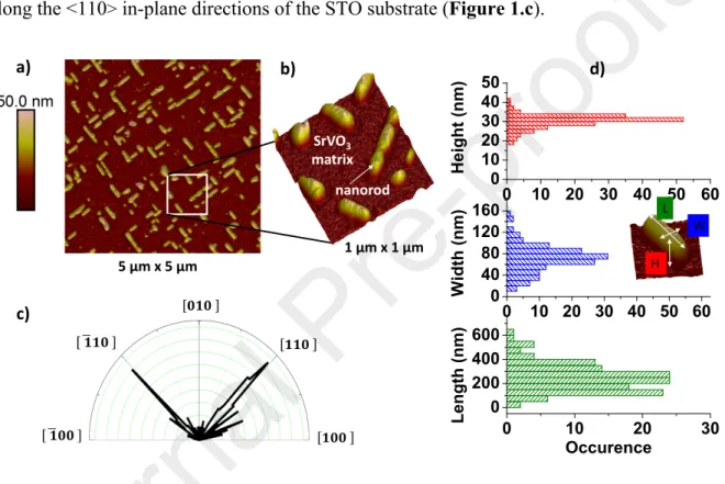
First, the topography of the obtained NRs is investigated with the AFM tapping mode. From the AFM topography of the surface of SVO thin films grown on STO, self-organized NRs are revealed in Figure 1. The scan area of 5 µm 5 µm (Figure 1.a) shows that the NRs form a two-dimensional network with specific orientations (Figure 1.b), the long axis being aligned along the <110> in-plane directions of the STO substrate (Figure 1.c).
SrVO3 matrix nanorod 1 µm x 1 µm 5 µm x 5 µm a) b) c) 0 200 400 600 0 10 20 30 H ei g h t (n m ) W id th ( n m ) L en g th ( n m ) Occurence 0 40 80 120 160 0 10 20 30 40 50 60 0 10 20 30 40 50 0 10 20 30 40 50 60 L W H d)
Figure 1. AFM tapping-mode topography image in ambient conditions for scan sizes: a) 5 µm × 5 µm and b) 1 µm × 1 µm. c) Distribution of the orientation of the NRs with respect to the [100] direction of the SVO film. d) Height, width and length distribution of the NRs measured from a).
.
The dimensions of the NRs were analyzed for an ensemble of 150 NRs. The height distribution (Figure 1.d) shows a narrow distribution with a mean value at 30 ± 4 nm. This value is slightly larger than the one found in previous studies,8,9 this change being attributed to
a longer annealing time. Thus, the growth of the NRs is not a self-limited mechanism, and NRs of different heights and sizes can be synthesized by adapting the growth and annealing
(width) and a long one (length). While the width distribution shows a rather narrow distribution around 80 nm, the long axis shows a broader distribution (Figure 1.d), ranging from 50 to 600 nm.
X-ray diffraction (XRD) pattern of the SVO studied film, grown on (100)STO, is represented in Figure SI-1. In addition to the (h00) peaks of the substrate, the pattern displays also the (h00) peaks of the SVO film, but the NRs reflections intensities are too weak to be observed. Therefore, electron diffraction was performed along the normal direction to the film surface. Electron diffraction pattern (EDP) along the [100] SVO zone axis displays weak reflections in addition to those of SVO (inset Figure 2.a). From these analyses, the Sr3V2O8
phase of the self-organized epitaxial NRs is identified. These reflections were ascribed to the (110) and (1-15) planes of the Sr3V2O8 phase along the [-552] zone axis (Figure 2.b). Actually,
the (110)Sr3V2O8 reflections (2d110 = 5.62 Å) are in coincidence with the (011)SVO reflection
(2d011 = 5.52 Å), due to the epitaxy between both materials. Since (011)SVO is equivalent to
(01-1)SVO, there are therefore two equiprobable possibilities for Sr3V2O8 to grow on SVO, i.e.
(110)Sr3V2O8 // (011)SVO and (110)Sr3V2O8 // (01-1)SVO. The two corresponding EDPs schemas are
shown in Figures 2.c and d, and the complete EDP simulation with the reflections of both variants together with the SVO reflections in Figure 2.b, well reproducing the experimental pattern.
Figure 2. a) EDP of the SVO film along the [100] zone axis. The inset shows weak reflections due to the NRs close to the strong reflections of SVO. b) Scheme of the experimental pattern showing the contributions of SVO (black circles) and of both NR variants (red and blue circles, respectively) along the [-552] zone axis of Sr3V2O8. The
(110)Sr3V2O8 reflections are in coincidence with the (011)SVO and (01-1)SVO
reflections. c) Scheme of the EDP of a single NR variant with the (110)Sr3V2O8 //
(011)SVO orientation. d) Same for the second variant with the (110)Sr3V2O8 // (01-1)SVO
orientation.
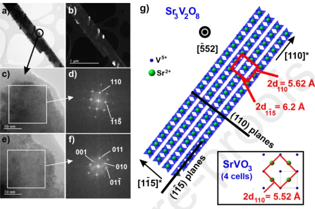
Figure 3.a and b show the TEM observations in bright field and dark field mode in plane-view of a fragment of the SVO film, obtained by collecting the sample surface with the help of a diamond scribe. To establish the direction of elongation, HRTEM was performed on a single NR (Figure 3.c). The fast Fourier transform (FFT) performed on the HRTEM image (Figure 3.d) corresponds to the [-552] zone axis of Sr3V2O8, with the [110]* direction parallel
to the NR elongation direction (as seen on Figure 2c). Moreover, for purpose of comparison, HRTEM and corresponding FFT were also registered on the SVO film next to the NR, and
confirms the previously established (110)Sr3V2O8 // (011)SVO relation (Figure 3.e,f). From these
observations, a sketch of the crystalline NR was established and drawn in Figure-3.g.
Figure 3. a),b) Bright field and dark field TEM images showing a plane-view of a fraction of the SVO film with several elongated NRs. c) HRTEM image of the NR encircled in a). d) FFT of the area surrounded in c), showing that the [110]* direction is parallel to the NR elongation. e) HRTEM image of an area of the SVO film close to the NR. f) FFT of the area surrounded in e), showing the orientation relationship between the NR and the SVO film. g) Scheme of the structure and of the in-plane orientation of a single NR along the [-552] zone axis. The long axis is parallel to the [110]* direction, while the short axis is parallel to the [1-15]* direction. The cell drawn in red is aligned on the cubic cell of the SVO film displayed in the inset. The epitaxial relationship is governed by the close mismatch between d110 of Sr3V2O8 and d110 of SVO.
The lattice spacing d110 of the cell of the NRs shows a low mismatch of 3.4 % with the
strained SVO matrix along the <110> directions, while along the perpendicular [-11-5] direction of the NRs, the mismatch is up to 14 %. Therefore, the growth of the NRs along their [110] directions is favored, leading to their elongated shape. The growth of the long axis of the NRs being therefore promoted compared to the short axis, the long axis shows a much broader distribution, yielding an aspect ratio distribution between 2 and 8.
In order to confirm the chemical and structural properties of the NRs, we have performed electron energy loss spectroscopy (EELS) and energy-filtering transmission electron microscopy (TEM) spectrum imaging (EFTEM-SI) with the help of an energy spectrometer combined to a TEM. In the TEM, electrons pass through the sample and lose a certain amount of their energy by inelastic interactions with the present elements. Therefore, EELS allows to discriminate the oxidation states of the V ions10. The EFTEM-SI technique allows to map the
spatial distribution of the oxidation states with the help of an energy filter and a CCD camera combined with the spectrometer11. Figure 4.a is a bright field zero-loss TEM micrograph
showing a plane-view of a fragment of the SVO film. The fragment of the SVO film is a 400 nm wide strip on which several elongated NRs are visible on its edge. EELS was performed on pure SVO, and on pure Sr3V2O8 areas (Figure 4.e). The EELS spectrum of SVO is similar to
that of previous works,12 while that of Sr
3V2O8 is similar to spectra of other V5+ vanadate phases,
such as LaVO412 and V2O5.13 EFTEM multiple linear least-squares (MLLS) fits of each valence
state (Figure 4.b.c) together with the combined RGB image (Figure 4.d) show that V5+ valence
state is present principally in the elongated NRs while V4+ is present in the matrix only. Indeed,
SVO films with a vanadium oxidation state V4+ are only stabilized at low oxygen pressure (10-4
-10-5 Pa) during deposition8. If the partial oxygen pressure is left after deposition at high
temperature, a higher and more stable vanadium oxidation state (V5+) can be induced at the
surface of the film, which crystallizes in a new Sr-V oxide parasitic phase with a higher valence state.
510
520
530
540
550
C
o
u
n
ts
(
a.
u
.)
Energy loss (eV)
VL3 VL2 OK Sr3V2O8NR SrVO3filma)
d)
b)
c)
2 1 2 1e)
Figure 4. a) Bright field zero-loss TEM image showing a plane-view of a fraction of the SVO film with several elongated crystals. b) V4+ state MLLS fit map of the same area.
c) V5+ state MLLS fit map. d) Combined RGB map. e) Vanadium-L
3,2 and oxygen-K
EELS spectra acquired at two locations: “1” corresponds to the SVO film and “2” to one Sr3V2O8 nanostructure.
SSRM imaging and tomography on the Sr3V2O8 nanorods
While SVO is a metallic paramagnetic material that can be used as electrode,14–17the
different stoichiometry of the NRs might lead to a significant change of the material resistivity. In the bulk form, Sr3V2O8, is an insulating material with low dielectric losses.18,19In order to
determine the local electrical properties of the self-organized Sr3V2O8 NRs, SSRM
measurements were performed. Based on an AFM, in SSRM measurements, a bias voltage (Vdc)
is applied to the sample while the scanning probe is grounded. In this local electrical mode, simultaneous mappings of the topography and local resistance are obtained. The current flows from the tip through the sample to the back-contact and is recorded through a seven decades logarithmic current amplifier with a current range (I) from 10 pA up to 0.1 mA.20–22 The SSRM
output voltage (Vout) corresponds to a logarithmic scale of the local resistance (R) of the
,
(1)V
out=± K × log
(
I × 10 6 Vdc)
=± K × log
(
106 R)
where ± is the sign of the applied DC bias voltage to the sample (Vdc), K = 1 V is the scale
factor of the amplifier, R the local resistance in Ohm and Vout is the output signal of the
logarithmic current amplifier of the microscope in Volt (see supplementary information figure SI-2 for more details)23–25.
For each pixel, the overall measured resistance (R) includes: the resistance of the probe, the spreading resistance, the resistance of the sample and the resistance of the back contact with the chuck.26 In order to determine the mechanisms describing the carrier transport properties of
the NRs, two Vdc biases with opposite polarities are applied. The measured mapping of the
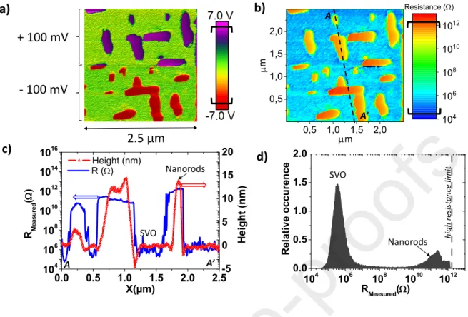
output signal Vout is represented in Figure 5Figure 5.a for two different bias voltages:
Vdc = + 100 mV for the upper part of the image and Vdc = -100 mV for the lower part (each
pixel of the scanned area is related to the corresponding color). For this acquisition a force of 4 µN is applied to the AFM cantilever (the applied force is calculated from the spring constant) The measured conductivity of the sample (SVO matrix and nanostructures) shows symmetric responses as a function of the sign of the applied Vdc bias, indicating that the contact between
the AFM conductive tip and the sample is ohmic-like in the range of here applied Vdc. The
resistance mapping, determined with the formula (1), is shown in Figure 5.b.
As we can see, all Sr3V2O8 NRs have a larger resistance than the SVO matrix. In Figure 5.c,
the profile of the local resistance and the topography along the line AA’ extracted from the Figure 5.b is displayed. In Figure 5.d, the histogram of the resistance, shows two markedly different resistance ranges for the SVO matrix (105 – 107 and the NRs (1010 to 1.4 ×
1012 On average, the NRs increase the total resistance through the sample by about 5 orders
104 106 108 1010 1012 0.0 0.5 1.0 1.5 2.0 R el at iv e o cc u re n ce RMeasured() 0,5 1,0 1,5 2,0 0,5 1,0 1,5 2,0 m m 104 106 108 1010 1012 Resistance () 0.0 0.5 1.0 1.5 2.0 2.5 104 106 108 1010 1012 1014 1016 -5 0 5 10 15 20 R () RM ea su re d ( ) X(µm) Height (nm) H ei g h t (n m ) A’ SVO Nanorods d) SVO Nanorods A c) b) A A’ hi gh re si st an ce lim it a) 2.5 µm + 100 mV - 100 mV
Figure 5. a) 2D-map of the Vout signal from SSRM mode. b) 2D-map of the local resistance.
c) Resistance profile along the line AA’. d) Resistance distribution in the scanned area. The brackets in the data scale indicate data threshold.
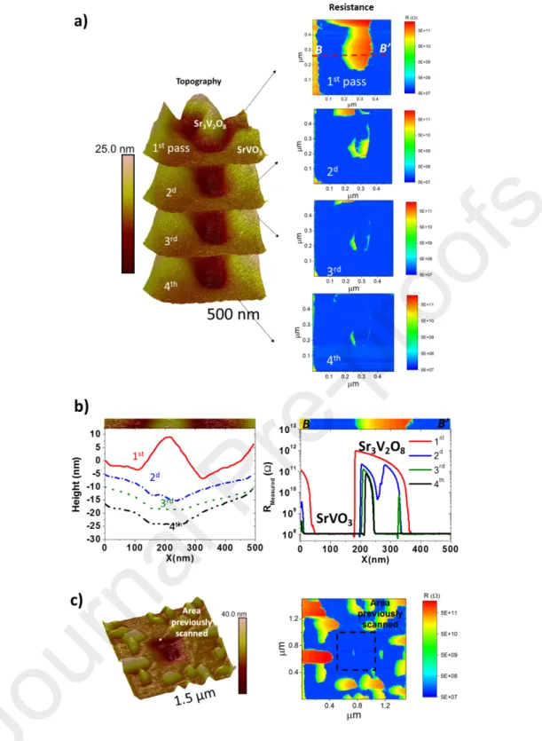
The particular mechanical property of the SSRM tip, which is diamond-coated, allows for unveiling the electrical properties in the depth of an individual NR by performing a resistance tomography, referred to as 3D-SSRM.17–20 The methodology of electrical AFM
tomography for 3D analysis is described in.30 Based on the tip-induced material removal and
subsequent scans, 3D-SSRM achieves electrical analysis of NRs in the third direction.22 The
topography and electrical resistance are simultaneously recorded on an individual NR (Figure 6), the scan area is 500 nm 500 nm. With four subsequent scans of the same area, the sample surface is progressively etched by the tip. As we can see, on Figure 6, due to the hard probe, matter is removed. During SSRM scan the probe indents and scratches the surface. After 4 scans, the tip digs the surface of the NR for a total depth of 55 nm (from 30 nm (pristine NR) to -25 nm). When the probe indents two times, the resulting topography recorded during the
indicates that a high resistance is still measured. Thereby 3d-SSRM investigations points out that the NRs is embedded within the SVO perovskite volume. In addition, a fifth SSRM scan of a larger area about 1.5 µm 1.5 µm is represented in Figure 6.c with corresponding topography and resistance mappings. The larger SSRM acquisition shows that the etched nanostructure at the center of the image leaves a 30 nm-deep hole behind. Figure SI-3-4 shows data obtained in another location of the studied film. This result is in agreement with the dissolution of the NRs by water that left holes inside the SVO matrix as observed earlier.9 Also,
this embedding can be observed in the EELS combined map (Figure 4.d), where the presence of V5+ ions is observed also inside the V4+ area only below the NRs.
The NRs show a higher level of resistance over the entire thickness of the nanostructure, in comparison with the SVO matrix, consistent with a different chemical composition. Furthermore, we note a change of the maximum resistance between the first scan and the next ones, which could be caused by the presence of species at the surface, may be carbonated species and other organic contaminants, making it more resistive.9,29 In addition, in Figure 6.a,
a small topographical depression is observed between the SVO matrix and the NR. This depression, observed on all the NRs, points toward a growth from the material available underneath a nucleation center in the SVO matrix and a change of the composition of the film in these areas, leading to the enhanced resistance.
Figure 6. 3D-SSRM results (500 nm × 500 nm) for successive scans: a) AFM topography acquisitions and resistance maps for each scan. b) Line profiles of the topography and resistance along the line BB’. c) Topography and SSRM 2D-map of a larger scan 1.5 µm x 1.5 µm centered on the area previously scanned.
Electrical properties of individual Sr3V2O8 nanorods
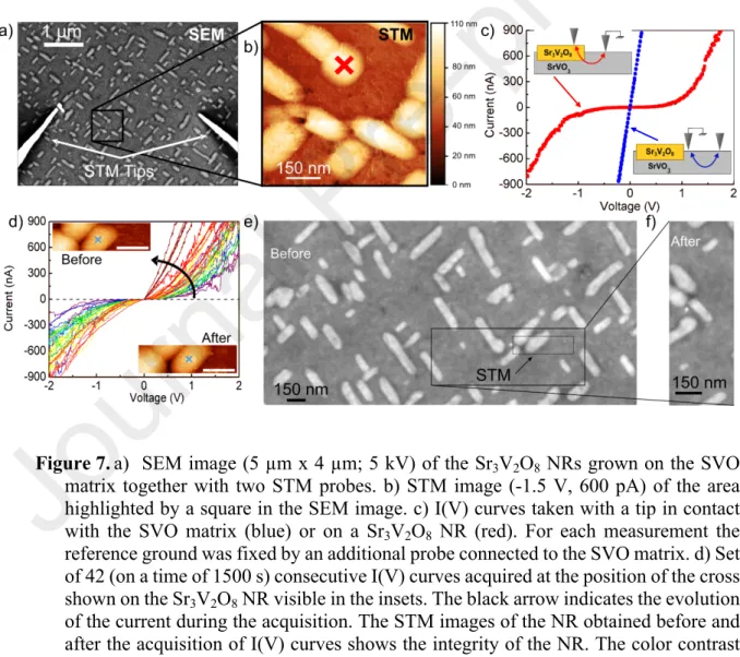
As water bridges between the AFM tip and the surface of the sample can play an important role in mechanical contacts, where they can affect friction in ambient conditions, for a comprehensive study, electrical measurements were also performed in UHV. A multiple-probe STM is used to selectively study the nanostructures and the matrix. In order to obtain reproducible contact resistances between the samples and the STM tips, the sample was degassed at 700°C, an annealing step that has been shown to remove the strontium carbonates species.7 The similarity between the SEM image of the sample acquired after the high
temperature annealing (Figure 7.a) and the AFM image (Figure 1.a) reveals that the Sr3V2O8
NRs do not undergo major modifications during this post-treatment in UHV. The stability of the NRs is further confirmed by the STM scan performed on a 1 µm x 1 µm area (Figure 7.b) where the NRs are clearly distinguished. Here the STM is used as a nanometer-precision tool for geometrical measurement and contact positioning of the tips. Keeping one STM tip in contact with the SVO matrix, a second STM tip selectively contacts the SVO matrix or individual NR to drive a current through the structure. The transport properties of individual nanostructures and the matrix are compared in Figure 7.c. The I(V) measurements performed on the SVO matrix (blue) shows a metallic behaviour, yielding a resistance of 2.2x10⁵ Ω
consistent with the typical resistances determined with SSRM mode. In contrast, the I(V) curve acquired on the NR exhibits a non-linear characteristic. In the linear region around zero volt, a resistance of 1.5x10¹¹ Ω is found, in good agreement with the SSRM profile (performed at low
biases) of Figure 6.c. As the annealing process is known to lead to the removal of the carbonated species and other organic contaminants that could modify the resistance at the surface of the NRs, this result confirms the high resistance of the bulk part of the NRs and stresses on their robustness since their structural and physical properties (shape, size, and transport) are maintained despite their annealing up to 700°C in UHV.
As the STM tips are known to drift in time, we acquired consecutive I(V) spectra over 25 minutes. As shown in Figure 7.d, which displays 42 consecutive voltage sweeps, the current increases by about two orders of magnitude at a fixed voltage. While this increase can be caused by a larger contact area between the tip and the NR or/and by the strain of the lattice that is known to change the electrical conductivity of correlated transition-metal oxides,31 it is
interesting to observe that these effects do not modify the morphology of the NR. As shown by the insets of Figure 7.d, obtained before and after the acquisition of the spectra, the UHV environment preserves the integrity of the NRs, suggesting that the water meniscus contributes to the efficient etching of the NR in SSRM measurement performed in air.
Figure 7. a) SEM image (5 µm x 4 µm; 5 kV) of the Sr3V2O8 NRs grown on the SVO
matrix together with two STM probes. b) STM image (-1.5 V, 600 pA) of the area highlighted by a square in the SEM image. c) I(V) curves taken with a tip in contact with the SVO matrix (blue) or on a Sr3V2O8 NR (red). For each measurement the
reference ground was fixed by an additional probe connected to the SVO matrix. d) Set of 42 (on a time of 1500 s) consecutive I(V) curves acquired at the position of the cross shown on the Sr3V2O8 NR visible in the insets. The black arrow indicates the evolution
of the current during the acquisition. The STM images of the NR obtained before and after the acquisition of I(V) curves shows the integrity of the NR. The color contrast corresponds to the one displayed in b). The scale bar is 150 nm. e) SEM image of NRs grown on the SVO matrix that was acquired prior to the acquisition of the I(V) curves and where the area imaged in d) is highlighted by the dotted rectangle. f) SEM image
of a more limited area (with rotation of 90°) that shows the morphological inalterability of the NR after the acquisition of the I(V) curves.
CONCLUSION
Structural and electrical properties of self-organized Sr3V2O8 NRs formed on SVO thin
films were investigated by TEM, EELS, EFTEM and local electrical probe SSRM and STM techniques. The epitaxial relationship between the NRs and the SVO matrix was deduced and EELS and EFTEM-SI underline the vanadium oxidation state (V5+) of the Sr
3V2O8 NRs.While
the SVO matrix is metallic, SSRM and STM measurements revealed the insulating character of the self-organized NRs. Moreover, we analysed the local resistivity of the Sr3V2O8 NRs in full
three-dimensions. This 3D-analysis shows that the NRs are embedded in the SVO perovskite matrix. As a result, the Sr-rich composition of the NRs does not only account for the higher electrical resistance of the NRs, but also for its faster mechanical etching rate due to the higher reaction of the NRs surface with water in comparison with the SVO matrix. These results open the way for the preparation of local imprints on a metallic surface and deposition of nano-objects for accurate electrical characterizations of individual object as demonstrated in this paper.
METHODS
Synthesis of Sr3V2O8 nanorods
We used the pulsed laser deposition technique with a KrF excimer laser ( = 248 nm) with an energy density of 1.85 J/cm² and 2 Hz repetition rate. Thin films were grown on single-crystal (SurfaceNet GmbH) (100)STO substrates (10 × 10 × 0.5 mm3) placed at 5 cm opposite
of a ceramic SrVO3 target. The deposition temperature was 760°C with partial oxygen pressure
fixed at 10-4 Pa. Film thickness of approximately 100 nm have been determined by conventional
step-meter measurements (Bruker Dektak 8). The nanostructures are obtained after growth when the O2 deposition atmosphere is maintained during the cooling. It is important to note that
if the temperature is decreased just after deposition and the oxygen partial pressure is removed, a smooth SVO surface is obtained. Consequently, the size of nanostructures can be tuned by controlling the partial oxygen pressure and exposition time at high temperature before the cooling. In previous works, we have analyzed the crystallographic structure of the SVO film8,32,
showing that it is epitaxially grown on the STO substrate with a cube-on-cube relationship. X-ray diffraction (XRD) characterization of thin films was carried out using a θ–2θ Bragg-Brentano diffractometer (Bruker AXS D8 Advanced) working with a monochromatized Cu Kα1 radiation and equipped with a 1D detector (192 channels).
Electron Energy Loss Spectroscopy (EELS) and Energy Filtered Transmission Microscopy Scanning Imaging (EFTEM-SI) were performed by using a Gatan Imaging Filter (GIF) Quantum ER spectrometer coupled to a transmission electron microscope (TEM) 2100 Jeol instrument. The sample was prepared by scratching its surface with a diamond scribe. Small fragments of the sample containing film and nanostructures were then collected on a
commercial TEM carbon-coated copper microgrid. EELS spectra were collected at 120 kV, with an energy resolution of 0.75 eV, at a camera length L = 6 cm, and were corrected of plural inelastic scattering contribution after background subtraction. EFTEM-SI images were recorded at 200 kV, with an energy step of 1 eV and an energy slit width of 1 eV. The obtained data cube was corrected from X-ray artefacts and spatial drift. Reference spectra for the pure V4+ and V5+ states were extracted from the raw data, in spatial areas corresponding to the matrix
and the nanostructures, respectively. Using these reference spectra, multiple linear least-squares (MLLS) fitting was then performed to extract chemical shift maps of V4+ (SrVO
3 phase) and
V5+ state (Sr
3V2O8 phase), by using the Gatan Digital Micrograph software.
Schemes of structures and of electron diffraction patterns were drawn with the commercial CrystalMaker software.
Near field experiments are carried out with a Bruker AFM. Acquisitions of topology and local electrical properties are obtained under ambient conditions. A vibration isolation table is employed to eliminate ground vibration and acoustic noise. In order to well-define the morphology of the nanostructured surface, the AFM tapping-mode33 is used with a resolution
of 512 × 512 pixels. In this topography mode, a silicon tip with a nominal tip radius of < 10 nm is employed.
The SSRM mode used for probing the local electrical properties. Based on an AFM, SSRM is a nano-electrical contact mode. During measurement, a conductive antimony (n)-doped silicon probe, with a coated boron (p)-doped diamond film, is in strong contact with the analyzed surface of the sample. The spring constant of the probe is 42 N/m. In our case, it must be noted that a relatively high pressure about 4 µN is applied on the tip and that after each scan, the tip integrity was verified by using a calibration grid composed of an array of sharp tips (TGT1-NT-MDT). In this nano-electrical mode, the current flowing from the conductive tip
resistance (the conductive tip resistance, the spreading resistance of the semiconductor under the contact, the bulk resistance of the sample and the back-contact resistance) is experimentally determined29 by a logarithmic current amplifier.
Scanning tunnelling microscopy (STM) and multiple probe nano-transport measurements were done in ultra-high vacuum (UHV, base pressure lower than 5x10⁻¹⁰ mbar)
under scanning electron microscope (SEM) monitoring. The system is operated with a unique control system able to run the four STM tips independently with sub-nanometer precision.34
Tungsten tips were prepared by an electrochemical etching in NaOH and thoroughly cleaned in UHV. The electrical measurements were performed in UHV, always with the electron beam turned off.
AUTHOR INFORMATION Corresponding Author
Rosine COQ GERMANICUS *rosine.germanicus@unicaen.fr Arnaud FOUCHET *arnaud.fouchet@ensicaen.fr
ACKNOWLEDGMENT
The authors thank the French Agence Nationale de la Recherche (ANR) in the framework of the POLYNASH project (ANR-17-CE08-0012), the Réseaux d’Intérêts Normands RIN PLACENANO, the EQUIPEX program Excelsior (Grant No. ANR-11-EQPX-0015), the H2020 program (Grant No. PITN-GA-2016-722176, Indeed Project), the RENATECH network and the Labex CHARMMMAT (ANR-11-LABEX-0039) from IDEX Paris-Saclay, the Région Bretagne, Rennes Métropole, the Département d’Ille et Vilaine and the European Union (CPER-FEDER 2007–2014, Présage Nos. 39126 and 37339, and CPER 2015-2020 MULTIMAT ScanMAT) for their financial support. The authors are also thankful for the collaboration with Digital Surf through Mount Shasta program.
REFERENCES
(1) Wang, X.; Zhuang, J.; Peng, Q.; Li, Y. A General Strategy for Nanocrystal Synthesis. Nature 2005, 437 (7055), 121–124.
(2) Biswas, A.; Bayer, I. S.; Biris, A. S.; Wang, T.; Dervishi, E.; Faupel, F. Advances in Top–down and Bottom–up Surface Nanofabrication: Techniques, Applications & Future Prospects. Advances in Colloid and Interface Science 2012, 170 (1), 2–27. (3) Chen, Y.; Pépin, A. Nanofabrication: Conventional and Nonconventional Methods.
ELECTROPHORESIS 2001, 22 (2), 187–207.
(4) Lasers and Moore’s Law: SPIE Professional magazine
https://spie.org/membership/spie-professional-magazine/archives/octob-2010-spie-professional/lasers-and-moores-law?
(5) Zubko, P.; Gariglio, S.; Gabay, M.; Ghosez, P.; Triscone, J.-M. Interface Physics in Complex Oxide Heterostructures. Annual Review of Condensed Matter Physics 2011, 2 (1), 141–165.
(6) Zabaleta, J.; Valencia, S.; Kronast, F.; Moreno, C.; Abellán, P.; Gázquez, J.; Sepehri-Amin, H.; Sandiumenge, F.; Puig, T.; Mestres, N.; et al. Photoemission Electron Microscopy Study of Sub-200 Nm Self-Assembled La 0.7 Sr 0.3 MnO 3 Epitaxial Islands. Nanoscale 2013, 5 (7), 2990–2998.
(7) Szafraniak, I.; Harnagea, C.; Scholz, R.; Bhattacharyya, S.; Hesse, D.; Alexe, M. Ferroelectric Epitaxial Nanocrystals Obtained by a Self-Patterning Method. Appl. Phys. Lett. 2003, 83 (11), 2211–2213.
(8) Bérini, B.; Demange, V.; Bouttemy, M.; Popova, E.; Keller, N.; Dumont, Y.; Fouchet, A. Control of High Quality SrVO3 Electrode in Oxidizing Atmosphere. Adv. Mater. Interfaces 2016, 3 (18).
(9) Bourlier, Y.; Frégnaux, M.; Bérini, B.; Fouchet, A.; Dumont, Y.; Aureau, D. Surface Characterizations and Selective Etching of Sr-Rich Segregation on Top of SrVO3 Thin-Films Grown by Pulsed Laser Deposition. ChemNanoMat 2019, 5 (5), 674–681.
(10) Egerton, R. F. Electron Energy-Loss Spectroscopy in the TEM. Rep. Prog. Phys. 2008, 72 (1), 016502.
(11) Lavergne, J.-L.; Martin, J.-M.; Belin, M. Interactive Electron Energy-Loss Elemental Mapping by the “Imaging-Spectrum” Method. Microsc. Microanal. Microstruct. 1992, 3 (6), 517–528.
(12) Fitting Kourkoutis, L.; Hotta, Y.; Susaki, T.; Hwang, H. Y.; Muller, D. A. Nanometer Scale Electronic Reconstruction at the Interface between LaVO3 and LaVO4. Phys. Rev. Lett. 2006, 97 (25), 256803.
(13) Laffont, L.; Wu, M. Y.; Chevallier, F.; Poizot, P.; Morcrette, M.; Tarascon, J. M. High Resolution EELS of Cu–V Oxides: Application to Batteries Materials. Micron 2006, 37 (5), 459–464.
(14) Moyer, J. A.; Eaton, C.; Engel-Herbert, R. Highly Conductive SrVO 3$ as a Bottom
Electrode for Functional Perovskite Oxides. Advanced Materials 2013, 25 (26), 3578– 3582.
(15) Zhang, L.; Zhou, Y.; Guo, L.; Zhao, W.; Barnes, A.; Zhang, H.-T.; Eaton, C.; Zheng, Y.; Brahlek, M.; Haneef, H. F.; et al. Correlated Metals as Transparent Conductors. Nature Materials 2015, 15 (2), 204–210.
(16) Backes, S.; Rödel, T. C.; Fortuna, F.; Frantzeskakis, E.; Le Fèvre, P.; Bertran, F.; Kobayashi, M.; Yukawa, R.; Mitsuhashi, T.; Kitamura, M.; et al. Hubbard Band versus Oxygen Vacancy States in the Correlated Electron Metal SrVO 3. Physical Review B 2016, 94 (24), 241110.
(17) Fouchet, A.; Rault, J. E.; Allain, M.; Bérini, B.; Rueff, J.-P.; Dumont, Y.; Keller, N. Interface Chemical and Electronic Properties of LaAlO3/SrVO3 Heterostructures. Journal of Applied Physics 2018, 123 (5), 055302.
(18) Khatri, P.; Behera, B.; Choudhary, R. N. P. Structural and Electrical Properties of Sr3V2O8 Ceramics. phys. stat. sol. (b) 2009, 246 (5), 1118–1123.
(19) Pati, B.; Choudhary, R. N. P.; Das, P. R. Phase Transition and Electrical Properties of Strontium Orthovanadate. Journal of Alloys and Compounds 2013, 579 (Supplement C), 218–226.
(20) Eyben, P.; Denis, S.; Clarysse, T.; Vandervorst, W. Progress towards a Physical Contact Model for Scanning Spreading Resistance Microscopy. Materials Science and Engineering: B 2003, 102 (1), 132–137.
(21) Li, H.; Jiang, C.; Metzger, W. K.; Shih, C.; Al-Jassim, M. Microscopic Real-Space Resistance Mapping Across CdTe Solar Cell Junctions by Scanning Spreading Resistance Microscopy. IEEE Journal of Photovoltaics 2015, 5 (1), 395–400.
(22) Vandervorst, W.; Fleischmann, C.; Bogdanowicz, J.; Franquet, A.; Celano, U.; Paredis, K.; Budrevich, A. Dopant, Composition and Carrier Profiling for 3D Structures.
Materials Science in Semiconductor Processing 2017, 62 (Supplement C), 31–48. (23) Avila, A.; Bhushan, B. Electrical Measurement Techniques in Atomic Force
Microscopy. Critical Reviews in Solid State and Materials Sciences 2010, 35 (1), 38– 51.
(24) Stetson, C.; Yoon, T.; Coyle, J.; Nemeth, W.; Young, M.; Norman, A.; Pylypenko, S.; Ban, C.; Jiang, C.-S.; Al-Jassim, M.; et al. Three-Dimensional Electronic Resistivity Mapping of Solid Electrolyte Interphase on Si Anode Materials. Nano Energy 2019, 55, 477–485.
(25) Meuris, M. A. J.; Vandervorst, W. B. M.; Wolf, P. de. Method for Determining the Resistance and Carrier Profile of a Semiconductor Element Using a Scanning Proximity Microscope. US5585734A, December 17, 1996.
(26) De Wolf, P.; Geva, M.; Hantschel, T.; Vandervorst, W.; Bylsma, R. B.
Two-Dimensional Carrier Profiling of InP Structures Using Scanning Spreading Resistance Microscopy. Appl. Phys. Lett. 1998, 73 (15), 2155–2157.
(27) Xu, M. W.; Hantschel, T.; Vandervorst, W. Three-Dimensional Carrier Profiling of InP-Based Devices Using Scanning Spreading Resistance Microscopy. Appl. Phys. Lett. 2002, 81 (1), 177–179.
(28) Mody, J.; Zschatzsch, G.; Kolling, S.; De Keersgieter, A.; Eneman, G.; Kambham, A.; Drijbooms, C.; Schulze, A.; Chiarella, T.; Horiguchi, N. 3D-Carrier Profiling in FinFETs Using Scanning Spreading Resistance Microscopy; 2011.
(29) Coq Germanicus, R.; Leclère, Ph.; Guhel, Y.; Boudart, B.; Touboul, A. D.; Descamps, P.; Hug, E.; Eyben, P. On the Effects of a Pressure Induced Amorphous Silicon Layer on Consecutive Spreading Resistance Microscopy Scans of Doped Silicon. Journal of Applied Physics 2015, 117 (24), 244306.
(30) Celano, U.; Goux, L.; Belmonte, A.; Schulze, A.; Opsomer, K.; Detavernier, C.; Richard, O.; Bender, H.; Jurczak, M.; Vandervorst, W. Conductive-AFM Tomography for 3D Filament Observation in Resistive Switching Devices. In 2013 IEEE
International Electron Devices Meeting; 2013; pp 21.6.1-21.6.4.
(31) Cao, J.; Ertekin, E.; Srinivasan, V.; Fan, W.; Huang, S.; Zheng, H.; Yim, J. W. L.; Khanal, D. R.; Ogletree, D. F.; Grossman, J. C.; et al. Strain Engineering and One-Dimensional Organization of Metal–Insulator Domains in Single-Crystal Vanadium Dioxide Beams. Nature Nanotechnology 2009, 4 (11), 732–737.
(32) Fouchet, A.; Allain, M.; Bérini, B.; Popova, E.; Janolin, P.-E.; Guiblin, N.; Chikoidze, E.; Scola, J.; Hrabovsky, D.; Dumont, Y.; et al. Study of the Electronic Phase
Transition with Low Dimensionality in SrVO3 Thin Films. Materials Science and Engineering: B 2016, 212, 7–13.
(33) Coq Germanicus, R.; Picard, E.; Domenges, B.; Danilo, K.; Rogel, R. Microstructure and Electrical Characterization Based on AFM of Very High-Doped Polysilicon Grains. Applied Surface Science 2007, 253 (14), 6006–6012.
(34) Berthe, M.; Durand, C.; Xu, T.; Nys, J. P.; Caroff, P.; Grandidier, B. Combined STM and Four-Probe Resistivity Measurements on Single Semiconductor Nanowires. In Atomic Scale Interconnection Machines; Joachim, C., Ed.; Advances in Atom and Single Molecule Machines; Springer Berlin Heidelberg, 2012; pp 107–118.
Highlights :
Self organized epitaxial Sr3V2O8 nanorods on SrVO3 metallic matrix
Specific local electric properties by conductive Atomic Force Microscopy and scanning tunneling microscopy
Three dimensional resistance mapping of the nanorods by 3D-Spreading Resistance Microscopy mode
Rosine Coq-Germanicus, Arnaud Fouchet: Conceptualization, Methodology, Software, Data curation, Writing- Original draft preparation, Supervision.
Bruno Bérini, Yves Dumont, Yoan Bourlier, Valérie Demange, Vincent Notot, Maxime Berthe, Alexis Boileau, Matthieu Euchin, Damien Aureau, Mathieu Fregnaux, Bruno Grandidier, Adrian David, Wilfrid Prellier, Louis Biadala: resources, investigations, Visualization
Declaration of interests
☒The authors declare that they have no known competing financial interests or personal relationships that could have appeared to influence the work reported in this paper.
☐The authors declare the following financial interests/personal relationships which may be considered as potential competing interests:
![Figure 2. a) EDP of the SVO film along the [100] zone axis. The inset shows weak reflections due to the NRs close to the strong reflections of SVO](https://thumb-eu.123doks.com/thumbv2/123doknet/14402819.510293/7.892.176.770.95.642/figure-edp-inset-shows-reflections-close-strong-reflections.webp)