Computer-Aided Design and Optimization of
dc/de Power Converters
by
Timothy Carl Neugebauer
B.S., Union College (1997)
Submitted to the Department of Electrical Engineering and Computer Science
in Partial Fulfillment of the Requirements for the Degree of
Master of Science in Electrical Engineering and Computer Science
at the Massachusetts Institute of Technology
September, 1999
@ 1999, Massachusetts Institute of Technology. All rights reserved.
Signature of Author
Certified by_
Dep t of Electrical E eering and Computer Science September, 1999
John G. Kassakian Professor of Electrical Engineering and Computer Science Thesis Supervisor
Certified by_
David J. Perreault Research Scientist Secondary Thesis Supervisor
Accepted by
MASSACHUSETTS INSTITUTE OF TECHNOLOGY
Arthur C. Smith Chairman, Department Committee on Graduate Theses
Computer-Aided Design and optimization of dc/dc Power Converters by
Timothy Carl Neugebauer
Submitted to the Department of Electrical Engineering and Computer Science In Partial Fulfillment of the Requirements for the Degree of
Master of Science in Electrical Engineering
Abstract
The imminent introduction of a dual-voltage automotive electrical system has motivated the development of dc/dc converters that are optimized it terms of price, weight, and volume. This thesis investigates the design and optimization of dc/dc converters for dual-voltage automotive electrical system. A prototype dc/dc converter is developed and experimental evaluated, and is used to identify a number of tradeoffs and critical design issues. Based on this information, a CAD optimization tool is developed which allows the design space to be rapidly explored and highly optimized converter design to be developed. The CAD optimization tool is also used to study the effects of variations in system-level specifications on the characteristics of optimized converters.
Thesis Supervisor: John G. Kassakian
Professor of Electrical engineering
Secondary Thesis Supervisor: David J. Perreault Research Scientist
Acknowledgments
This is the section in which I thank lots of people for all the help they have provided me, intellectually or otherwise, up to and including the time in which this thesis is complete.
All the characters and events portrayed on this page are fictional, and any resemblance to real people or incidence is purely coincidental.
I am most grateful to David Perreault and Harvey Callahan for all the technical help they have provided. I doubt there exists a question in EE that they could not solve and fully explain. I would also like to thank Ms. Dave for allowing her husband to help me for the past two years.
I would also like to thank the following people: To Mom, just because you're Mom.
To J.G.K., T.K., T.J., and G.D. for providing me with the opportunity that I had always dreamed about.
To V.M. and K.J. for all the work you've done. To Flo, I could never ask for a better friend.
To V.C. and L.N.P. for giving everyone in the lab something to laugh about. To the makers of Microsoft Office and other related software, for providing me with the unique pleasure of using your products, which was a once in a lifetime
experience.
To the makers of the Unix program LaTex, whose product I will be using for any other major documents that I will have to write.
To B.M., for your thesis was an enormous aid to my research.
To the various members of research unit number 1, for all the late night meeting that occurred.
To my brothers Brian and John, my father, mother, grandmother, and the rest of my family, for providing me with a place I could always go home to.
To the people of L.E.E.S. who also providing me with an office that was just as good as any home.
To the programmers of Blizzard, the makers of StarCraft and Diablo. To Hoss for bringing a little part of Texas into the lab.
To Scott Adams, for showing that engineers need a sense of humor.
To Fred, for he is like the twin brother I never had. He is also one of the top 3 xkobo players at MIT.
To J.G.G., T.B., and T.N.G. for your help in TimCAD's database. To all my friends at Union college, A.C., M.L., and E.H. to name a few. To everyone I forgot to list.
Table of Contents
Chapter 1 Introduction 13 1.1 A Dual-voltage Architecture 13 1.2 Thesis objectives 15 1.3 Thesis Organization 16 Chapter 2Design of the Prototype Converter 17
2.1 Requirements 17
2.1.1 Power Levels 17
2.1.2 EMI Limits 19
2.1.3 Ambient Temperature 20
2.2 Tradeoffs 21
2.2.1 Modular or Single Structure 21
2.2.2 Effects of Number of Cells on Output Ripple 23 2.2.3 Effects of the Number of Cells and Switch Type on
the Temperature Rise and Required Heatsink 26
2.2.4 Cells Inductance and Filter Size 28
2.3 The Prototype Converter 29
2.3.1 Major Components 29
2.4 Testing Results 33 2.4.1 Transient Tests 34 2.4.2 EMI Measurements 34 2.4.3 Thermal Measurements 37 2.5 Conclusions 37 Chapter 3 TimCAD Architecture 39 3.1 Optimization 39 3.2 Program Structure 42 3.2.1 User Interface 42 3.2.2 Control Loop 43 3.2.3 Design Algorithm 44 3.2.4 Device Models 46 3.2.5 The Database 46 3.3 Program Objects 48 3.3.1 CRecordset Objects 48 3.3.2 CDialog Objects 49
3.3.3 The CDocument Object 49
3.4 Program Operation 49
3.4.1 Installing TimCAD 49
3.4.2 Starting Up 47
3.5 Conclusions
Chapter 4
Results
4.1 Limitations of the Results
4.2 The Baseline System
4.3 A Design Comparison 4.4 Identifying Design Trends
4.5 The Effects of Power Rating
4.6 The Effects of Ambient Temperature
4.7 The Effects of EMI Limits
4.8 Conclusions
Chapter 5
Device Models and Heatsinks
5.1 Two MOSFETs as Switches
5.2 MOSFET and a Diode as Switches 5.3 Heat Sinking
5.4 Conclusions
Chapter 6
Passive Elements and Filters
6.1 The Converter Inductor
53 53 54 56 56 57 59 61 63 65 66 73 76 79 81 82 52
6.1.1 Overview 82
6.1.2 Initial Design Pass 85
6.1.3 Temperature Rise Limit 86
6.2 EMI Filter Inductor Design 88
6.2.1 Overview 88
6.2.2 Initial Design Pass 88
6.2.3 Temperature Rise Limit 91
6.3 Capacitors 92
6.4 Filters 93
6.4.1 Introduction 93
6.4.2 Filter Specifications and Measurements 94
6.4.3 Filter Design Overview 97
6.4.4 Filter Type 1 98
6.4.5 Filter Type 2 99
6.4.6 Filter Type 3 101
6.4.7 Summary of the Filter Design 102
6.5 Conclusions 103
Chapter 7
Conclusions 105
7.1 Thesis Conclusions 105
References Appendix A Appendix B Appendix C Appendix D Appendix E Voltage Limits Loadlist Schematics Functions Flowcharts 111 113 123 129 199 109
Chapter 1
Introduction
A revolution in the automotive electrical system is imminent. The electrical needs
of the automobile are ever increasing whereas the power available from conventional
alternators is reaching a saturation point. The members of the MI T./Industry Consortium on Advanced Automotive Electrical/Electronic Components and Systems have agreed that a dual-voltage system is the next evolutionary step for automotive electrical systems. High power loads would be moved up to a high-voltage bus, while incandescent lighting, electronics, and other loads that benefit from a lower voltage can remain on the
(currently-used) low-voltage bus. With the advent of the dual-voltage system, new high-voltage, high-power loads that were impractical to implement in the 14 V system will become available. Components and system benefits that will accrue due to the
dual-voltage system are described in [1-3].
1.1 A Dual-voltage Architecture
The dual-voltage system will require electrical energy to be supplied to two voltage busses. One widely considered method for doing this is illustrated in Fig. 1.1. A high voltage alternator supplies the high-voltage bus, while the low-voltage bus is
powered from the high-voltage bus via a dc/dc converter. The dc/dc converter can
provide a stable, well-controlled voltage on the lower bus. The amount of current flowing
from one bus to another can be easily controlled and limited with the converter. A
bi-directional converter can be employed in order for the low voltage bus to temporarily
power the high voltage bus so that the high-voltage battery can be recharged from the
low-voltage battery. These capabilities make the dc/dc converter-based system the most
desirable of available options from a performance standpoint.
The major drawback to the dc/dc converter-based architecture is the cost of the
converter. The converter is constructed from relatively high-cost components, such as
high-frequency power switches, capacitors, and magnetic elements. Large input and
output power filters are also needed to attenuate the conducted EMI generated by the
switching action of the power converter. Thus, the viability of the architecture depends
upon the ability to develop power converters at a low manufactured cost.
This thesis will address two main challenges in the design of the dc/dc converter.
The first challenge is to develop an automated method for finding an appropriate design
that will minimize the price, weight and volume of the dc/dc converter based on a set of
specifications. The second challenge is to develop a method for finding the sensitivity of
the price, weight and volume of an optimized converter to system-level parameters such
as the power rating, ambient temperature, or EMI limit.
Estimates' of the power requirements for luxury cars employing dual-voltage
electrical systems indicate an average 14 V loading of 600 - 800 W, with peak loads exceeding this by a factor of two or more. This suggests the need for a dc/dc converter
with an output power rating of 800 - 1000 W if a 14 V battery is used, and much higher
if a 14 V battery is not employed. As more loads are redesigned and moved to the 42 V
bus (leaving lighting and electrical loads on the 14 V bus), one might expect the
converter power requirements to be reduced to the 400 - 500 W range.
For the converter to be used in the automotive environment it must meet several
other requirements. If the dc/dc converter is to be placed under the hood it must be
designed to operate in a high ambient temperature. Furthermore, the converter will have
to meet extremely tight electromagnetic interference (EMI) requirements to prevent it
from interfering with other equipment on the vehicle. The converter will also need to be
configured to control the charging of the 14 V battery, and accept input from an external
energy management scheme that will direct the power flow to ensure that neither battery
becomes discharged.
A wide range of design possibilities exists for a dc/dc converter in the automotive application. The designer can choose among a wide range of subsystem topologies,
design parameters, and component types to design a converter. Because of this large
design space, and the tight interrelation among many of the design choices, identifying
the converter designs that best meet the design objective is extremely difficult in practice.
It is also difficult to ascertain a priori the effects of system level parameter variations on
the resulting price, weight, and volume of the "best" converter design.
1.2 Thesis Objectives
The dc/dc converter is not a new device, but introducing it as a component in the
automotive electrical system is a new application with unique requirements. Furthermore,
are unique to this new application. The first objective of this thesis is to develop and
evaluate a prototype dc/dc converter for this application.
The second objective of this thesis is to investigate the optimization of power
converters for this application. The design of a converter involves numerous tradeoffs
that make optimization extremely challenging. To meet this challenge, a computer-aided
design (CAD) optimization tool has been developed. The CAD program allows the
design space to be rapidly explored for optimal designs and design strategies.
The last objective of this thesis is to use this dc/dc converter optimization
program to examine trends within the design space. These trends will show the
sensitivities of the converter price, weight and volume to changes in system
specifications. The examination of these trends will inform the auto industry as to the
quantitative effects of several major system level choices.
1.3 Thesis Organization
This thesis contains seven chapters including this introductory chapter. Chapter 2
covers the design and evaluation of a prototype converter, describing the major tradeoffs
and choices. The optimization routine used to analyze the system is described in Chapter
3. Chapter 3 also contains information about the structure of the CAD program and directions for its use. Results from the program are shown in Chapter 4, including the
sensitivity of the converter characteristics to power rating, ambient temperature, and EMI
specifications. Chapters 5 and 6 contain the models for the devices, passive elements and
Chapter 2
Design of the Prototype Converter
In the course of this thesis a prototype dc/dc converter was designed and built.
The purpose of developing the prototype converter was to provide an understanding of
the converter design tradeoffs, and to allow operational experience to be gained with
power converters in this application. For purposes of this thesis, the prototype converter
is useful for validating component models in the optimization code. The converter has
been designed using many models (or early version of the models) used in the
computer-aided design optimization program, but without the benefits of automation of the process.
The prototype converter described here has also been used in a number of other
automotive electrical system projects both at M.I.T. and at the Ford Scientific Research
Laboratories in Dearborn, Michigan.
2.1 Requirements
2.1.1 Power Levels
The proposed dual-voltage electrical system for the next generation of automobiles will
contain a 42 V and a 14 V bus. The current automotive electrical system, as shown in Fig.
2.1a, consists of an alternator, a 12 V battery (regulated to 14 V for charging), and a
single 14 V bus. Many specific forms of the new dual-voltage system are possible, but
the general form of the new voltage system is illustrated in Fig. 2.1b. Of the candidate
a) b) C) alternator 12 V 14 V Loads new New alternator Electrical System to 1
provide both Lo4ds
14 and 42 42 V Lod
volts Loads
high voltage _L6 v
alternator 42 V
Loads
Figure 2.1: (a) The conventional automotive electrical system, (b) the proposed dual voltage automotive electrical system, and (c) an example of a dual voltage system implementation.
alternator and a dc/dc converter, as illustrated in Fig. 2.1 c.
The Forum Bordnetz, a European automotive discussion group, has proposed a set
of specifications for the new electrical system [4]. These specifications, which are
summarized in Appendix A, set the maximum and minimum voltages for both busses
under various conditions. The static voltage of the high voltage bus can vary from 33 to
52 V, and the static voltage of the lower voltage bus can vary from 12 to 16 V when the engine is running. These limits have been adopted for the design of the prototype
converter.
In order to determine the power level of the electrical system a comprehensive list
major loads will be moved to the higher bus, and that many other loads will initially
remain on the lower bus and be transferred to the higher bus at a later time. With this
assumption the load list was examined to determine the worst case and nominal power
requirements for the low-voltage bus. Based on the load list, the nominal power for the
low-voltage bus was predicted to be approximately 700 W, whereas the peak power
needed by the system would be approximately 1500 W. In order for the low-voltage
system to operate with these power demands, either the dc/dc converter would have to be
sized to deliver the peak power required, or a 12 V battery is needed in the system. To
supply 700 W to the 14 V bus the converter would need to deliver between 43.8 and 58.3
A, depending on the 14 V bus battery voltage. The maximum current available from the prototype is 68 A, enough to supply the average power required by the low-voltage bus
plus an additional amount to keep the battery charged. The converter can also be used
without a battery in a system where the peak load remains below 68 A.
2.1.2 EMI Limits
In order to control the amount of Electromagnetic Interference (EMI) on the
conventional 14 V bus the Society of Automotive Engineers (SAE) has adopted the
specification SAE J1113/41. This specification limits the amount of conducted EMI any
given device can generate on a standard test stand which includes a Line Impedance
Stabilization Network (LISN). The conducted EMI is specified as the amount of voltage
ripple that appears across the 50 ohm LISN impedance as a function of frequency. Figure
2.2 shows the relationship between the allowed ripple voltage and frequency as specified
in the Class 1 narrowband limits. This is the EMI specification that is applied to the
higher-SAE J1113/41 Class 1 EMI specifications 95 - 90- 85-M 75 -A... ... ... E 0 r 70 M 0 55-50 2 10- 10 10 10 Freq in MI-z
Figure 2.2: The SAE J1113/41 specification for Class 1 narrowband signals. This specification is applied to both the input and output of the dc/dc converter.
voltage bus, but the same limits were applied to this bus for the design of the converter.
2.1.3 Ambient Temperature
The dc/dc converters for this application are likely to be located under the hood of
the automobile in close proximity to the alternator and the batteries. In recognition of
this, the prototype converter is designed to operate in ambient temperatures of up to 105
*C. This high temperature required the components for the design to be carefully selected, and in many cases oversizing or derating of components was necessary. Also,
only natural-convection air cooling is used in the design for simplicity and robustness. It
2.2
Tradeoffs
There are many interrelated tradeoffs in the design of the dc/dc converter that
complicate the optimization of the design. These tradeoffs include the decision to use one
large converter cell or a paralleled cell interleaved design and, if an interleaved system is
used, the number of cells to use. More interleaved cells will reduce filter size and power
losses in the switches, but will increase the system complexity. Another tradeoff involves
the sizing of the converter inductance and ripple ratio versus the size of input and output
filters to limit ripple. These tradeoffs were considered in the design of the prototype
converter, and will be described here.
2.2.1 Modular or Single Structure
Two main options exist for the basic structure of the converter. Either one large
dc/dc converter can be built (using paralleled components where necessary) or the
converter can be divided into several paralleled converter cells as shown in Fig. 2.3. The
advantages of one large converter include the simplicity of the structure and control, but
does not necessarily include fewer parts. Due to the high current, low-voltage
characteristics of the converter, and the high ambient temperature specification, most
power stage elements in the converter would have to be constructed of paralleled
components in order to build a single large converter structure.
If the converter is cellularized, or separated into different cells, then the cells can
be interleaved in order to increase the fundamental frequency of the ripple and reduce the magnitude of the ripple at the input and output ports of the converter [6-9]. To interleave the cells of the converter, the cell switching times are equally phase displaced over a
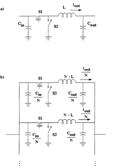
L 'out a)S1 Ci2 Cout
I
I
jout b) S1 N - L C;n S2 CoutTN
NTiout
S1 N C;n S2 Cout --NNFigure 2.3 Comparison of the power stages of a) a dc/dc converter with a single structure; and b) an equivalent converter made up of N cells.
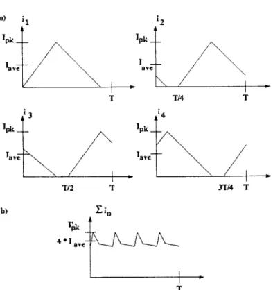
cycle, as illustrated in Fig. 2.4. Interleaving N converter cells results in a net functional
ripple frequency at the ports of the converter which is N timed the individual cell
frequency. Furthermore, it can be shown that the peak-to-peak ripple current amplitude at
the ports will be at least a factor of N times smaller then would be obtained with a single
large converter or with synchronous switching [6-9].
Due to the need for paralleled components even in a single converter design, and
considering the additional benefits provided by an interleaved design, a cellular design
Ipk aV __ T A3 Ipk 1 ave T/2 T '2 Ipk I ave T/4 T i4 Tpk lave 3T/4 T b) £in 41 ave T
Figure 2.4. Output current waveforms in a 4 cell converter with interleaved switching. a) The output of each of the 4 stages and b) the resulting interleaved output current.
considered. Using two cells would have still required using paralleled components in the
cells, and due to practical limitations the benefits of interleaving cease to accrue when
more then about 6 cells are used.
2.2.2
Effects of Number of Cells on Output Ripple
Because the converter consists of several cells, each cell can be operated in
discontinuous conduction mode and the output of the converter will still be continuous, as
illustrated in Fig. 2.4. After considering different options, the prototype converter was
designed such that the converter always operates in discontinuous conduction mode
(DCM) regardless of the voltage on either bus, and operates at the edge of discontinuous conduction at one edge of its operating voltage range. This decision was made to keep the
designed to operate at a cell switching frequency of 125 kHz. This value represents a
typical value for the operation of a dc/dc converter and was an initial assumption for the
design of the converter.
The cell inductance needed to ensure that the cell remains in DCM can be
determined as follows: at the edge of DCM the average current through the inductor,
Ia = ""'a (where Imax is the rated current for the converter), is half of the peak current in N
the cell Ipk. The peak current in a cell operating in DCM is
I - i" - "ou" .D - T (2.1) L
Assuming that the converter cell is operating at the boundary between
discontinuous and continuous (CCM) conduction modes, then the duty cycle is
D = " (2.2)
Vin
and Ipk is twice Iave (ipk = 2 -Ia,). Thus, the maximum inductance to ensure DCM is
L = (Vil -Vem) -Vout T -N (2.3)
2. Vill -I
The minimum value of
f(Vin,Vout)= (Vi - Vot. VOUt (2. 4)
Vin
can be found by solving for when either or equals zero. Since there is no
avin
NvOW
solution to the partial derivatives within the voltage ranges, the minimum value will be at
one of the edges of the voltage range. In our case the minimum is fmin = 7.63. The maximum cell inductance to ensure that the converter always operates in DCM is
.45piH -N, assuming that the cell switching frequency of 125 kHz, the maximum output
current of 68 A, and N cells are used.
Based on the inductance, bus voltages, switching frequency, number of cells, and
output current, the amount of current ripple that the converter contributes to the input or
output busses can be calculated. The waveform of the current in each cell can be
computed, then by summing the currents in each cell, the aggregate peak to peak ripple
can be found. For any given set of input parameters such as output current or inductance,
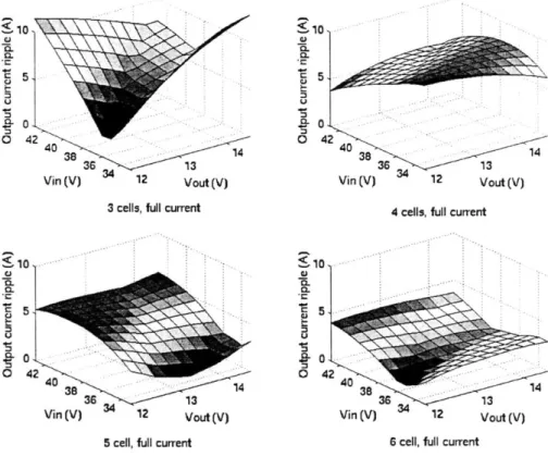
the ripple can be plotted for all combination of bus voltages. Four examples of these plots
are shown in Fig. 2.5 assuming that the cell switching frequency is 125 kHz, that the
converts are rated for 68 A, and the cell inductance is .45pH -N. The plots in this figure
help to visualize the effects of the operating conditions on the current ripple for different
V V 2 Vout()V(V) ) 12 Vout (V)
3 cells, full current 4 cells, full cunrent
S10 -10
CL
CL CL
-- 0 0
0 42 0 42
Vin (V) 12 Vout (V) Vin (V) 12 Vout (V) 5 cell, full current 6 cell, full current
numbers of cells. To further ease visualization of this relationship the data can be shown
on a two dimensional plot as in Fig. 2.6. In this figure the maximum ripple was found for
every value of V., across all possible values of input voltage and output current. With
each increase in the number of cells, the fundamental ripple frequency increases and
output peak to peak current ripple decreases. The resulting tradeoff is that increasing the
number of cells makes filtering easier, but also increases the part count and the
complexity of the converter.
2.2.3 Effects of the Number of Cells and Switch Type on
the Temperature Rise and Required Heatsink
Another major effect that the number of cells has on the system is the size of the
required heatsink. As the number of cells, N, increases, the average current per cell
decreases by a factor of N. This reduction in current causes a reduction in total
Max. amount of ripple current vs. Vout for 3, 4, 5, and 6 cells
12 -10 4 cells @500 KHz 8 0. 6 ds@S ~ iZ 2-0 12 12.5 13 13.5 14 14.5 Vout (V)
Figure 2.6 Comparison of the worst case output peak to peak current ripple as a function of cell number and output voltage across all allowed output currents. Listed also is
conduction losses in the switches if the same switches are used independent of the
number of cells. (Chapter 5 describes how to calculate the device losses and how to
choose the heatsink.) Switches with lower power losses require smaller heatsinks. Thus,
the tradeoff is that using more cells results in smaller net heat sinking but a higher part
count.
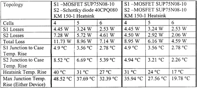
Switch selection affects the power dissipation. The three combinations of
topologies considered and shown in Fig. 2.7 result in different power losses under
different operating conditions. Also, using two MOSFETs may result in lower power
losses but will require extra control circuitry including another gate driver. Table 2.1
displays the predicted power loss and temperature rises of the converter using two
MOSFETs and a MOSFET and a Schottky diode. Both systems assume identical
heatsinks.
The prototype converter has four cells and uses the Temic SUP75N08-10
MOSFET and the International Rectifier 40CPQ080 Schottky diode as switches SI and
S1
Input Filter Output Filter
S2
b)
Input Filter Output Filter
S2
c) Si
Input Filter Output Filter
S2
Topology SI -MOSFET SUP75NO8-10 SI -MOSFET SUP75N08-10 S2 -Schottky diode 40CPQ080 S2 -MOSFET SUP75N08-10
KM 150-1 Heatsink KM 150-1 Heatsink Cells 4 5 6 4 5 6 SI Losses 4.45 W 3.24 W 2.53 W 4.45 W 3.24 W 2.53 W S2 Losses 7.28 W 5.72 W 4.61 W 4.50 W 2.92 W 2.06 W Total Loss 11.73 W 8.96 W 7.14 W 8.95 W 6.16 W 4.59 W S1 Junction to Case 4.9 *C 3.56 *C 2.78 *C 4.9 *C 3.56 0C 2.78 0C Temp. Rise S2 Junction to Case 8.52 *C 6.69 *C 5.39 *C 4.94 *C 3.21 0C 2.26 *C Temp. RiseI
Heatsink Temp. Rise 40 *C 31 *C 27 *C 31 *C 24 *C 17 *C
Max Junction Temp. 48.52 CC 37.69 *C 32.39 *C 35.94 CC 27.56 *C 19.78 C
Rise (Either Device) I I
Table 2.1 A comparison of the predicted temperature rises for two device configurations and various numbers of cells.
S2. The MOSFET/Schottky diode combination was chosen to reduce the complexity in the control. Four cells are used in the design of the converter as a compromise of the
various factors. The Thermalloy KR-150 heatsink, a model larger then the KM-150, was
used in order to ensure that if the devices are in an ambient temperature of 105 *C then
the junction temperature of the devices will not exceed 140 *C under any condition.
2.2.4 Cells Inductance and Filter Size
For a given number of cells the cell inductance used in the power converter
determines the amount of ripple that appears on the input and output busses. Figure 2.8
demonstrates this relationship for a converter with six cells.
The filters for the converter must attenuate the converter ripple. The converter
input and output ripple (ideally) has a fundamental frequency that is the switching
frequency times the number of cells. The filters must attenuate the fundamental and the
harmonics of these currents such that they meet the EMI specification. Thus, an increase
The Effect of Cell Inductance on Ripple for a 6 Cell Interleaved Converter 3 2.5-E 0. 0.5 0 L 0 0 5 10 15 20 25 30 35
Cell Inductance (uH)
Figure 2.8 The relationship between the magnitude of the ripple and the cell inductance for a six-cell converter. For every data point taken the design range of input and output voltages was examined to determine the maximum fundamental ripple component.
converter and therefore smaller filters can be used since less attenuation is needed. In the
design of the prototype converter this tradeoff was not examined; the power stage and the
filters were designed separately. EMI filter topologies and designs are discussed further
in Chapter 6.
2.3 The Prototype Converter
2.3.1 Major Components
The prototype was built in June of 1998 with the parts and parameters listed in
Table 2.2 and shown in Fig. 2.9 and Fig.2.10. The switching frequency and inductance
were chosen first. The inductance was chosen to guarantee that the converter cells would
run in the discontinuous conduction mode over the entire operating range, ensuring a
Ll in R -in C' in 4 sheUsC L Si 2 C 2 0, S2
Figure 2. 9 The layout of the prototype converter.
Power Stage
Voltage ranges See Appendix A
Maximum Current 68 A
Switching Frequency 125 kHz
Number of cells 4
Switch, S1 Temic SUP75N08-10
Switch, S2 IR 40CPQ080
Heatsink Thermalloy KR- 150
Inductor Core Philips RM 1OPA160 core with 3 turns
Inductance (per cell) 1.44 pH
Input Filter C2 80 pF Cornell Dubilier 4 X 935C2W20K C1 20 pF Cornell Dubilier 1 X 935C2W20K R .27 Q Ll 200 nH L2 20.5 pH Micrometals T157-40 core with 20 turns Output Filter C2 80 pF Cornell Dubilier 4 X 935C1W20K C1 20 pF Cornell Dubilier 1 X 935C1W20K R .220_ LI 100 nH L2 11.4 pH
Micrometals T250-40 core with 4
windings of 10 turns each
Table 2.2 Specifications and major components for the prototype converter.
R out L out
out Clou
Figure 2.10 Photograph of the dc/dc converter.
benefiting from the ripple reduction of interleaving and only requiring a single PC-board
mountable heatsink for each cell. The FET/Schottky diode combination was chosen to
reduce complexity in the control. Finally, a heatsink was chosen so as to ensure the
maximum junction temperature set for the semiconductor devices would never be
exceeded.
Once the key components were determined, the input and output EMI filters were
designed. The topology and the design algorithm for the EMI filter were adapted from
[10]. To design the filter, the input and output ripple across all operating conditions was examined and the worst-case harmonic at each frequency was computed. The filters were
designed so as to ensure that these ripple components were sufficiently attenuated to
conform to the SAE J1 113/41 Class 1 EMI specification. Additional information about
2.3.2 Control
The output voltage of a modem alternator is controlled with a feedback loop. As
the voltage on the bus falls below a temperature-adjusted reference value the alternator
will supply more current in order to recharge the battery and raise the bus voltage. Above
a certain value, however, the alternator current reaches a limit and ceases to rise. The
converter is controlled such that it will operate in a manner similar to an alternator but
with much higher accuracy and bandwidth. Figure 2.11 shows a graph of the output
voltage/output current characteristics of the converter. A maximum current, 'max, of up to
68 A can be set from a digital input. The converter provides a current that is proportional to the difference between the output voltage and a temperature-adjusted reference up to
the current limit. The proportionality constant is 170 A/V. The reference voltage is set to
14.2 V at 25 *C, with an ambient temperature adjustment of -7 mV/*C to match lead-acid
battery characteristics. Note that the output current limit for the converter is digitally
controllable between 0 and 68 A. An 8-bit digital input is provided which allows this
I &
OLt
IMAX~
I with diffrent digillinpits mnax
current limit to be set. This input is highly useful for managing the flow between the high
and low-voltage batteries.
The converter is controlled with two feedback loops. An outer loop generates a
cell current command based on the error between the output voltage and the reference
voltage. This current command is fed to the current-control loops of each cell.
The individual cells employ average current-mode control to ensure that their
average output currents track the command current from the outer loop. (Average current
was selected over peak current control or duty ratio control because it was found to result
in the lowest sensitivity of the ripple cancellation to mismatches in cell inductances.) The
average cell currents are measured across 5 mQ sense resistors in series with the cell
inductors. The error between the commanded and measured currents is used to determine
the duty ratio of the cell.
The inner control loops operate at a relatively high bandwidth. The outer loop
operates at a much lower bandwidth resulting in an overall bandwidth on the order of the
outer loop crossover frequency of 1 to 10 kHz.
The controller is also required to be stable and well behaved both with and
without a battery on the output. More details of the control will be described in [11]. For
full schematics of the prototype see Appendix C.
2.4 Test Results
The converter was tested to ensure proper operation and stable control for
operation with and without an external battery. A load step test was performed to
compare the transient response of the 14 V bus in the dual-voltage system to the nominal
the performance of the filters. The temperature rises of various components were
measured in order to estimate the accuracy of the temperature rise prediction of the
various models, used to design the converter.
2.4.1 Transient Tests
One of the transient tests preformed on the converter is a step change in load.
These transitions occur when a major load is abruptly disconnected from the bus. The
dc/dc converter can respond to this step change in current thus allowing a quick
regulation of the voltage. Careful control of such transients is especially important in a
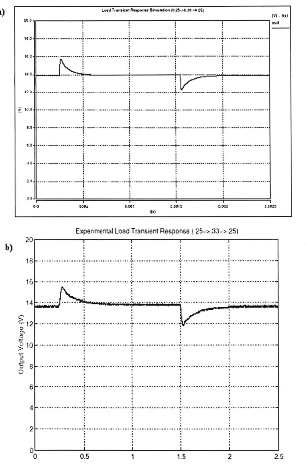
system where a 14 V battery is not used. Figure 2.12 shows a load-step transient on the
low-voltage bus of a load resistance increase from .25 i to .33 Q then back to .25 Q,
changing from 78 % to 59 % to 78 % of full load, without a low-voltage battery. Figure
2.12a is the simulated result from a Saber model, and Fig. 2.12b is the measured
transient. These results show that the performance of the converter is as expected and is
quite acceptable from a transient point of view. The voltages never exceeded the
specifications listed in Appendix A and the transients decay an order of magnitude faster
then load step transients in the conventional system under similar conditions.
2.4.2 EMI Measurements
The conducted EMI on the input and output busses were measured and compared
to the SAE J1 113/41 specification. The results of the tests are shown in Fig. 2.13. In both
cases the conducted EMI exceed the specified limits for frequencies less then 3 MHz.
This result was due to the fact that the models used to design the input and output filters
... ... ... ... ... ... ... ... 144. ... ---I . ... ... ... ... ... ... I ... ... ... . ... ... ... ... ... I'C . ... ... ... ... ... 4a . ... % ... ... ... ... .20 . ... ... ... ... ...
00 sow C.WI5 O.DGZ
Expenmental Load Transient Response
... . ... .... . .. .... .. . ... . . .. . .. . .. . . .. .. . . . ....% ... ... ... ... ... ... .. . . . . . . . .. . .. . .. . . .
...
.. . . . . . . .. . . .. . . . . . . .. .... ... ... ... ... . . . .. .. . ... . ... ... . ... . . . .. . ... ... . . .. ... .. . . ... ... . .. . . . .. . .. . . .. . .. . . . . .. . . .... . . . . ... ... ... ... ... . ... ... ... ... . ... ... ... ... ... 20 14 12 10 S 83 4 2 a) 0 0 0.5 1 1.5 2 2.5Figure 2.12 Transient response of the output voltage (in Volts) to a step in resistance on the low voltage bus without an output battery a) the simulated response b) the measured response. Along the time axis each division is .5 n-dlliseconds
a) 90 70 EMI limit (dB AV) s0 30 0 b) 90 70 EMI limit (dB IV) 50 30 0 6 12 is 24 30 6 12 Frequency (MHz) 18 24 30
Figure 2.13 The measured conducted EMI on the prototype a) input bus b) output bus at the rated power level.
described in Chapter 6) was developed for use in the CAD optimization program.
Nevertheless, the performance of the converter was found to be acceptable for test
purposes, i.e. the EMI interference did not adversely affect any other systems. D-LMT FAIL
i...
... ... ... ... .... - ..e
.. ... *.e.*. . ... ."..... ... ...
.-.. '---... .... - - Class -1 EAI specifications ---. ... .... . . ... ... ... ... ... . ... .. .. ... ... .... D-LMT FAIL - a . ... ... ... . .. .. ... . .. .. ., . . ... .. . ... .-- --- --- .--- . .---.- ... ... L ... Clss 1 EMI specifications---'---...-.---- ... . . .. ....
2.4.3 Thermal Measurements
A major design criteria for most of the components in the converter is a limited maximum temperature. In order for the heatsink and other components to be properly
chosen the power losses of the major components and resulting AT's must be accurately
calculated. Through thermal testing of the prototype converter, the actual temperature
rises of key components within the converter were compared to the predicted values in
order to test the validity of the models used.
For the thermal tests the converter was operated at an output power of 560 W. The
temperature rise of the converter cell inductor centerpost and the heatsink were measured
to be 13.3 *C and 11.9 *C, respectively. The outer case of the diode has a temperature
that is 3.9 *C higher than the heatsink. The calculated temperature rise of the converter
cell inductor is 13.7 *C. The thermal model of the heatsink and both devices, shown in
Fig. 2.14, predicts the temperature rise of the heatsink to be 12.3 *C. The measured
temperature rises for the converter inductor and the heatsink were close to the estimated
temperature rises, implying that the calculated power losses of the elements in the power
stage were accurate.
2.5
Conclusions
Several objectives were met by the development of the prototype converter. The
design and construction has helped to elucidate a number of tradeoffs and hidden issues
within the design. The tradeoffs identified include the effects of the number of cells on
system performance and the relationship between the cell inductance and filter size. The
Power lossSl \1 l82 W l5. Rjc .8"C/W 13.7 Rcs .8"C/W 2C 70C Power lossS2 4.66 W RJc 14. Rcs .4"C/W 17.*'C 12.31"C Rsa l.9 C/W
Figure 2.14 The thermal model of the heatsink and devices used in the prototype converter running at the reduced rating of 560 W. Rjc are the thermal resistances of the devices listed in Table 2.2. R, is the thermal resistance of the sil pads used. R,. is the thermal resistance of the heatsink.
the CAD optimization package. The converter has also proven useful in a variety of dual-voltage automotive research projects that include load flow studies and transient analysis.
Chapter 3
TimCAD Architecture
A wide range of design possibilities exists for a dc/dc converter in the dual-voltage application. The converter can be constructed from a single power stage or any
number of paralleled power stages. Within the power stage design, a wide range of
switching frequencies and ripple ratios are feasible, and the power stage can be
constructed from a tremendous variety of component types. Many topological variations
are possible as well. Because of this large design space and the tight interrelation of many
of the design choices, identifying the converter designs that best meet the design
objectives is extremely difficult in practice.
TimCAD is a computer-aided design and optimization tool that allows the design
space to be rapidly explored, and the most optimal design approach to be identified. It
also allows the effects of system parameter variations on the price, weight, and volume of
an optimized converter to be easily determined. This chapter describes the structure of the
TimCAD package and how it is used.
3.1 Optimization
There has been some previous work on computer-aided optimization of power
electronics. In [12], an optimization routine is coupled with a circuit simulator to select
parameters for a power converter filter. The objective function to be minimized is a
The circuit simulator ACSL is used to predict the ripple performance of a design, while a
deterministic outer loop searches for the objective function minimum.
In [13] the joint optimization of the converter structure and control behavior is
formulated as a constrained optimization problem and solved using a numerical
optimization procedure. The structural objective of the optimization is formulated in
terms of converter losses or efficiency, which are based on simplified closed-form
calculations [14], while the control cost is based on a formulation of the control effort and
performance. The authors apply this approach to the design of a buck converter, where
the plant design parameters are the converter inductance and capacitance, with other plant
parameters fixed. A major disadvantage to this approach is that it requires a very detailed
mathematical formulation of the optimization problem.
In [15], computer-aided optimization of a three-phase inverter is considered. The
objective function of the optimization is formulated in terms of efficiency or temperature
rises. Analytical expressions for converter losses and temperature rises are developed and
used for the necessary calculations. The optimization is done via a stepped search across
two design parameters (gate resistance and gate drive voltage) with all other design
choices fixed.
While having a number of distinct aspects, the existing investigations have a
number of important characteristics in common. First, in each case, only a very small
number of parameters are searched over, meaning that only a small fraction of the entire
design space is explored. It is not clear to what extent the optimization techniques and
problem formulations extend to a more extensive optimization. Second, all of the
components. For example, [12, 13] search for optimized inductance values, but there is
no tie to actual component design or consideration of actual component non-idealities. This makes it difficult to optimize for quantities such as price, weight, and volume, and
does not address many of the issues found in an actual design. Finally, all of these
investigations focus primarily on the computations and formulation aspects of
optimization. However for a CAD optimization tool to be useful across a large design
space and to address component implementation, user interface and data management
issues become very important. It is the authors' belief that these issues need to be
addressed in a fully functional optimization tool.
The TimCAD program explores the design space to identify the converter design
or set of designs that best minimize a cost function that is the weighted sum of converter
price, weight, and volume. The design variables considered by the program include the
number of interleaved cells, the cell switching frequency and ripple ratio, input and
output filter topologies and designs, and a wide variety of component types. The program
designs the converter with specific parts, each with its own price, weight, volume, and
operating characteristics. Detailed models are used to very accurately predict the system
behavior with these specific parts. The output of the program thus consists of converter
designs that are composed of available components and have well-defined performance
characteristics.
The optimization program uses a Monte Carlo design approach. The program
chooses random starting points in a user-defined design space and designs converters that
meet user-defined specifications. After designing a large number of converters across the
properties and designs are the most desirable. The program can be reconfigured to
examine local minima in the design space to further refine the search.
3.2
Program Structure
TimCAD is divided into five sections as shown in the block diagram in Fig. 3.1.
These five sections are the user interface, the control loop, the database, the design
algorithm, and the device models.
3.2.1 User Interface
The user interface of TimCAD is dialog based, i.e., the interface is made up
exclusively of dialog boxes. The toolbar and the menu of the main window can call up
any of these dialog boxes. There are three main types of dialog boxes in TimCAD: parts,
control, and results. For every major component of the converter there exists a parts
User Interface
Edit Configure
Data the Program
Results Control E~c~lia Control Loop Database Loop Design Device initias Paraeen 0;Conditions System Info DeviceDesign Models ffects on System
dialog box. The parts dialog box provides the ability to examine or edit the properties of
those parts within the database.
The control dialog boxes, Configuration and EMILimits, allow the user to set
options that will control the design algorithm or set design guidelines for several of the
components. These options include the range of allowable current ripple, the number of
cells, the maximum power loss of a component, the
Q
of the filters, and many other options.The results dialog boxes, Results and Cost, are able to manipulate the output of
the program. The Results box, as seen in the screenshot of Fig 3.2, displays all the
necessary information about the design of a dc/dc converter. The records accessed from
this dialog box are ranked based on a cost function. The cost function is a specified
weighted average of the price, weight, and volume of the converter.
3.2.2
Control Loop
The control loop is the main element in the program which regulates how the
design space is searched. Between any two successive designs of the converter many
different variable can change. The control loop controls the program by determining
which of these designs to use on each successive design of the converter. The control
loop uses a Monte Carlo design algorithm to randomly select from a number of design
parameters and components that are provided to the design algorithm. The design space
considered and the number of iterations used are key factors in the control loop, and can
both be changed through the use of the Configuration Dialog Box.
To search the design space rapidly, TimCAD actually uses a multi-layer control
;Stad ?yMicrosot Word -PrototyP... 09 TIMCAD -Mowwt DeveL '"Unied -TIMCAD I p 2:08PM
Figure 3.2 Screenshot of TimCAD
controlling the power stage design. An inner control loop designs multiple sets of input
and output filters (again using the Monte Carlo methods) for each power stage generated
by the outer control loop. The filters with the lowest weighted sum of price, weight, and volume are then chosen for the design of the converter. The number of outer loop
iterations (which are the most computationally expensive) can then be reduced since the
fast inner loop will design the optimized filters on every iteration of the outer loop.
3.2.3 Design Algorithm
The design algorithm is the section of the program that designs the converter
based on the parameters provided by the control loop. The control loop of the program
frequency, cell ripple ratio, filter topology and the selection of several components. The
design algorithm uses these values as initial conditions and determines essential values of
the design, chooses components to ensure proper operation of the converter, and makes
sure a valid design is achieved. The relationship between the control loop and the design
algorithm is shown in Fig. 3.3. To generate information necessary for the design of other
parts of the converter, the design algorithm uses models of the converter components. For
example, the models for the switches are used to calculate the power loss in the devices,
which is necessary for the design of the heatsink. If a component can not be found to
adequately meet one of the specifications, then the iteration is declared invalid and the
Outer Control Loop Choose number of cells Choose ripple ratio Choose switching frequency Choose both switches
Power Stage, Design Algorithm Calculate power loss in switches
Design heatsink
Design converter inductor
Inner , Control Loop Choose filter type
Choose capacitor
for both input and output filter
Filter Stage , Design Algorithm
Design Input Filter
Design Output Filter y iterations
x iterations
Figure 3.3 Relationships between the control loop and the design algorithm. The outer loop calls the power stage design algorithm. After the power stage is designed the inner control loop runs and the filter stage is designed. The inner control loop iterates y times and the outer control loop iterate x times.
control loop chooses another point in the design space to analyze. Once a design is
successfully completed, the program will calculate the total price, weight and volume of
the valid design and save this record in a database.
3.2.4 Device Models
An object of code exists for every component used in TimCAD. Within each of
these objects is a model for that component describing the necessary aspects of its design
and use. When supplied with data from the design algorithm, the code for the component
will calculate and relay to the design algorithm all the relevant information about the
chosen component.
3.2.5
The Database
The program uses a Microsoft Access database to store all essential data. The
database is comprised of 23 tables separated into two different files. The Parts List file
contains a table for every component used in TimCAD with all the properties needed for
that component. Three other tables in the Parts List file, EMILimits, Configuration], and
Coiflguration2, store information on user-defined variables for the converter. In the table EMI Limits, each record contains the EMI limit and frequency that define each corner of the EMI specification for up to 30 megahertz. All the variables used to configure
TimCAD (listed in Table 3.1) are stored in the Configuration] and Configuration2 tables.
The configuration data is separated into two tables because the number of fields in any
database that interacts with another program is limited to forty. Along with other
configuration data, the Configuration2 table also stores the constants for the cost function
and the information determining which filter topologies to consider.
Field Description
Vin min Minimum voltage on the input bus
Vin max Maximum voltage on the input bus
Vout min Minimum voltage on the output bus
Vout max Maximum voltage on the output bus
Switching frequency min Minimum switching frequency for the power devices
Switching frequency max Maximum switching frequency for the power devices
Switching frequency step The increment of possible switching frequencies
Ripple Ratio min Minimum ripple ratio for one cell at nominal voltages
Ripple Ratio max Maximum ripple ratio for one cell at nominal voltages
Ripple Ratio step The increment of possible ripple ratio
Linear distribution Determines whether the possible values of ripple ratios is linearly or
exponentially distributed
Number of cells min Minimum number of cells to consider
Number of cells max Maximum number of cells to consider
Filter 1 Specs Q min For Filter type 1, the minimum Q to consider
Filter 1 Specs Q max For Filter type 1, the maximum Q to consider
Ambient Temperature The ambient temperature that the converter must be designed for
Max Temperature The maximum temperature of any device in the converter
verage Current The maximum average current that the converter must deliver to the low
voltage bus
FET gate drive current The average current that the gate drivers use to switch the MOSFETs
Capacitor max The maximum number of capacitors it place in parallel at the ports of each cell
PC board Price The price of the PC board in $/cm^2
Rcs Thermal resistance of material between the case of the device and the heatsink
Outer loop Iterations The number of runs TimCAD will perform
Inner loop Iterations The number of filter designs that will be examined for every outer loop
iteration
Continuous Mode Allows designs for continuous mode operations
Discontinuous Mode Allows designs for discontinuous mode operations
Switch 2 - FET Allows a MOSFET to be used as the second switch
Switch 2 - Diode Allows a Diode to be used as the second switch
Switch 2 - Schottky Diode Allows a Schottky Diode to be used as the second switch
Output filter simple windings The output EMI Inductor has a simple or complex winding
Output filter max power loss The maximum power loss acceptable in the output EMI inductor
Input filter simple windings The input EMI Inductor has a simple or complex winding
Input filter max power loss The maximum power loss acceptable in the input EMI inductor
Master control price Price for the control that controls the entire converter
Cell control price Price for the control that controls an individual cell
Master control weight Weight for the control that controls the entire converter
Cell control weight Weight for the control that controls an individual cell
Master control volume Volume for the control that controls the entire converter
Cell control volume Volume for the control that controls an individual cell
Max allowable price Maximum price for valid designs
7Max allowable weight Maximum weight for valid designs
Max allowable volume Maximum volume for valid designs
Use Max Values Toggles if maximum values limits are used
Again the results from the design must be split into four tables to limit the number of
fields per table to 40. The Results table contains the price, weight, and volume
information about the converters. The ResultsB table contains information about the
power stage whereas ResultsC and ResultsD store information about the filter stages. For
every results table there are also two tables created to store saved results. TimCAD can
copy the current results of any optimization process to either of these saved positions.
3.3 Program Objects
TimCAD is an object-oriented program. An object-oriented program can be
viewed as a collection of separate subprograms, or objects, that are linked to other objects
to create the full program. There are three main templates for the objects used in
TimCAD: CRecordset, CDialog, and CDocument.
3.3.1 CRecordset Objects
The CRecordset class is the object that directly interfaces with the database. Each
table used in the database has a corresponding CRecordset associated with it. Code within
these classes deals with the components associated with the table they represent. For
example, the CRecordset associated with MOSFETs, named CFETSet, contains the code
that models the MOSFET. When designing the converter, the code will send the CFETSet
object several parameters and this object will calculate the power loss of the device. The
code responsible for modeling all the components are fully contained in these CRecordset
classes. Along with code specific to the component, these objects contain the code that
link the program to the individual database tables. This code that interacts with Microsoft
3.3.2 CDialog Objects
CDialog classes are the interface elements between the user and the program. For
every dialog box there is a CDialog class that controls its operation. This class reads and
writes information from the CRecordset class associated with the CDialog class. This
class controls all the user interactions such as displaying and editing the database records.
3.3.3 The CDocument Object
The most prominent class in the program is the CDocument class, even though
only one CDocument object, named CTIMCADDoc, exists in the program. This object
contains the design algorithm and the outer control loop. When the optimization
algorithm is started this object receives the command and proceeds to start the outer loop.
The program will then carry out the commands in the design algorithm and will interface
with the device models in the CRecordset objects as needed.
3.4 Program Operation
3.4.1 Installing TimCAD
To install TimCAD on any Windows 95 or 98 computer, one moves the files
TIMCAD. exe, Parts List. mdb, and Results. 11db onto the computer. The next step is to use
the ODBC program to make the database accessible to various other programs. From the
Start Menu choose Settings, then Control Panel. Then, start the ODBC program. On
the User DSN tab choose Add and then select the Microsoft Access Driver from the Create New Data Source box. On the ODBC Microsoft Access 97 Setup box choose
Select and find the Parts List.mdb file and choose OK. Then repeat this process for the