HAL Id: hal-02401217
https://hal.archives-ouvertes.fr/hal-02401217
Submitted on 24 Nov 2020
HAL is a multi-disciplinary open access
archive for the deposit and dissemination of
sci-entific research documents, whether they are
pub-lished or not. The documents may come from
teaching and research institutions in France or
abroad, or from public or private research centers.
L’archive ouverte pluridisciplinaire HAL, est
destinée au dépôt et à la diffusion de documents
scientifiques de niveau recherche, publiés ou non,
émanant des établissements d’enseignement et de
recherche français ou étrangers, des laboratoires
publics ou privés.
Electric field enhancements due to space charge in thin
polyimide film
Kunihiko Tajiri, Hirotaka Muto, Flora Carrasco, Laurent Berquez, Didier
Marty-Dessus, Marie-Laure Locatelli, Sombel Diaham, Virginie Griseri,
Thierry Lebey, G. Teyssedre
To cite this version:
Kunihiko Tajiri, Hirotaka Muto, Flora Carrasco, Laurent Berquez, Didier Marty-Dessus, et al..
Electric field enhancements due to space charge in thin polyimide film.
Conference on
electri-cal insulation and dielectric phenomena, Oct 2019, RICHLAND, United States.
pp.
781-784,
Electric field enhancements due to space charge in
thin polyimide film
K. Tajiri, H. Muto
Advanced Technology R & D Center, Mitsubishi Electric Corporation, 8-1-1, Tsukaguchi-Honmachi, Amagasaki, Hyogo 661-8661, Japan
F. Carrasco, L. Berquez, D. Marty-Dessus, M. L. Locatelli, S. Diaham, V. Griseri, T. Lebey, G. Teyssedre
LAPLACE (Laboratoire Plasma et Conversion d'Energie), Université de Toulouse, CNRS, INPT, UPS;118 route de Narbonne, F-31062 Toulouse, France
Abstract- Polyimide (PI) is widely used in film form as a passivation material for power semiconductor devices of Si, SiC, GaN, etc. The magnitude of the electric field at the edge termination area of these semiconductor devices is becoming higher and higher due to the increase of operational voltage and /or demand for shrinking the edge termination area to increase device active area. Hence it is concerned that space charge accumulation in the encapsulation and passivation material affects the insulation performance of those devices. In this report, space charge distribution and electric field enhancement associated with the charge accumulation have been investigated for thin PI film with thicknesses of about 20 μm, using Laser Intensity Modulation Method (LIMM). It is shown that the enhancement factor of the internal electric field (the maximum internal electric field divided by the applied field) in PI film is negligibly small (less than 1.1) for applied fields less than 10 kV/mm. However, it can reach much higher like 1.4 at higher applied field like 25 kV/mm. This result implies that electric field at edge termination area should be carefully designed under such an operational electric field as is the case of SiC devices.
I. INTRODUCTION
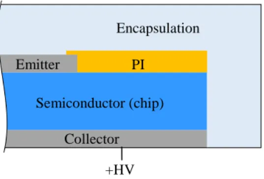
In recent years, high voltage electronics and power electronics applications have emerged needing the use of wide bandgap semiconductor (SiC, GaN…). In these devices, thin polymer films have been widely used as passivation film to protect device surfaces. Particularly, polyimide (PI) is of great interest owing to its excellent thermal and electrical properties and its easy processing. Some of the most important applications of these materials films are as inter-level dielectric insulators and as electronic device surface passivation [1], the typical image of PI layer at the edge surface of semiconductor chip is shown in Fig. 1.
Space charge is generally reported as a triggering mechanism for the degradation of insulators [2], and considered as a cause of the decrease of electrical breakdown voltage of those polymer films. Furthermore, the space charge could degrade semiconductor leakage current characteristics by strengthening the electric field into semiconductor substrate region. Reliability tests of IGBT devices under accelerated conditions have been reported in [3][4] showing that the degradation (increase) of leakage current of the device is caused possibly by the formation of space charge on the
Fig. 1. Termination structure of chip
surface at semiconductor edge termination area. The space charge caused the carrier inversion layer of the silicon depletion region just beneath the junction termination, resulting in the increase of the leakage current.
Earlier reports featuring space charge in PI [5-7] addressed the processes indirectly e.g. through charging current measurements or directly as with pulsed electroacoustic (PEA) method with relatively thick films (125µm) [5]. We recently introduced the Laser-Induced Modulation Method (LIMM) [8] for investigating space charge in thin PI films with few µm in thickness [9]. Some studies have been performed through charge accumulation measurement in silicone gel using PEA method [10], and insulation resistance test by applying external electric field on the semiconductor edge termination area simulating space charge existence [11]. Although the cause of leakage current increase of the device has been estimated by space charge, no sufficient study has been done based on actual charge accumulation measurement in PI or interface between PI and encapsulation under an electric field at semiconductor edge area.
The space charge investigation using the same PI film under extremely higher DC stress, close to breakdown voltages, from 25 to 125 kV/mm has already been reported and discussed with DC conductivity trend in [12][13]. In the present paper, experimental studies of the space charge dynamics in thin PI films in more moderate electric fields under 25 kV/mm are presented using the LIMM. The influence of space charge on the device performances is also discussed. PI Collector Semiconductor (chip) +HV Emitter Encapsulation
II. EXPERIMENTAL DETAILS A. Samples
The Metal-Insulation-Semiconductor (MIS) structure is used as a sample. Polished <100> Si-substrates, of a few hundred micrometers in thickness and 3 inches in diameter, highly doped with phosphorus (n-type, resistivity between 0.001 and 0.003 Ω.cm) have been used as a bottom electrode. The PI-layer is laid onto the Si wafer by spin-coating. The top electrode of gold is deposited onto the upper surface of PI with 150 nm in thickness and 16 mm in diameter by sputtering. A layer of nickel is deposited on the bottom face of the substrate to avoid oxide formation and ensure an ohmic contact. A final PI film thickness of about 20 µm was obtained as measured by a mechanical profilometer. All the samples were dried at 150°C in an air-oven for 7 days before the experiment to avoid any influence of water on the PI dielectric response.
B. Space Charge Measurement Methods: LIMM
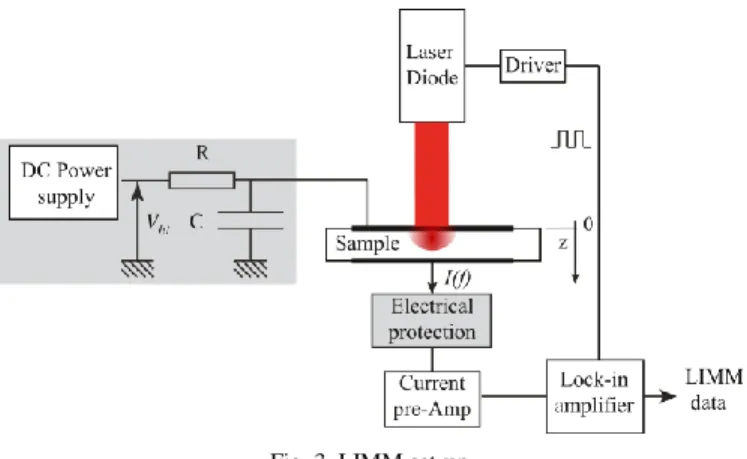
The LIMM is a thermal based method dedicated to the characterization of space charge dynamics in thin dielectric films. Fig. 3 shows a schematic view of LIMM set-up. The thermal gradient created by laser beam induces periodical and local expansions that lead to relative charge displacement regarding to the electrodes within the irradiated volume. The penetration depth of the thermal perturbation can be chosen by the different modulation frequencies. The lower the frequency is, the deeper the thermal modulated zone. In the LIMM, the tested sample, which is placed in a measuring cell and with its both surfaces coated with opaque electrodes, is exposed to the laser irradiation. The pyroelectric current due to coupling of thermal modulation and space charge is pre-amplified and extracted from the noise by the way of a lock-in amplifier. A mathematical deconvolution technique is then performed to compute space-charge and internal electric field distributions from the current-frequency data [14].
The polarization steps consist in applying a DC electric field from 2.5 to 25 kV/mm with positive or negative polarity. The corresponding positive or negative DC voltages are applied on the top electrode of the sample in air at room temperature, whereas the Si substrate is grounded as shown in Fig. 2. After each polarization step, a depolarization process is performed by short-circuiting the sample.
Fig. 2. Schematic view of samples
Fig. 3. LIMM set-up
A cumulative protocol is applied for successive voltage steps on the sample as shown in Fig. 4. Volt-on and volt-off steps of each 30 min each are applied on the sample from 2.5 to 7.5 kV/mm, then volt-on/off steps continues from 10 to 25 kV/mm for 60 min each, with the steps of 2.5 kV/mm. LIMM measurements are performed throughout the whole protocol, with every 10 min scanning of 63 frequency points from 10 Hz to 10 kHz.
III. EXPERIMENTAL RESULTS
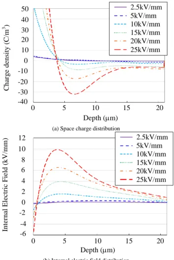
Fig. 5 shows space charge and internal electric field distributions at different applied electric fields by DC stress from 2.5 to 25 kV/mm with positive polarity on top electrode. LIMM results shown here are obtained in the last 10 min sequence of volt-on step at every DC field. A build-up of negative charges is observed at the depth of a few m from the surface electrode as the applied DC field increases. A positive charge is also observed at the vicinity of surface electrode; the charge amount increases as the applied electric field rises (Fig. 5(a)). It has to be noted that the space charge magnitude contains some errors close to top electrode surface compared to the deeper area. According to the charge distribution described above, a positive peak of internal electric field is observed at a few m depth from the electrode surface, which increases with the applied electric field (Fig. 5(b)).
Fig. 4. LIMM measurement protocol with a positive polarity
Au PI NiSi Si substrate (n-type) HV (positive or negative) GND Ap p lied elec tr ic field ( k V/m m ) 0 200 400 600 800 1,000 Time (min) 30 0 20 10
Fig. 6 shows space charge and internal electric field distributions at different applied external DC field for negative polarity with the same magnitudes as for positive polarity shown in Fig. 4. Under negative polarity, positive and negative charges are observed close to surface electrode and few µm in depth from the surface electrode, respectively, similar to the case of positive polarity shown in Fig. 5, which leads to the positive peak of internal electric field at few µm in depth from the surface. In addition to that, positive charge build-up is also observed deeper in polyimide, which leads to the negative local peak of internal electric field as shown in Fig. 6(b).
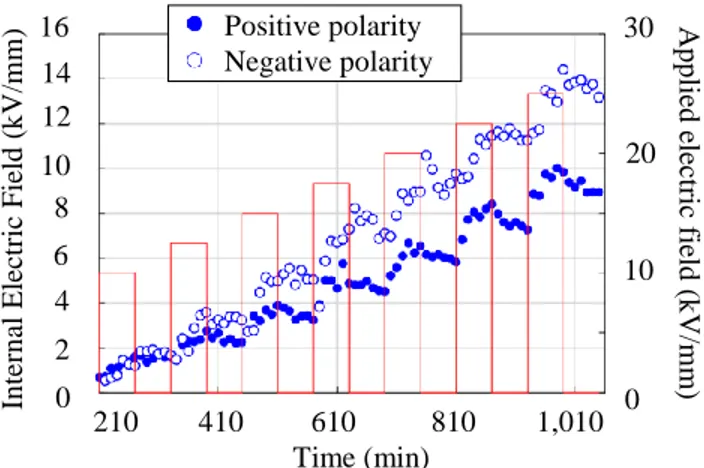
Fig. 7 shows the peak magnitudes of internal electric field for the whole LIMM protocol from 2.5 to 25 kV/mm under both polarities. The residual field values seem to saturate in every steps of volt-on during 60 min of field application. The decaying trend of peak value is observed during short-circuit after polarization, but it is very slow. The magnitude remains almost the same level during 60 min of short-circuit showing almost no charge relaxation at room temperature.
(a) Space charge distribution
(b) Internal electric field distribution
Fig. 5. Space charge and internal electric field distribution with different DC fields at positive polarity
(a) Space charge distribution
(b) Internal electric field distribution
Fig. 6. Space charge and internal electric field distribution with different DC fields at negative polarity
IV. DISCUSSION
As a distinctive result, a large build-up of negative charge is observed at a depth of a few m from the top electrode, under both polarities, and the peaks magnitude increases with the DC field. The cause of the large negative charge accumulation is presumed to be electron injection from the Si substrate under positive polarity, and likewise negative charge injection from the surface gold electrode under negative polarity. This second hypothesis was confirmed in [12] where electron injection from the top electrode was clearly limited when the top electrode was aluminium and where native alumina (formed between the top electrode and the PI-layer) acts as an electronic barrier. Under a negative polarity, the observed positive charge in the vicinity of the Si is assumed to be injected from Si substrate.
To clarify the degree of space charge accumulation due to external DC electric field, the peak values of internal electric field are plotted in Fig. 8, extracted from Fig. 5(b) and 6(b).
C h ar g e d en sity ( C /m 3 ) 40 20 0 -20 -40 Depth (m) 0 5 10 15 20 2.5kV/mm 5kV/mm 10kV/mm 15kV/mm 20kV/mm 25kV/mm 50 30 10 -10 -30 In ter n al E lectr ic Field ( k V/m m ) 10 8 6 0 -6 -4 0 5 10 15 20 Depth (m) -2 4 2 2.5kV/mm 5kV/mm 10kV/mm 15kV/mm 20kV/mm 25kV/mm 12 C h ar g e d en sity ( C /m 3 ) 100 20 -60 -100 Depth (m) 0 5 10 15 20 -20 60 2.5kV/mm 5kV/mm 10kV/mm 15kV/mm 20kV/mm 25kV/mm -140 In ter n al E lectr ic Field ( k V/m m ) 8 0 -12 -8 0 5 10 15 20 Depth (m) -4 4 12 16 2.5kV/mm 5kV/mm 10kV/mm 15kV/mm 20kV/mm 25kV/mm
Fig. 7. The magnitudes of space charge and internal electric field under whole LIMM measurement
During polarization under positive polarity, the field is reinforced by the positive peak, whereas the enhancement by the negative peak is considered under negative polarity. Values are not presented for 2.5 and 5 kV/mm under negative polarity because peaks of internal electric field are not confirmed or negligibly small. It is confirmed that the peak values of the internal electric field begin to increase rapidly when the applied field exceeds 10 kV/mm for both polarities. To evaluate the impact of charge accumulation inside PI more clearly, enhancement ratio of electric field is also plotted in Fig. 8. The large enhancement of electric field is confirmed for DC stress higher than 10 kV/mm. If the device is used under electric field of few kV/mm around passivation layer, it is not largely affected due to the charge accumulation measured at this level. However, the effect of field enhancement due to space charge accumulation should be considered in PI films used in passivation layer on device if the design field is much higher than a few 10 kV/mm.
Fig. 8. Peak value of positive internal electric field (filled circle) and enhancement ratio of the peak (open square) versus applied electric field
IV. CONCLUSION
Space charge distributions in PI thin films have been evaluated by LIMM under DC electric fields in the range from ±2.5 to ±25 kV/mm using MIS structure sample. It was shown that the enhancement factor of the internal electric field (the maximum internal electric field divided by the applied field) in PI film is negligibly small (less than 1.1) in the field range of less than 10 kV/mm. However, it can reach much higher like 1.4 at higher applied field than 25 kV/mm. These results imply that the electric field at edge termination area should be carefully designed in the case of such an operational electric field as is the case in SiC devices.
In this report, the space charge behavior is discussed only in the case of dried samples. To elucidate the effect of space charge on the actual device, further investigation using models representing actual insulation structure, including an influence of environmental conditions of high temperature or high humidity, is necessary.
REFERENCES
[1] S. Zelmat, M.-L. Locatelli, T. Lebey, and S. Diaham, « Investigations on high temperature polyimide potentialities for silicon carbide power device passivation », Microelectron. Eng, vol. 83, pp. 51-54, 2006. [2] G. Mazzanti, G. C. Montanari, and L. A. Dissado, « Electrical aging and
life models: the role of space charge », IEEE Trans. Dielectr. Electr. Insul., vol. 12, pp. 876-890, 2005.
[3] N. Tanaka et al., “Robust HVIGBT module design against high humidity,” in Proc. PCIM Europe 2015, pp. 368-373, 2015.
[4] Y. Kitajima et al., “Lifetime estimation model of HVIGBT considering humidity,” in Proc. PCIM Europe 2017, pp. 353-358, 2017.
[5] K. Kaneko, R. Shiomi, Y. Suzuoki, T. Mizutani, H. Shiota, and H. Muto, « Effects of electrode material on injection and space charge formation in polyimide », Proc. IEEE Internat. Conf. Solid Dielectrics, pp. 518‑ 521, 2007.
[6] G. M. Sessler, B. Hahn, and D. Y. Yoon, « Electrical conduction in polyimide films », J. Appl. Phys., vol. 60, pp. 318‑ 326, 1986.
[7] T. Liang, Y. Makita, and S. Kimura, « Effect of film thickness on the electrical properties of polyimide thin films », Polymer, vol. 42, pp. 4867-4872, 2001.
[8] A. Petre, D. Marty-Dessus, L. Berquez, and J.-L. Franceschi, « A comparison of different mathematical treatments for solving the inverse problem in focused laser intensity modulation method », Jap. J. Appl. Phys., vol. 43, p. 2572-2579, 2004.
[9] M.-L. Locatelli, C. D. Pham, S. Diaham, L. Berquez, D. Marty-Dessus, et G. Teyssedre, « Space charge formation in polyimide films and polyimide/SiO2 double-layer measured by LIMM », IEEE Transactions on Dielectrics and Electrical Insulation, vol. 24, no 2, p. 1220 1228, avr. 2017.
[10] H. Shiota, and H. Muto, “Space charge behavior and electrical conduction of silicone gel” in Proc. Symposium on Electrical and Electronic Insulating Materials and Applications in Systems, pp. 49-52, 2006.
[11] A. Yamatake et al., “New technology for evaluating insulation reliability of terminal of power semiconductor chip,” in Proc. IEEJ, p.157, 2017. [12] F. Carrasco et al., «Assessment of the High Field Behaviour of
Polyimide Films: Experimental Methods and Impact of Electrode Material », Proc. ISEIM 2017, pp.122-125, 2017.
[13] F. Carrasco et al., «Effect of film thickness and electrode material on space charge formation and conductivity in polyimide films », in Proc. IWIPP, 2019, to be published
[14] S. B. Lang and D. K. Das Gupta, « Laser intensity modulation method: A technique for determination of spatial distributions of polarization and space charge in polymer electrets », J. Appl. Phys., vol. 59, pp. 2151-2160, 1986. In ter n al E lectr ic Field ( k V/m m ) 10 8 6 0 4 2 12 210 410 610 810 1,010 Time (min) Ap p lied elec tr ic field ( k V/m m ) 20 0 10 30 Positive polarity Negative polarity 14 16 0 12 10 8
Applied electric field (kV/mm) 6 4 2 -30 -20 -10 0 10 20 30 In ter n al elec tr ic field ( k V/m m ) E n h an ce m en t r atio 1.0 1.8 1.6 1.4 1.2 Internal electric field