HAL Id: hal-02994864
https://hal.archives-ouvertes.fr/hal-02994864
Submitted on 8 Nov 2020
HAL is a multi-disciplinary open access
archive for the deposit and dissemination of
sci-entific research documents, whether they are
pub-lished or not. The documents may come from
L’archive ouverte pluridisciplinaire HAL, est
destinée au dépôt et à la diffusion de documents
scientifiques de niveau recherche, publiés ou non,
émanant des établissements d’enseignement et de
SiC MOSFETs soft and hard failure modes: functional
analysis and structural characterization
Frédéric Richardeau, François Boige, A. Castellazzi, V. Chazal, A. Fayyaz, A.
Borghese, Andrea Irace, G. Guibaud
To cite this version:
Frédéric Richardeau, François Boige, A. Castellazzi, V. Chazal, A. Fayyaz, et al.. SiC MOSFETs soft
and hard failure modes: functional analysis and structural characterization. 2020 32nd International
Symposium on Power Semiconductor Devices and ICs (ISPSD), Sep 2020, Vienna ( virtual ), Austria.
pp.170-173, �10.1109/ISPSD46842.2020.9170094�. �hal-02994864�
SiC MOSFETs soft and hard failure modes:
functional analysis and structural characterization
F. Richardeau
1, F. Boige
1, A. Castellazzi
2, V. Chazal
3, A. Fayyaz
4, A. Borghese
5, Irace
5, G. Guibaud
3 1LAPLACE, University of Toulouse, CNRS, Toulouse INP, UPS, Toulouse, France
2
Solid-State Power Processing (SP2) Lab, Engineering Faculty, Kyoto University of Adavanced Science, Japan
3ITEC Lab, THALES, Toulouse, France
4
PEMC Group, University of Nottingham, Nottingham, UK
5DIETI, University of Naples “Federico II”, Italy
[email protected]: [email protected]; [email protected]
Abstract—This paper discusses first the discriminating
phenomena yielding either a fail-to-short or fail-to-open circuit signature in 1200 V SiC power MOSFETs undergoing short-circuit electro-thermal stress. Since fail-to-open behavior is of particular relevance to the application, the paper goes on to propose a benchmarking of a number of commercial devices, identifying a single product which offers consistent fail-to-open characteristics with bias voltages up to at least 50% of nominal rating. For that particular device, a thorough functional and structural characterization is presented. In particular, it is shown that: the gate current is an effective monitor of ensuing degradation under short-circuit stress and can be used to assess damage accumulation, as well as the reversible or permanent nature of device degradation; fail-to-open signature is associated with degradation of the gate-structure, with the creation of short-circuits between the gate and source terminals in regions relatively far away from the active cells and not involving the field oxide. The findings are relevant to application of both discrete devices and multi-chip power modules, including multiple parallel connected dies.
Keywords—Silicon carbide; SiC MOSFETs; short-circuit robustness; fail-to-open.
I. INTRODUCTION
Silicon carbide (SiC) power MOSFETs are rapidly gaining increasing relevance in large market applications, including harsh operation and equally reliability sensitive environments, such as automotive or avionics. A key robustness requirement in such domains, particularly in the case of electric drive applications, is short-circuit (SC) withstand capability. A substantial body of literature has already been produced on the subject, pointing out potential criticalities in this respect, when transitioning from silicon (Si) transistors to SiC ones (see [1-4], for instance). In particular, the studies in [5] have pointed out the existence of a twofold SC failure mode, depending on the rate of temperature increase: a soft one, characterized by the device failing as an open circuit drain to source (Fail-To-Open behavior, FTO) and a hard one, in which the transistor fails as a short-circuit drain to source (Fail-To-Short behavior, FTS). The two different behaviors are exemplified in the results of Fig. 1 a): the former features a collapse of the gate-source
a)
b)
Fig. 1: short-circuit current ID and VDS, (top) and VGS
(bottom), a); summary of SC failure mode (FTO or FTS) for different commercial devices at different VDS, b).
voltage to a value well below the threshold voltage (as a result of damage in the gate structure, the gate-source resistance after damage is lower than the external drive gate resistance, RGS <<
RG,EXT), which practically results in the device turning off the
device; the latter features a shorting of the drain-source terminals, with drain current, ID, thermal runaway and collapse
of the drain-source voltage, VDS. The specific failure mode is of
great relevance for the application, with a clear preference for FTO type transistors. Indeed, in contrast to FTO, the FTS mode typically implies: a) the fast discharge of energy storage components (e.g., capacitors), with oftentimes explosion-like characteristics and a possible failure propagation typically for a module device where chips are close to each other ; b) loss of functionality of the whole circuit in the case of parallel multi-chip architectures, either discrete or module based.
A preliminary screening on commercial 1.2 kV-rated MOSFETs delivered the results in Fig. 1 b): today a single manufacturer could be identified, whose device consistently performed as FTO for VDS values up to 50% rated voltage,
which is a representative application requirement [6]. Because of its application interest, that device was considered further in detail. a)
b) c)
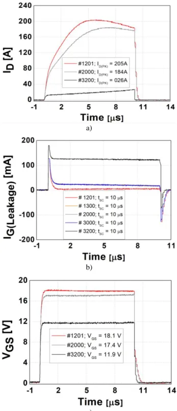
Fig. 2: Experimental results for SC tests with varying pulse durations: ID, a); VGS, b); IG,LEAK, c). A drop in VGS is
noticeable (circle) from about 10 s, at which moment IG,LEAK features a steeper increase.
a)
c)
Fig. 3: Experimental results for repetitive SC test with “short” pulse widths: ID, a); IG,LEAK, b). Though the device
characteristics are clearly severely degraded, no relation can be detected with a modification of the gate structure characteristics under these stress conditions.
II. DEVICE STRESS AND DEGRADATION MONITORING:
FUNCTIONAL CHARACTERIZATION
The gate leakage current, IG,LEAK, is an effective monitor of
FTO behavior. Past work reported no damage accumulation and device aging for pulse widths below a minimum value, which could be related to a critical IG,LEAK value [7]. So, in this
work, first, tests were carried out to identify such critical pulse-width, tPW,CRIT. The results of Fig. 2 show: the SC drain
current, ID, a); the gate-source voltage, VGS, b); IG,LEAK, c), for
the device subjected to pulses of different duration. Here, VDS=600 V in all tests. During the pulse, at about time=10 s,
IG,LEAK shows exponential increase onset, which, according to
the results presented in [7] and physically analyzed and modeled in [8] as a Schottky emission current, was retained as the tPW,CRIT for the device under test (DUT) here.
The pulse width was then halved and repetitive stress was applied: Fig. 3 a) shows degradation of the saturation characteristics after thousands of pulses; however, that was not found to be related to any degradation at gate level, as the results of Fig. 3 b) clearly shows. On the other hand, increasing the pulse width yields very different results, Fig. 4: the drain current is still degraded, a), but that is now clearly due to damage of the gate-structure, manifest in the form of substantial IG,LEAK value increase, on an accelerated basis
between #3000 and #3200 cycles , Fig. 4 b), and subsequent decrease, as a result of a low value series gate resistance in the transistor driving path, of the bias voltage applied across the gate-source terminals, Fig. 4 c).
III.STRUCTURAL CHARACTERIZATION
The results are interpreted on the basis of two different failure mechanisms intervening, depending on the pulse width: for “short” pulses (<tPW,CRIT) only reduced saturation current is
manifest (Type 1 degradation), possibly caused by degradation of the chip metallization and subsequent VGS de-biasing [2; 9];
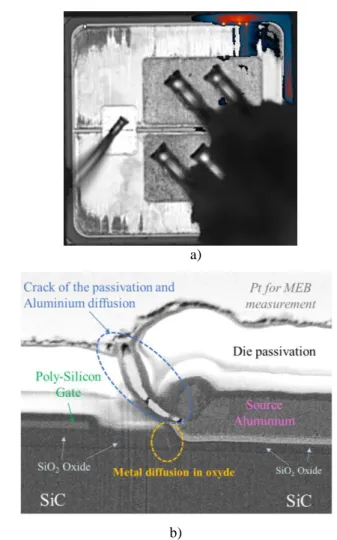
for “long” pulses, gate structure aging is evident (Type 2 degradation). The latter is caused by cracks around the inter-layer dielectric (ILD) triggered by the high difference in thermal expansion between the top Al and the SiO2 and
formation of metallic paths in the gate-source ILD, caused by the top Al melting at the edge of the chip during the short-circuit, as presented in Figs. 5 a) and b) [6]. The region of major degradation and thus leading to eventual failure was observed to change on the device surface, but it was always located near the border of the active area, where terminations of various type are present and where geometrical singularity appears between the peripheral gate distribution ring and the interdigital ramifications fingers, Figs. 6 a) and b). However, the failure mechanism remained the same, even in the proximity of active cells, Fig. 6 c), which can be reasonably assumed to be the locations reaching highest temperatures.
IV.CONCLUSION
SiC power MOSFETs exhibit some key differences with Si MOSFETs and IGBTs. In particular, their features-set implies higher electro-thermal stress levels during short-circuit. On top of that, the present level of technology maturity is still associated with a greater spread in the value of some of the
main device electro-thermal parameters, such as threshold voltage and on-state resistance. So, rather uneven degradation in parallel multi-chip structures is a likely occurrence. The
a)
b)
c)
Fig. 4: Experimental results for repetitive SC test with “long” pulse widths: ID, a); VGS, b); IG,LEAK, c). In this
case, the change in device characteristics is strictly related to degradation of the gate, as manifest by the significant increase in gate current value.
ability to ensure a soft (FTO) type of failure ensures the capability to still operate the module, even in the presence of a single die failure, enabling for instance, so-called “home-hopping” system level operation mode in critical equipment such as automotive or avionics. Studies have already been undertaken to steer and control the occurrence of the desired FTO event in a single chip, without compromising the controllability of other parallel connected devices [10, 11]. A permanent gate leakage current of several mA is a salient precursor, easy to detect and monitor by the gate-driver circuit to reduce ageing and, for instance, trigger a supervisory system to stop operation at a suitable time to replace one or more devices in the system, before any failure occurs.
REFERENCES
[1] A. Castellazzi, T. Funaki, T. Kimoto, T. Hikihara, Short-circuit tests on
SiC power MOSFETs, 2013 IEEE 10th International Conference on
Power Electronics and Drive Systems (PEDS), 22-25 April 2013, Kitakyushu, Japan.
[2] A. Castellazzi, A. Fayyaz, L. Yang, M. Riccio, A. Irace, Short-circuit
robustness of SiC Power MOSFETs: Experimental analysis, 2014 IEEE
26th International Symposium on Power Semiconductor Devices & IC's (ISPSD), 15-19 June 2014, Waikoloa, HI, USA.
[3] A. Castellazzi et al., SiC power MOSFETs performance, robustness and technology maturity, Microelectronics Reliability Volume 58, March 2016, Pages 164-176
[4] G. Romano et al., Short-circuit failure mechanism of SiC power
MOSFETs, in Proc. 2015 IEEE 27th International Symposium on Power
Semiconductor Devices & IC's (ISPSD), 10-14 May 2015, Hong Kong, China.
[5] G. Romano et al., A Comprehensive Study of Short-Circuit Ruggedness
of Silicon Carbide Power MOSFETs, IEEE Journal of Emerging and
Selected Topics in Power Electronics, Vol. 4, N. 3, Sep. 2016, pp. 978 – 987.
[6] F. Boige et al., Ensure an original and safe “Fail-to-Open” mode in SiC
MOSFET devices in extreme short-circuit operation, Microelectronics
Reliability (88–90) 2018, 598-603.
[7] C. Chen et al., Study of short-circuit robustness of SiC MOSFETs,
analysis of the failure modes and comparison with BJTs,
Microelectronics Reliability 55 (2015) 1708–1713
[8] F. Boige et al., Physical Origin of the Gate Current Surge During
Short-Circuit Operation of SiC MOSFET, IEEE Electron Device Letters, vol.
40, no. 5, pp. 666-669, May 2019. doi: 10.1109/LED.2019.2896939 [9] V. Smet et al., Ageing and Failure Modes of IGBT Modules in
High-Temperature Power Cycling, IEEE Trans. on Ind. Electr., vol. 58, no.
10, pp. 4931–4941, Oct. 2011.
[10] F. Boige, A. Fayyaz, A. Castellazzi, F. Richardeau, S. Vinnac,
Short-circuit robustness of parallel SiC MOSFETs andfail-safe mode strategy,
European Power Elecrtonics and Applications 2019 - IEEE ECCE Europe, Sep 2019, Genoa, Italy.
[11] A. Castellazzi, A. Fayyaz, R. Kraus, SiC MOSFET Device Parameter
Spread and Ruggedness of Parallel Multichip Structures, Materials
Science Forum, 2018.
a)
b)
Fig. 5: Micrograph of MOSFET (bare-die top view) showing localized IG,LEAK increase, a); Scanning electron
microscope (SEB) image of a device focused ion beam (FIB) microsection after destructive test, b).
a)
Failure analysis of the failure mode in FTO
SiO2Oxide Passivation SourceAl SiC Poly-Silicon Gate SiO2Oxide SourceAl Metal/poly contact Metal reflux Gate ring b)
Fig. 6: Micrographs of MOSFET (bare-die top view) showing movement of localized IG,LEAK increase, a); SEB
image of device FIB microsection confirming the failure mechanism attribute to ILD, b) (the right hand-side image is a zoom of the area highlighted on the left hand-side one).