HAL Id: tel-00825830
https://tel.archives-ouvertes.fr/tel-00825830
Submitted on 24 May 2013HAL is a multi-disciplinary open access archive for the deposit and dissemination of sci-entific research documents, whether they are pub-lished or not. The documents may come from teaching and research institutions in France or abroad, or from public or private research centers.
L’archive ouverte pluridisciplinaire HAL, est destinée au dépôt et à la diffusion de documents scientifiques de niveau recherche, publiés ou non, émanant des établissements d’enseignement et de recherche français ou étrangers, des laboratoires publics ou privés.
magnétron et stratégie de dopage à l’azote pour des
applications photocatalytiques dans le visible
Houssam Fakhouri
To cite this version:
Houssam Fakhouri. Dépôt de couches minces de TiO2 par pulvérisation magnétron et stratégie de dopage à l’azote pour des applications photocatalytiques dans le visible. Génie des procédés. Univer-sité Pierre et Marie Curie - Paris VI, 2011. Français. �NNT : 2012PAO66343�. �tel-00825830�
THESE DE DOCTORAT
Présentée
À L’UNIVERSITÉ PIERRE ET MARIE CURIE Spécialité
Génie des procédés et technologies avancées Présentée par :
Houssam FAKHOURI
Pour obtenir le grade de
DOCTEUR de L’UNIVERSITE PIERRE ET MARIE CURIE (Paris-FRANCE)
Thin film deposition of pure and doped TiO
2
by RF
magnetron sputtering for visible light photocatalytic
and optoelectronic applications
À soutenir le 28 septembre 2012
Encadrement :
Mme. Farzaneh AREFI-KHONSARI Professeure, LGPPTS, UPMC-Sorbonne Universités M. Jérome PULPYTEL Maître de conférences, UPMC-Sorbonne Universités
Rapporteurs :
Mme. Nadhira BENSAADA LAIDANI Senior Scientist Researcher, FBK, Trento, Italie M. Laifa BOUFENDI Professeur, (GREMI), Université d’Orléans
Examinateurs :
M. Mehrdad NIKRAVECH Professeur, (LSPM-CNRS) Université de Paris 13 Mme. Pascale MASSIANI Directeur de Recherche-CNRS, (LRS),
UPMC-Sorbonne Universités
Invité :
M. Hubert CACHET Directeur de Recherche-CNRS, LISE, UPMC-SorbonneUniversités
Three different ways to dope nitrogen into TiO2 by means of RF reactive sputtering was
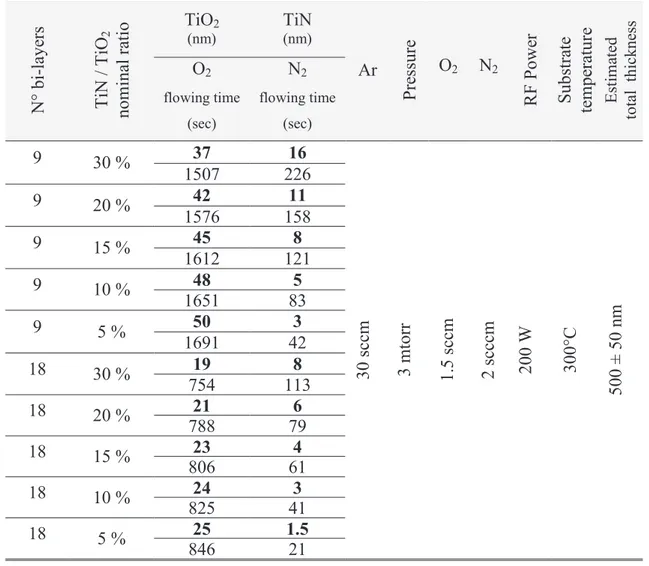
compared, and the structural, optical, and photo-active performance of these materials were explored. First, multi-layered thin films of TiO2 and TiN were prepared by sputtering a titanium
target and alternating oxygen and nitrogen reactive gases in the deposition chamber. The total thickness of each multi stack was kept constant while the overall composition of the films (TiN to TiO2 ratio) was varied between 5% and 30% and the number of TiN/TiO2 bi-layers was
increased from 9 to 45. Secondly, we prepared N-TiO2 by introducing oxygen and nitrogen
reactive gases simultaneously during the depositions. The ratio of oxygen to nitrogen was systematically changed in order to control the concentration of nitrogen incorporation into the films between 0% and 6%. Finally, we prepared TiN thin films and oxidized them at different temperatures and for several time intervals. X-ray photoelectron spectroscopy showed that nitrogen was successfully doped into all of the TiO2 films in substitutional and/or interstitial
sites depending on the deposition conditions. The variance in the concentration and position of the nitrogen doping had a significant effect on the optical, structural and photoactive properties of the three types of N-TiO2 films. The parameters of sputtering deposition were optimized
using both plasma diagnostics and Design of Experiments. This study has shown the desirable ability to control several important physical and chemical characteristics of N-TiO2 films, with
considerable promise for many applications.
Key words: TiO2 thin film, Nitrogen doping, photocurrent, bi-layer, RF sputtering, photo
catalyze, TiN, Oxidation.
Résumé
Nous avons comparé trois méthodes différentes de dopage de TiO2 à l'azote par pulvérisation
cathodique, et avons exploré les propriétés structurelles, optiques et la photo-activité de ces matériaux. Tout d'abord, des films minces successifs de TiO2 et TiN ont été créés par
pulvérisation d'une cible de titane et en alternant les gaz réactifs d’oxygène et d'azote dans l'enceinte de dépôt. L'épaisseur totale de chaque multicouche a été maintenue constante tandis que nous avons fait varier la composition globale des films (rapport TiN/TiO2) entre 5% et 30%
et le nombre de des couches TiN/TiO2 entre 9 à 45. Deuxièmement, nous avons préparé des
couches homogènes de N-TiO2 par l'introduction simultanée des gaz réactifs d’oxygène et
d'azote au cours du dépôt. Nous avons systématiquement fait varier le rapport azote/oxygène afin de modifier d’une façon contrôlée la concentration de l'azote incorporé dans les films de 0% et 6%. Enfin, nous avons préparé des couches minces de TiN et les ont fait subir l’oxydation à des températures différentes pendant plusieurs intervalles de temps. Les mesures d’XPS ont montré que l'azote a été dopé avec succès, dans tous les films de TiO2, dans les sites
substitutionnels et/ou interstitiels en fonction des conditions de dépôt. La variance de la concentration et la position du dopage à l'azote avait une influence significative sur les propriétés optiques, structurelles et photo-actives des trois types des films de TiO2 dopés. Les
paramètres de dépôt par pulvérisation ont été optimisés grâce à des diagnostics du plasma et à un Plan d’Expériences. Cette étude a montré que nous pouvons modifier d’une façon contrôlée et à souhait plusieurs caractéristiques physiques et chimiques importantes des couches de N-TiO2, qui pourront avoir un grand potentiel pour de nombreuses applications.
Mots clés: couche mince TiO2, dopage d’azote, photo-courant, bi-couche, RF pulvérisation
Introduction Général
Les semiconducteurs sont des matériaux clés autant pour la production d’énergie solaire que la photodégradation des polluants contenus dans l’eau. Les couches minces à base de dioxyde de titane (TiO2) sont couramment utilisés dans les cellules photoélectrochimiques
de par leur capacité à photodissocier l’eau, permettant ainsi à la production d’hydrogène. Depuis les années 70, de nombreux travaux se sont orientés vers le développement et l’optimisation de nouveaux matériaux possédant notamment une énergie de gap compatible avec les applications photocatalytiques.
Le TiO2 peut dégrader de nombreux polluants organiques dissouts dans l’eau
sous l’action des rayonnements UV. Cependant, à cause de sa largeur de bande d’énergie interdite importante (3,2 eV), ce matériau n’absorbe que très peu la partie visible du rayonnement. De nombreux efforts ont donc été fournis pour permettre l’absorption du spectre visible. En particulier, la stratégie la plus répandue consiste à diminuer l’énergie de gap par dopage.
Les trois caractéristiques principales pour permettre au TiO2 d’avoir une bonne activité
dans le visible sont i) d’introduire des états dans la bande d’énergie interdite permettant ainsi l’absorption de photons visibles, ii) le maximum de la bande de valence (VB) ainsi que les niveaux d’énergie du dopant doivent se trouver au-dessous du potentiel d’oxydation de l’eau (H2O/O2) alors que le minimum de la band de conduction (CB) doit se trouver au dessus du
poteltiel de reduction (H2/H2O), iii) les niveaux d’énergie du dopant doivent se recouvrir
suffisamment avec les bandes de TiO2 afin de permettre un transfert rapide d’électrons.
Le TiO2 dopé à l’azote a suscité beaucoup d’attention grâce à ses bonnes propriétés
photocatalytiques, mais les nombreuses contradictions rapportées dans la littérature font encore l’objet de débats à l’heure actuelle. Dans cette thèse, nous nous sommes focalisé sur la préparation et la caractérisation de différentes couches de TiO2 dopées azote (TiO2 :N) par
pulvérisation réactive magnétron en vue d’applications liées au traitement de l’eau.
Cette thèse est constituée de 6 chapitres. Dans le premier chapitre, les processus élémentaire entrant en jeu dans la photocatalyse sont décrits, ainsi que l’état de l’art sur l’élaboration des couches de TiO2 dopées et non dopées. Le second chapitre est dédié aux
diagnostics du plasma par spectroscopie optique d’emission (OES) et par sonde de Langmuir, afin de comprendre le procédé de dépôt par pulvérisation. Les phénomènes d’empoisonnement de la cible et d’hystérèse ont été particulièrement étudié, car ces phénomènes peuvent changer fondamentalement les conditions opératoires et ainsi les
propriétés des dépôts. Ce chapitre est la base de connaissance principale permettant de sélectionner les paramètres de dépôt étudiés dans les chapitres suivants.
Dans le troisième chapitre, la méthodologie des plans d’expérience a été utilisé afin d’avoir un large aperçu de l’effet des paramètres du procédés sur les caractéristiques physico-chimiques et sur les propriétés photoactives des films de TiO2 dopés N. L’autre avantage des
plans d’expériences consiste à pouvoir faire varier simultanément différents paramètres afin d’observer leurs interactions ; dans ce chapitre la pression et la composition du gaz plasmagène constituent les paramètres étudiés.
Les derniers chapitres sont dédiés à l’étude de trois strategies différents pour produire des films de TiO2 dopés azote, permettant ainsi d’avoir une bonne compréhension du rôle de
la localisation de l’azote dans les films (insertionel ou substitutionnel) dans la maille de TiO2,
ainsi que de la morphologie des films et de la concentration en azote.
Dans le chapitre 4 nous allons étudier le dépôt de couches de TiOxNy possédant
différentes morphologies et différentes concentrations en azote en introduisant simultanément l’azote et l’oxygène dans l’enceinte de pulvérisation. Des caractérisations poussées par XPS et DRX ont permis de démontrer qu’il est possible de contrôler la localisation de l’azote dans la maille par l’intermédiaire des paramètres du plasma.
Dans le chapitre 5, une nouvelle stratégie jamais rapportée, à notre connaissance, dans littérature a été mise en place. Cette nouvelle approche consiste en l’élaboration de multi-couches de TiO2/TiN. Les résultats obtenus ont permis de démontrer que les hétérojonctions
présentent dans le film permettent une bonne séparation des porteurs de charges et ainsi de meilleures propriétés photoactives.
Enfin dans le chapitre 6, des couches minces de TiN ont été deposes puis oxydées par recuit dans l’air afin de produire des couches de TiO2:N. Les résultats obtenus montrent que
cette stratégie est très intéressante pour produire des couches photoactives dans le visible, bien qu’elle nécessite des traitements post-plasma des dépôts. Dans ce chapitre, les contradictions que l’on trouve dans la littérature sur l’oxydation de TiN seront aussi mises en évidence.
General Introduction
Semiconductors have received considerable attention as a potential solution for clean energy and for photocatalytic degradation of hazardous pollutant in the environment. Titanium dioxide (TiO2) thin films are used in photoelectrochemical cells, because they have
the ability to photo-dissociate water and produce photocurrent for hydrogen production. Since 1970, many efforts have been made to explore suitable materials and to optimize their energy band configurations for photocatalytic applications.
TiO2 can photodegrade many organic pollutants dissolved in water via UV irradiation.
However, due to its large band gap TiO2 absorbs visible light poorly, and thus has been
ineffective for visible-light photocatalysis. Many attempts have been made to improve the photocatalytic activity of TiO2 under UV and/or visible light irradiation. In particular, the
main strategy was to decrease the band gap energy of TiO2 (around 3.2 eV), in order to absorb
visible light, i.e. energies in the range of 1.6–3.0 eV, particularly at 2.5 eV, which corresponds to the solar maximum emission intensity.
Three main characteristics are required to achieve good visible-light activity for TiO2,
i) doping should introduce states within the band gap that could be excited by absorbing visible light, ii) the conduction band (CB) minimum and the dopant states must be above the H2/H2O reduction level to ensure photoreductive activity, and the valence band (VB)
maximum should be lower than H2O/O2 oxidation level, iii) sufficient overlap between the
doping energy states and band states of TiO2 is required, in order to provide a fast transfer of
the photo-excited carriers to the surface within their lifetime.
Nitrogen doped TiO2 has received significant attention, but its photoactivity results,
reported in the literature, have yielded many contradictions and the efficiency of nitrogen doping sites is still under debate. In this thesis, we will focus on the preparation and characterization of nitrogen doped TiO2 (TiO2:N) by RF reactive magnetron sputtering for
water purification and water splitting. The thesis is composed of six chapters.
In the first chapter, the fundamental processes involved in photocatalysis as well as the state of the art for intrinsic and doped TiO2 will be described.
The second chapter is dedicated to plasma diagnostic by Optical Emission Spectroscopy (OES) and by Langmuir probe, in order to understand the plasma deposition process by sputtering. Target poisoning and hysterisis phenomena will be particularly highlighted, because they can dramatically change the process conditions and thus the properties of the coatings. This chapter is the main basis to select the deposition parameters for the different studied films in the following chapters.
In the third chapter, the Design of Experiments (DoE) methodology will be used in order to have an overview about the effect of the different parameters on the physico-chemical characteristics and the photoactivity of N doped TiO2 films. The advantage of using DoE is to
be able to study, simultaneously, the effect of variation of different plasma parameters and to highlight the synergic effects of the most important parameters in the case of the reactive sputtering, which were the pressure and gas composition in the reactor.
The last chapters are dedicated to three different strategies to produce N doped TiO2
films, that allowed us to have a good overview about the role of both nitrogen doping sites (interstitial or substitutional) in the lattice of doped titania as well as the effect of the morphology and the doping concentration on the nitrogen incorporation and the resulted photoactivity.
Chapter 4, is devoted to the deposition of homogeneous TiOxNy films with different
morphologies and nitrogen concentrations by the dual gas sputtering process. Extensive studies of the films by XPS and XRD will demonstrate that it is possible to control the position of nitrogen doping (interstitial or substitutional) by controlling the main plasma parameters.
In chapter 5, a new strategy never reported in the literature before will be developed. This new approach consisted in the production of TiO2/TiN multi-bi-layers. The results will
highlight the fact that the heterojunctions obtained in the films can increase the charge separation effect, and thus increase the photoactive properties of the films
Finally, in chapter 6, the production of N doped TiO2 by oxidizing TiN thin films will be
presented. The results will highlight the fact that this strategy is very interesting in order to produce thin films with good photoactive properties. This chapter in particularly emphasizes the contradiction which is found in the litterature survey on the oxidation of TiN.
Chapter I
State of the art
Abstract
The utilization of solar irradiation to supply energy or to initiate chemical reactions is already a well established idea. If a semiconductor such as titanium dioxide (TiO2) is
irradiated with light greater than the band gap energy, excited electron–hole pairs are generated that can be utilized in many applications such as solar cells to generate electricity, chemical processes to create or degrade specific compounds, or in producing self cleaning surfaces using the photo-induced super hydrophilicity of TiO2 films.
TiO2 shows relatively high activity and chemical stability under ultraviolet light
(l<387nm), the energy of which exceeds the band gap (3.2 to 3.3 eV) of the anatase crystalline phase. The development of photo-catalysts exhibiting high reactivity under visible light (l> 400 nm) should allow the main part of the solar spectrum to be used, even under the poor illumination of interior lighting. Several approaches for TiO2 modification have been
proposed such as metal-ion implantation using transition, noble, alkaline and rare metals, reduced TiOx photo-catalysts, non-metal doped-TiO2 (N, S, C, B, P, I, F), composites of TiO2
with another semiconductor having a lower band gap energy (i.e. CdS, WO3, …), sensitizing
TiO2 with dyes, and TiO2 doped with up conversion luminescence agents.
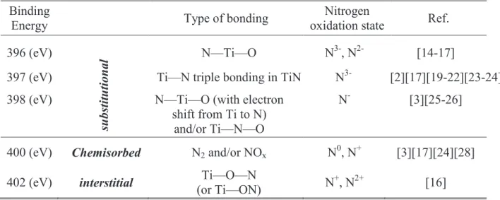
The morphology effect is less investigated in literature especially in the studies of TiN oxidation to get N-doped or even pure TiO2. Nitrogen can occupy substitutional (N–Ti–O or
Ti–O–N) and/or interstitial (π* character NO) sites in the titania lattice. This can introduce discrete nitrogen energy states levels at 0.14 eV and 0.73 eV above the top of the valence band, for substitutional and interstitial nitrogen, respectively. Up to now there is no evident explication how to control the presence of one with respect to the other, also, what is the contribution of each nitrogen site on the photo-activity of the doped titania.
In particular, this thesis will primarily focus on the role of nitrogen doping on the photo-activity, morphology, structural, optical, and electronic properties of TiO2. Three methods
utilizing RF sputtering will be used in order to create N-doping within TiO2; the oxidation of
TiN thin films, creating bi-layered TiO2/TiN films, and the direct dual gas deposition of
TiON. By optimizing the experimental conditions, it is possible to achieve nitrogen doped TiO2 coatings with a desired stoichiometry, concentration and position of doped nitrogen in
the TiO2 lattice. Such coatings can then be used to elucidate the role of substitutional and
Résumé
L'utilisation de l'irradiation solaire pour l'approvisionnement en énergie ou pour initier des réactions chimiques est une idée, déjà, bien établie. Si un semi-conducteur, tel que le dioxyde de titane (TiO2), est irradié par une lumière dont l’énergie est plus grande que
l'énergie de bande gap, des paires électron-trou sont générés dans l’état excité, ces paires photo-générés peuvent être utilisés dans de nombreuses applications telles que les cellules solaires (photovoltaïques) pour produire de l'électricité, les processus chimiques afin de créer ou de dégrader des composés spécifiques, ou en produisant des surfaces autonettoyantes à l'aide de la super hydrophilicité photo-induite des couches minces de TiO2.
TiO2 montre une photo-activité relativement élevée ainsi qu’une stabilité chimique
sous la lumière ultraviolette (l <387nm) dont l'énergie dépasse la largeur de la bande optique (bande gap) de la phase cristalline anatase (3.2 à 3.3 eV). Le développement de photo-catalyseurs présentant une forte activité sous la lumière visible (l> 400 nm) devrait permettre d’utiliser la partie principale du spectre solaire, même sous le mauvais éclairage interne. Plusieurs approches ont été proposées afin de modifier le TiO2, telles que l’implantation
ionique et le dopage par des métaux de transition, les éléments nobles, les alcalins et les terre –rares. Par ailleurs on trouve une littérature abondante sur le TiO2 dopé par les non
métaux (N, S, C, B, P, I, F), les composites de TiO2 avec d’autres semi-conducteurs ayant
une plus faible énergie de gap (CdS, WO3, ...), la sensibilisation de TiO2 avec des colorants,
de TiO2 dopé avec un agent de conversion de luminescence, ou la formation des structures
réduites de TiOx (x<2).
L'effet de la morphologie de TiO2 est moins étudié dans la littérature en particulier
dans les études du phénomène d'oxydation de TiN pour obtenir le TiO2 dopé-N ou même le
TiO2 pur. L'azote peut occuper des sites substitutionnel (N–Ti–O et Ti–O–N) et / ou
interstitiel (π* correspondant à N—O) dans le réseau de TiO2. Ce qui introduirait des états
d’énergie discrets, lié à l’azote, situé à 0.14 eV et 0.73 eV au dessus de la band de valence pour l’azote substitutionnel ou interstitiel, respectivement. Jusqu'à maintenant, il n'y a pas eu d'explication claire pour contrôler la présence de l’un ou l'autre, ou encore pour mettre en évidence la contribution de chaque site d'azote sur l’activité photo-induite de dioxyde de titane dopé-N. Cette thèse se concentrera principalement sur le rôle du dopage à l'azote sur l’activité photo-induite, la morphologie, la structure, et les propriétés optiques et électroniques de TiO2. Trois méthodes basées sur la technique de pulvérisation cathodique RF seront
utilisées afin de doper N au sein de TiO2, l'oxydation des films minces de TiN, la réalisation
d’un film mince composé d’un assemblage de plusieurs dépôt des bi-couches de TiO2/TiN, et
enfin par le dopage traditionnel en pulvérisation réactive en utilisant le couple de gaz réactifs d’oxygène et d’azote pour déposer directement les couches de TiON. En optimisant les paramètres expérimentaux, il a été possible de contrôler d’une façon très fine, dans le cas du
dopage des couches de TiO2 avec l’azote, la stœchiométrie, la concentration et
positionnement de l’azote dans la structure de TiO2. Ces couches donc vont servir pour
élucider l’effet de dopage par azote en substitutionnel et/ou interstitiel sur l’activité photo-induite des couches de TiO2 dopé-N.
I-1) Introduction
Photo-catalytic materials possess unique structural, optical and electronic properties that can be exploited for numerous applications and have been studied extensively for decades. The primary applications of photo-catalysis can be summarized into two major categories; (1) the photo-degradation of organic materials dissolved in water (or another liquid) and (2) water splitting via photolysis in electrochemical cells. The fundamental processes that drive the efficiency of photo-catalysts are governed by their material properties, the incident light intensity, the light frequency and the specific chemical processes of the catalytic reaction. In particular, the properties of the material that can drastically alter the performance of photo-catalysts are the electronic band gap, electron-hole pair generation, recombination dynamics, and finally the transportation of photo-generated charges. Understanding these characteristics individually and how they can be controlled is vital in designing improved and optimized photo-catalysts, which can perform more efficiently and effectively as compared to traditional materials.
The most prominent photo-catalytic material that has been studied is TiO2, due to its
non-toxicity, relative abundance, optical properties, and stability in aqueous solutions. However, TiO2 by itself can only reach a certain level of photo-catalytic efficiency due to its
fast electron-hole pair recombination time, as well as its large band gap energy which only absorbs UV light. Currently, there have been many research efforts exploring ways to improve the efficiency of photo-catalytic materials such as TiO2 by combining them with
other semiconductors or metals to increase the lifetime of the photo-excited electrons and holes, as well as to enlarge the spectral absorbance range to include visible light.
The potential for the applications of the photo-catalytic effects of TiO2 has attracted
considerable interest over the last three decades. The photo-catalytic oxidation of organic compounds in aqueous or gaseous environments has received the most attention, but there is a rapidly increase focus on the oxidation of volatile organic or inorganic compounds in the gas phase, including NOx and SOx. The photo-catalytic reduction of organic compounds and
metal-containing ions, as well as studies on cell killing and disinfection by illuminated titanium dioxide has also received increase attention.
I-2) Definitions
I-2-1) Catalysis and photo-catalysis
A catalyst is a material which accelerates the speed of a chemical reaction without being consumed at the end of the reaction. Its structure or composition can be altered during the reaction but there is no stoichiometric relationship between these alterations and the stoichiometry of the reaction. The photo-catalytic activity describes the acceleration of a catalytic reaction by light, and it is associated with the reaction rate.
Heterogeneous photo-catalysis involves photo-reactions at the catalyst surface:
a) if the process of initial photo-excitation occurs on an adsorbed molecule, which then interacts with the catalyst, the process is called photo-sensitized reaction.
b) if the initial photo-excitation takes place on the catalyst (photo-excited catalyst) which then acts on an adsorbed molecule, it is called photo-catalyzed reaction.
I-2-2) Band gap
The absorption of light is directly dependent on the band gap of the photo-catalyst, which can be explained by the band theory of solids. The band theory classifies materials by their band gap, which is the energy difference between the top of the valence band and the bottom of the conduction band electron orbitals. The valence band is also referred to as the highest occupied molecular orbital (HOMO), which is the highest orbital that an electron is naturally found in a material, while the conduction band is referred to as the lowest unoccupied molecular orbit (LUMO), because it is the next stable electron orbit that is not already occupied by an electron. The band structures for an insulator, a semiconductor, and a metal are shown in Fig.I-1 to detail the different electronic structures for these distinctively different materials.
Insulators are characterized by their traditionally large band gaps (Eg), which are what
give them their intrinsic properties of having poor electron mobility, since the conduction band and valence band are relatively far apart and thus require a large amount of energy to transfer the electrons between bands. Semiconductors have a discrete band gap that is typically much smaller than that of insulators, but is still well defined. Metals have no band gap, but instead have a continuous series of electronic bands throughout the material. This continuum of electronic bands give metals their intrinsic properties of being good electrical
conductors, because the conduction and valence bands are so close that electrons are free to move between bands with little or no energy needed.
In order for an electron to be promoted from the valence band to the conduction band level for semiconductors and insulators, it needs to be excited either thermally, electronically, or optically. If a photon with energy greater than or equal to the band gap energy of a material is incident on its surface, an electron in the valence band could absorb this photon and could be excited to the conduction band discretely and becomes a photo-carrier.
Fig.I-1: Band structures (a) for an insulator, semiconductor and metal & (b) for intrinsic, n type and p type semiconductors.
For example, with TiO2, the bulk band gap energy in the anatase phase is Eg = 3.2 eV
(Eg = 3.0 eV for the rutile phase), which is the energy between the valence band
(corresponding to the O 2p orbital), and the conduction band (corresponding to the Ti 3d
orbital). The energy Eg = 3.2 eV corresponds to a wavelength of l = 388 nm, which is in the
UV region of light.
I-2-3) Fermi level
Another similar and helpful way to characterize different electronic materials is through a description of their Fermi energy level, Ef. For a semiconductor in thermal
equilibrium at absolute zero, the Fermi level is defined as the highest filled level of electrons in the ground state. At some finite temperature above this, the electrons gain kinetic energy and can be excited into states above the Fermi level, leaving available openings below that energy (Fig.I-2). We define the Fermi function f(E) which gives the probability that a given available electron energy state (E) will be occupied at a given temperature (T). The Fermi function has the form:
[ ]
1
1
)
(
( )+
=
-kT E E fe
E
f
Eq.I-1(a)
(b)
Fig.I-2: Fermi function and Fermi level in a semiconductor as a function of temperature.Note that at hight temperature some electrons can reach the conduction band (in red colore).
The electron population depends on the product of electron density and Fermi function. The Fermi function has a finite value in the gap but electron density is zero in the gap so there is no electron population at those energies (gap). In the conduction band at 0K, there are plenty of available states but there are no electrons because the Fermi function is zero. At high temperatures, both the density of states and the Fermi function could have finite values in the conduction band, so there could be a finite electronic population in the conduction band.
I-2-3) Charge separation
When electron-hole pairs are generated by photo-excitation, they are typically separated for a finite and pre-determined amount of time that is an intrinsic property of the material, and crystalline structure of the material that is being excited. The forward and back transition rates, for electrons going to and from the conduction and valence energy bands, could be described by the equations:
[ Rf r af] f f
r
W
e
k
(
)
=
( - )/ Eq.I-2 and [ Rb r ab] b br
W
e
k
(
)
=
( - )/ Eq.I-3where the subscripts f and b denote the forward and back processes, k is the transition rate, W is the transition probability determined by Fermi’s golden rule, r is the inter-particle distance,
R and a are constants used to parameterize the distance scales of each transition and fall-off of
the electronic wave function of the states, respectively. These forward and back transition rates can help to determine the probability of finding an electron or hole in a particular state via the following relationships,
) , ( ) ( ) , ( ) (r n r t k r p r t k dt dp b f f -= Eq.I-4 ) , ( ) (r n r t k dt dn b b -= Eq.I-5
where p is the probability of finding a hole, n is the probability of finding an electron. From these relationships we can see two trends. First, the change in the probability of finding a hole is dependent on both the forward and backward transitions. This makes sense because the holes are only produced via excitation (the forward reaction), and are then consumed by the backward reaction (recombination). The other trend is for the change in the probability of finding an electron in a given state, which is dependent only on the back reaction kinetics. Again, this makes sense because unlike the photo-generated holes, the electrons are present at all times within the material. The dependence on the back reaction relates to the lifetime of both the electron and holes, because the rate with which the electrons fall back to the initial state will determine the annihilation of holes.
Since the photo-generated holes (and sometimes electrons) are the predominant driving mechanism in photo-catalysis, in type-n semiconductor, it is advantageous to keep the charges separated for as long as possible. While the intrinsic recombination time, t , is determined by the crystal structure of a material, there are several ways to increase the recombination time by changing the material properties, doping and adding other semiconductors or metals to the primary material. This process is called charge separation.
I-2-4) Efforts to enhance the charge separation
Charge separation initially occurs by photo-excitation, but can be extended by creating hetero-junctions between two materials. For instance, when silver is loaded on titania in a TiO2-Ag system (Fig.I-3 c), electrons can be excited via photon absorption in TiO2, and then
attracted to Ag due to the difference in Fermi energy levels between the semiconductor and the metal. The difference in the Fermi energy levels and the vacuum energy level characterizes the work function for each material, and is equivalent to an electric potential. The contact between the two materials creates a junction, called a Schottky barrier, where there is an appreciable difference in Fermi energy levels, and thus a difference in the work functions [1]. The difference in the work functions creates an effective electric field that
drives electrons toward the metal, and holes toward the semiconductor creating an effective charge separation.
Similarly, if another semiconductor is combined with TiO2 the differences in the
Fermi level of each material creates an electric field due to the different work functions, and also creates an effective charge separation. Using a two-semiconductor system requires the second material to have a higher work function, and thus a lower Fermi energy level than the first material, so each must be chosen carefully to satisfy these conditions. A pictorial representation of the band structure of a single photo-active material as well as a two types of hetero-structures, two semiconductors and one semiconductor and one metal loaded, are shown in Fig.1-3.
Fig.I-3: Electronic band structure for a single semiconductor, a two semiconductor system, and a semiconductor combined with a metal.
Specifically, the Fermi energy level of the secondary material (metal or semiconductor) needs to be slightly lower than that of the primary material, so that there is a difference in work functions at the junction between the two materials to create an effective electric field. When this is the case, photo-excited electrons in the conduction band of the first material have the ability to transfer to the conduction band of the secondary material (or trapped by the doping metal). This pulls the electrons away from the primary material, and keeps the photo-generated holes free for a longer period of time to continue breaking down reactants, and improve photo-catalytic performance. Effective charge separation can also be achieved through the doping within TiO2. In the case of TiO2 prepared in the amorphous state,
it has shown poor photo-catalytic activity. This can be explained by the electronic and optical properties of amorphous materials, which dictate that they have no defined band gap. That means that there can be several valence and conduction band energies, with no preference or higher density of one state of energy with respect to others. This, in effect, creates defect energy levels within a defined band gap, so that electrons can be promoted and recombine at several energy levels. With several stable energy levels that are very close together,
excited electron-hole pairs are given many opportunities to recombine, and have a shorter distance, or lower amount of energy to travel.
However, when TiO2 is prepared in the anatase, or even rutile phase, the
photo-catalytic performance has shown significant enhancement. The reduction of defects allows the electron-hole pairs to stay apart for a longer time than if there were defects. While the reduction of the latter can remove recombination and trap centers within the band gap, the electron-hole lifetime is still governed by the energy separation in the band gap of TiO2.
Doped atoms directly inserted into a host lattice, can create bonds with the host atoms, which have different strengths as compared to the initial homogeneous bonds of the host. These new bonds can change the electron/hole conductivity drastically in a local space around the defects, and create a new distribution of electronic energy levels that can keep photo-generated charges apart from each other for a longer period.
I-2-5) Charge transport
Another important characteristic property that determines the performance of photo-catalytic materials is the charge transport of photo-generated charge carriers throughout the material. Since the photo-catalytic reactions occur at the surface of the material, it is important for the photo-generated charges to be able to diffuse to the surface before recombining with each other.
There are two important factors that can affect the transport of charge throughout a material. The first factor is the crystal structure of the material. If an electron-hole pair is created within the bulk of a material, it needs to travel to the surface to complete the chemical reaction. Its path, from the bulk to the surface, is much simpler and easier if the crystal structure of the material is uniform, so that the charge carriers can transfer throughout the lattice easier. The electron mobility is determined by its mean free path, which is larger in an ordered crystal lattice than a defect heavy lattice. This is made easier from a highly ordered crystalline material, because the crystal order corresponds to stable and uniform energy levels surrounding each atom in the crystal lattice. This allows the photo-generated charge carriers to smoothly move from atom to atom by not having to change energy levels and gaining or losing energy. If the crystal structure of the material is not uniform, and has many defects, the mobile charge carriers can be trapped or recombine much more easily as they move throughout the crystal lattice
Another factor that can affect charge transport within a material is the morphology of the structure. For example, for a dense thin film, when electron-hole pairs are created within
the bulk material, their motion is determined by a random-walk mechanism. This means that once the charge carriers are generated, they move randomly throughout the thin film, and have no preference to go to the surface, or be extracted in a photo-electrochemical cell.
Fig.I-4: Schematic diagram for electron transport in 0-D and 1-D nanostructures
However, if the material is fabricated in a columnar and porous morphology, such as
O-D or 1-D nanostructures, the charge transport can be improved. An additional issue for
films with interconnected zero-dimensional (0-D) nanoparticles in charge transport, is often limited because of the lack of continuous conducting pathways, with electrons moving by a hopping mechanism due to energy barriers between particles [2]. 1-D nanostructures are expected to have improved charge transport properties compared to 0-D nanostructures [3] because of the direct conduction pathways in columns or nanorods compared to electron hopping in nanoparticle systems. A representative scheme showing the electron mobility in
0-D and 1-0-D nanostructures is shown in Fig.1-4.
In a successful utilization of 1-D nanostructures, Paulose et al. [4] demonstrated hydrogen generation utilizing 6 μm long TiO2 nanotube arrays and attained a hydrogen rate of
~ 180 mLhr-1 via photolysis.
I-2-6) Role of adsorbate electrophilicity on charge transport
For polycrystalline TiO2, it has been shown that electrons could be trapped in the
conduction band upon either thermal or photon excitation, where they reside for a long time if the temperature is sufficiently low. The conduction band is depopulated by heating the sample or by charge transfer from the conduction band to adsorbates on the surface. It has been found that efficient charge transfer occurs exclusively between the TiO2 surface and an
adsorbate molecule with an electrophilic moiety. No observable charge transfer occurred with a similar molecule with no hydrophilicity [5].
I-2-7) Reaction steps in heterogeneous photo-catalysis
When an electron is electronically excited from the valence band to the conduction band, it leaves behind a positively charged hole that is also mobile and can move throughout the bulk or surface of a material similar to the way the electrons can move around the conduction band. Both the electron and hole are used to induce the chemical reactions at the surface of the semiconductor material (Fig.I-5). Traditionally, the holes act as an oxidizing agent while the electrons act as reducing agents at the surface of the material. Because the electron-hole pair is very active and initiates most of the reactions on the surface of photo-catalysts, it is beneficial to have a high concentration of these charge carriers at the surface, and to also keep them apart for an extended period of time.
Fig.I-5: Schematic diagram for the reaction steps in heterogeneous photo-catalyse
Heterogeneous photo-catalysis is a complex process that has been the subject of significant research. As with any method including reactions in heterogeneous phases, the photo-catalytic process can be divided into five steps:
1. transfer of reactive molecules dispersed in the solution or gas phase to the catalyst surface 2. adsorption of reactive molecules on the surface of the catalyst
3. reaction on the surface of the adsorbed phase 4. desorption of products
5. elimination of products from the fluid/catalyst interface
The actual photo-catalytic reaction occurs in step 3. When a semiconductor catalyst (SC) of oxide type (TiO2, ZnO) or chalcogenide (CdS, ZnS) is illuminated by photons of
creation of electron-hole pairs. The electron-hole pairs dissociate into free photo-electrons in the conduction band and photo-holes in the valence band. Simultaneously, in the presence of a fluid phase (gas or liquid), adsorption occurs, and depending on the redox potential (or energy level) of each adsorbate, an electron transfer takes place towards molecules of acceptor behavior (A), while the positive photo-holes are transferred to the molecules of donor character (D). Once the reactants are broken down, products are formed at the surface and can be taken away, to free the valuable active surface area needed to continue the reaction effectively. Thus, an important factor in photo-catalysis is that breaking down reactants must deal directly with the diffusion of unreacted particles to the photo-catalyst surface, as well as the diffusion of the reactant products away from the photo-catalyst surface.
The other mechanism for photo-catalysis still involves the photo-generated holes, but only in a secondary manner. This mechanism supposes that the holes break down water molecules into hydrogen (
H
+) and hydroxy radicals (OH·) as follows:· + +
+
®
+
h
H
OH
O
H
2 Eq.I-6From there, the hydroxyl radicals, which have a very high oxidation potential, can break down the organic molecules:
· ·
+
®
+
R
OH
R
OH
Eq.I-7This reaction scheme is more complicated than the first and requires a two-step process to degrade the dissolved organic materials. While the first mechanism relies on the diffusion of the holes to the photo-catalyst surface as well as the diffusion of the reactants to the surface and the products away from the surface, the second scheme has several more steps. The diffusion of the holes to the surface should be the same as the first scheme, since the photo-catalyst is the same regardless of which reaction scheme we use. However, when the holes break down the water molecules into hydrogen and hydroxyl radicals, these radicals must then find the reactant molecules to break them down. Hydroxyl radicals are not very stable, and have relatively short lifetimes (<1 ms) before forming more stable products such as water or hydrogen peroxide. This scheme requires that the radicals find a reactant molecule and break it down before they become stable themselves, which is a difficult, delicate, and quick process.
Fig.I-6: Some measured characteristic time scale for primary processes in TiO2 photo-catalysis after Fujishima et al. [6].
Both of these schemes, i.e. breaking down the pollutants directly or by means of hydroxyl radicals have been used to describe the effect of active photo-catalysts to breakdown organic materials at their surface. While the exact mechanism or number of steps involved is different between the two schemes, there are some similarities that are apparent. Such similarities are that the reaction is driven primarily by the photo-generated holes, and the higher amount of surface area of the photo-catalyst will allow for more holes to reach the surface and either directly breakdown the reactant, or break down water molecules to participate in the degradation reactions. This information is vital for creating optimized photo-catalysts that can take advantage of this mechanism, and a higher performance should be seen in samples with higher surface area. Examples of some measured characteristic times for primary processes in TiO2 photo-catalysis have been collected in Fig.I-6 and in the
annexes of this chapter. [6].
The principles that govern the photo-degradation of pollutants in aqueous solutions and electrochemical water splitting are mostly the same. They include the generation of induced charges, light, and surface reactions. The differences are that the catalytic degradations are localized on the surface of the catalyst, while the electrochemical water splitting reactions transport generated electrons from the photo-catalyst to an anode material to complete the redox reactions.
Fig.I-7: Band positions of several semiconductors in contact with aqueous electrolyte at pH 1 [7]
Fig.I-7 presents the Band positions of several semiconductors in contact with aqueous electrolyte at pH=1 (see also [118]), we define the electron affinity of a semiconductor as the difference between its conductive band minimum and the vacuum energy. A solid which has more positive electron affinity is often called electron acceptor, and the one which has less positive electron affinity is called electron donor, as presented in Fig.I-7. It is useful to note that water splitting could be thermodynamically possible, on the surface of the semiconductor, if the valence band and the conduction band of the semiconductor are lower than O2/H2O
redox couple and higher than H2O/H2 redox couple, respectively. In another words, the
valence band should be more positive than
V
O HO2
2/ and the conduction band should be more
negative than
2
2O/ H
H
V
(the semiconductor bands cover the water redox voltages).I-3) Titanium dioxide (TiO
2)
I-3-1) Advantages of titania semiconductor
TiO2 has attracted significant interests for many applications, especially for its high
stability and resistivity to corrosion, availability and its low-cost production. Also, this semiconductor has a conduction band CB minimum and dopant states positions above H2/H2O
level. Sufficient overlap between the intra-gap and band states of the photo-catalyst could provide a fast transfer of photo-excited carriers to the reactive sites at the surface within their
Electron acceptor
Electron donor
lifetime. On the other hand, effective absorption of photons over the visible range (i.e., 1.6– 2.8 eV) could be realized with modified TiO2 (doped or defected titania), and it is possible to
get a high surface area with a high density of localized states involving energetic electrons between the conduction band and valence band especially in the case of powders and porous thin films.
I-3-2) Different crystalline structures of TiO2
Titanium dioxide (TiO2), also known as titania, is an important photo-catalytic material that
exists as two main polymorphs, anatase and rutile having tetragonal coordination. The presence of either or both of these phases has a significant impact on the photo-catalytic performance of the material. Brookite (orthorhombic) is another commonly known polymorph of TiO2 but it is difficult to produce. Table I-1 summarizes the main physical characteristics
of anatase and rutile forms of TiO2.
Table I-1: main characteristics of anatase and rutile forms of TiO2.
Property Anatase Rutile
Crystal structure Tetragonal Tetragonal
Atoms per unit cell 4 2
Lattice parameters (nm) a = 0.3785 a = 0.4594
c = 0.9514 c = 0.29589
Unit cell volume (nm3)a 0.1363 0.0624
Density (kg m-3) 3894 4250
Calculated indirect band gap
(eV) 3.23~3.59 3.02~3.24
(nm) 345.4~383.9 382.7~410.1
Experimental band gap
(eV) # 3.2 # 3.0
(nm) # 387 # 413
Refractive index 2.54~2.49 2.79~ 2.903
Solubility in HF Soluble Insoluble
Solubility in H2O Insoluble Insoluble
Hardness (Mohs) 5.5~6 6~6.5
Bulk modulus (GPa) 183 206
On the other hand, less known but already reported polymorphs could be formed at high pressure [8-9] like TiO2 II or srilankite (orthorhombic polymorph which has the lead
oxide structure), cubic fluorite-type polymorph, pyrite-type polymorph, monoclinic baddeleyite-type polymorph and cotunnite-type polymorph.
Anatase transforms to rutile at elevated temperatures, but this transformation does not have a singular temperature. The transformation temperature depends on the preparation process as well as the post-fabrication annealing and other mechanical methods to inhibit or promote this transformation (ambient pressure, doping, porosity, etc.). It has been reported in many works that the rutile phase is more stable than anatase, which has been confirmed by thermodynamic calculations [10-11]. This difference in stability means that the transition from anatase to rutile is an irreversible process, also rutile TiO2 can never transform to the
anatase phase.
Fig.I-8: Boundaries of phase transitions in TiO2 vs annealing temperature and pressure [8].
The main differences between anatase and rutile properties are that crystal size of anatase is higher than that of the rutile structure, anatase light absorption is lower than that of rutile and the photo-catalytic activity of anatase is much higher than that of the rutile.
Hanaor et al. [8] have regrouped the main conditions which could promote or inhibit the phase transformation (from anatase to rutile) including the pressure, temperature, morphological effects, and doping elements. Fig.I-8 presents the reaction boundaries of phase transitions in TiO2 powder versus temperature (within thermal treatment) and working
pressure. Over the last 50 years, many studies have been done in order to study the kinetic of anatase to rutile transition, but various values of transition temperature have been reported depending on the preparation technique, the morphology and the structure of the as-deposited TiO2. As a general conclusion anatase to rutile phase transition could be expected to take
Anatase is the preferable structure of titania due to its good photo-activity under UV light irradiation. Rutile phase alone does not have any remarkable photo-activity even though it has a better photo-absorption than the anatase phase (band gap of rutile TiO2= 2.9 to 3.0
eV). Many explanations are available for this opposite behavior of rutile, the most useful one is the high recombination rate of carriers in the rutile phase. Many authors reviewed the good photo-activity of the anatase-rutile mixtures [12-14], due to the improved charge separation of the two phase mixture and the good photo-absorption of the rutile structure.
I-3-3) TiO2 in powder and thin films
Using TiO2 in the powder form presents many major problems such as the need for
separation or filtration steps, the problematic use in continuous flow systems and the aggregation of particles (especially at high concentrations). To overcome these disadvantages, thin film fabrication of TiO2 photo-catalysts has been much more prevalent in
recent years. However, the overall photo-catalytic performance of TiO2 thin films has, in
general, shown less activity in comparison with suspended powders in solution [15]. The reason for this is that the photo-catalytic process is a surface and not a volume or mass
phenomenon [68]. Easy access to illuminating light and contaminant material is essential for
successful photo-catalytic degradations. In the case of thin films the active surface area is generally planar, while for the TiO2 powders there is a much larger surface area.
On the other hand, it has been reported that the structural transformation between anatase and rutile as well as the residual strain depend very much on the TiO2 morphology
(powder or thin film) [15-16] as well as the nature of the substrate [17-18] (in the case of thin films). In the work of Martyanov et al. [15], the authors have reported that the nature of the substrate supporting the TiO2 film is important for the stabilization of the anatase form at high
temperature (more than 800°C) compared to anatase powder which could be converted into rutile at 500°C to 600°C.
I-4) Different methods used for TiO
2production
TiO2 can be prepared in the form of powders, crystals, or thin films. Both powders and
films can have a crystalline structure ranging from a few nanometers to hundreds of nanometers. It should be noted that nanosized crystallites tend to agglomerate depending on the particle size, particle concentration and the ionic strength [19]. If separate nanosized particles are desired, often a deagglomeration step is necessary. However, many novel methods can produce nanoparticles without an additional deagglomeration step [20].
I-4-1) Solution routes
Preparing TiO2 by a chemical wet process has the advantages of a higher degree of
control over the stoichiometry [21], producing homogeneous materials, allowing the formation of complex shapes, and easy preparation of composite materials. However, there are several disadvantages which include expensive precursors, long processing times, and the presence of carbon as an impurity, especially in the case of sol-gel and PECVD. The most commonly used solution routes in the synthesis of TiO2 are presented in Table I-2:
I-4-2) Gas phase methods
For thin film preparation, most fabrication methods are performed in the gas phase, which can be chemical or physical in nature. The main techniques used are summarized in Table I-3. Some of these techniques can also be used to synthesize powders if a method to collect the produced particles is employed.
I-4-2-1) Thermal evaporation
In thermal evaporation, a material is evaporated from a crucible and deposited onto a substrate in a technique called physical vapor deposition (PVD, the stream of material follows a straight line from source to substrate.
I-4-2-2) Electron beam evaporation
In electron beam (E-beam) evaporation, a focused beam of electrons heats the selected material. These electrons in turn are thermally generated from a wire filament (usually tungsten) that is heated by a high current. TiO2 films deposited by E-beam evaporation have
shown superior characteristics over CVD grown films where smoothness, conductivity, the presence of contamination, and crystallinity are concerned, but on the other hand, the production is slower and more laborious. The use of reduced TiO2 powder (heated at 900°C in
a hydrogen atmosphere) is necessary to make it conductive enough (resistivityr£10-1W.cm) to focus the electron beam in the crucible.
I-4-2-3) Sputtering
This technique is frequently used to produce TiO2 films with direct current (DC) or
radio frequency (RF) currents. The technique uses plasma consisting of argon and oxygen. Accelerated Ar ions hit an electrode made of TiO2 or Ti and lead to evaporation of a part of
the target. The ejected particles can react with any reactive gas introduced in the reactor along with the argon before their deposition on the substrate. This leads to high quality films with good control over the stoichiometry.
Sputtering is the bombardment of an elemental target (titanium) using an inert gas (argon). Reactive sputtering occurs when a gas is purposely added to the sputtering chamber to react with the sputtered material to form a compound. Examples are when oxygen is introduced into the chamber with the sputtering of titanium to form titanium dioxide or when nitrogen is added to form titanium nitride. Since, 1950, reactive sputtering has been used extensively by manufacturers as for coating architectural glass, cutting tools, optical coatings, microelectronic devices and transparent conductive oxides.
Fig.I-9: Schematic phase diagram for reactive RF magnetron sputtering of TiO2 films on unheated substrate [23].
It has been reported that the amount of sputtered atoms that reach the substrate and their kinetic energy may decrease with an increase in the sputtering gas pressure [22]. Zeman et al. constructed a schematic phase diagram, based on XRD analyses, for reactive RF magnetron sputtering of TiO2 films on unheated substrate [23] (Fig.I-9). This diagram
summarizes the effect of total working gas pressure and the partial pressure of the reactive gas (oxygen), during the sputtering deposition, on the structure of the deposited TiO2. The rutile
could enhance the anatase phase crystallization. Also they concluded a general decrease of the film crystallinity as the working pressure increases.
There has not been much research to investigate the effect of the sputtering working pressure on the film structure [12][24-25], morphology and the resulted photo-activity. In addition, the synergetic effect of pressure, reactive gas and doping level during the sputtering deposition have not been experimentally investigated thoroughly, especially when working before the poisoned mode of sputtered target (detected by the diagnostic of plasma, as will be seen in the next chapter).
When a negative bias is applied to the substrate (-50 to -300V), it can lead to an increase of the energy of the surface atoms resulting in an enhanced surface diffusion, which can result in a better adhesion, nucleation, and crystal structure. Also chemisorbed contaminants could be avoided from the deposited film [26].
A larger bias can be applied to etch the substrate and the deposited film (anti-sputtering), so, the non-uniformities can be reduced. In other words, this reverse bias allows ions to be accelerated towards the substrate rather than the target and the thick points, on the deposited film, will be etched faster (for the same reasons they deposited faster) [26-27]. This process could be also used to clean the surface prior to deposition.
On the other hand, it has been reported that substrate biasing can modify the crystalline phase orientation of thin films [28] and promote the formation of the rutile structure of TiO2 [29] or even decrease the crystallinity of the deposited film to be amorphous
[26-27]. At low pressure, substrate biasing can slightly increase the deposition rate but at higher working pressure the biasing could increase the anti-sputtering of the deposited film [27].
2 7 S ta te o f th e a rt T abl e I-2 : C om m onl y so lut ion r ou te s u se d to p roduc e T it an ium d io xi de . P re p ara ti on p ro ce ss D es cri p ti o n P ha se s truc ture S p ec ifi ca ti ons Sol uti on r oute s H y d rol y si s & P re ci p it at ion m et hods [ 30 -31 ] P re ci p it at ion at room t em p era ture fr om T i sourc e sol ut ions (T iC l3 or T iC l4 ) us ing (N aO H , N H4 O H , ure a) am or p hous N on uni for m p art ic le si ze di st ri b u ti na no p art ic le s H y d rot he rm al /S ol vot he rm al m et hods [ 32 -33 ][ 117 ] P re ci p it at ion of T iO 2 fr om aque ous o r or ga ni c sol ut ion m edi a at el eva te d te m p era tur es (> 400° C ). ana ta se , rut il e or m ixt ure M ore us ef ul to cont rol g ra in si ze , p art ic m or p hol og y , cr y st al li ne p ha se , and surf ac che m is tr y b y re g ul at ing the sol ut com p os it ion, re ac ti on te m p era ture , p re ss ure sol ve nt p ro p ert ie s, a ddi ti ve s, a nd a g ei n g t im F la m e p y rol y si s [ 34 ] C om b us ti on of T iC l4 w it h ox y g en, te m p era tur e re ac he s ab out 650° C for a short p eri od ( 1 – 2 m in) . ana ta se o r m ix ture hi g hl y c ry st al li ne p art ic le s of fi ne /l ar ge a re rut il e p roduc ti on is di ff ic ul t as cr y st al li za ti on t im e i s ve ry s hort . S ol – g el s y nt he si s at ro om te m p era tur e [ 35 -36 ] H y d rol y si s of T iC l4 or a n or ga nom et al li c com p ound as T T IP (T i[ O CH (C H3 )2 ]4 ). T he rm al tre at m ent (40 0 to 600° C ) is re qui re d to re m ove re si dua l or g ani c m at eri al s. am or p hous S y nt he si s of thi n fi lm s, p ow de rs , and m em b ra ne s. G ood p uri ty , hom oge ne it y a nd fl ex ib il it y int roduc ing do p ant s in la rg e conc ent ra ti ons st oi chi om et ry c ont rol ove r the c om p os it ion, and the ab il it y to coa t la rge and com p are as E le ct roc h em ic al s y nt he si s [37 ] V ari ous T i com p ounds ha ve b ee n us ed, suc h as T iC l3 , T iO (S O4 ) and (N H4 )2 T iO (C 2 O4 )2 . E le ct rol y si s re qui re s b ot h an ac idi c m edi um a nd a n ox y ge n -f re e e nvi ronm ent . am or p hous , ana ta se , rut il e or t he ir m ix ture s R el ia b le c ont rol o f the c ha ra ct eri st ic s ta te s the fi lm b y cont rol li ng the el ec trol y p ara m et ers as p ot ent ia l, cur re nt d ens te m p era tur e a nd p H M ic ro em ul si on m et hods [30 ] T i sourc e su p p ort ed in w at er & oi l m ic roe m ul si on for sy nt he si s of T iO 2 na no p art ic le s am or p hous V er y l es s us ed
C h a p te r 1 S ta te o f th e a rt T abl e I-3 : G a s p ha se m et h od s u se d t o p rod uc e T it a ni um di o xi de . P re p ara ti on p ro ce ss D es cri p ti o n P ha se s truc ture S p ec ifi ca ti ons Gas ph ase m eth ods C he m ic al va p or de p os it ion CV D [3 8 -39 ] S p ra y in g of T i-b ea ri n g sol ut ion s. C om p ounds (r ang in g fr om m et al s to com p os it e ox ide s) a re for m ed vi a a c he m ic al re ac ti on o r de com p os it ion of a p re cur sor i n the ga s p ha se am or p hous , ana ta se , rut il e or m ixt ure F il m p ro p ert ie s de p end on the t y p p re cur so r, the a ct iva ti on p roc es s and the w or ki n g p re ss ur e. S p ra y p y rol y si s de p os it io n (S P D ) [40 ] A n ae ros ol is for m ed fr om a p re cur so r sol ut ion (i ns te ad of a v ap or i n C V D ). It i s di re ct ly foc us ed ont o the sa m p le in m os t ca se s (w h ere as di ff us ion is a d om ina nt p roc es s in C V D ). T he h ea te d su b st ra te s are at a m b ie nt p re ss ure (w hi le i n C V D t he s et -u p com m onl y i s un de r r educ ed p re ss ur e). ana ta se , rut il e or m ixt ure S im p le de p os it ion te chni que , low c re p roduc ib le a nd ca n re al iz e de p os on l ar ge a re as i n a s ho rt t im e. B U T , it suff ers of re duc ed uni for m it y in m os t ca se s, as w el p ro b le m s i n t he f il m s m oot hne ss . P h y si ca l va p o r de p os it ion [41 -44 ] D ep os it ion of ev ap or at ed T i and it s su b se que nt ox ida ti on: - the rm al e va p o ra ti on (1) - el ec tron b ea m e va p o ra ti o n (2) - sp ut te ri ng w it h D C or RF c ur re nt ( 3 ) - i on i m p la nt at ion (4) - d y na m ic i on b ea m m ix in g ( 5 ) am or p hous , ana ta se , rut il e or m ixt ure N o che m ic al t ra ns it ion from p re cur to p roduc t. G as eous s tre am fol low s a st ra ig ht fr om s ourc e to su b st ra te . T hi s le ads sha do w e ff ec ts , w hi ch are not p re in C V D . It shoul d b e re al iz ed unde r re duc p re ss ure t o m ini m iz e co ll is ions of m ol ec ul es a nd p re ve nt p ol lut ion of de p os it ed f il m
![Table V-4: The fraction of rutile (f R ) calculated by the Yan method [2]](https://thumb-eu.123doks.com/thumbv2/123doknet/14675648.557895/154.892.107.798.371.580/table-v-fraction-rutile-r-calculated-yan-method.webp)