HAL Id: hal-02182365
https://hal.sorbonne-universite.fr/hal-02182365
Submitted on 12 Jul 2019
HAL is a multi-disciplinary open access archive for the deposit and dissemination of sci-entific research documents, whether they are pub-lished or not. The documents may come from teaching and research institutions in France or abroad, or from public or private research centers.
L’archive ouverte pluridisciplinaire HAL, est destinée au dépôt et à la diffusion de documents scientifiques de niveau recherche, publiés ou non, émanant des établissements d’enseignement et de recherche français ou étrangers, des laboratoires publics ou privés.
Topological electronic structure and Rashba effect in Bi
thin layers: theoretical predictions and experiments
K. Hricovini, M Richter, O. Heckmann, L Nicolaï, J.-M Mariot, J. Minár
To cite this version:
K. Hricovini, M Richter, O. Heckmann, L Nicolaï, J.-M Mariot, et al.. Topological electronic structure and Rashba effect in Bi thin layers: theoretical predictions and experiments. Journal of Physics: Condensed Matter, IOP Publishing, 2019, 31 (28), pp.283001. �10.1088/1361-648X/ab1529�. �hal-02182365�
Topological electronic structure and Rashba effect
2
in Bi thin layers:
3
theoretical predictions and experiments
4
K. Hricovini1,2‡, M. C. Richter1,2, O. Heckmann1,2, L. Nicola¨ı3,
5
J.-M. Mariot4,5, and J. Min´ar3
6
1Laboratoire de Physique des Mat´eriaux et des Surfaces, Universit´e de
7
Cergy-Pontoise, 5 mail Gay-Lussac, 95031 Cergy-Pontoise, France
8
2DRF, IRAMIS, SPEC – CNRS/UMR 3680, Bˆat. 772, L’Orme des Merisiers,
9
CEA Saclay, 91191 Gif-sur-Yvette Cedex, France
10
3New Technologies-Research Center, University of West Bohemia, Univerzitn´ı 8,
11
306 14 Pilsen, Czech Republic
12
4Sorbonne Universit´e, CNRS (UMR 7614),
13
Laboratoire de Chimie Physique–Mati`ere et Rayonnement, 4 place Jussieu,
14
75252 Paris Cedex 05, France
15
5Synchrotron SOLEIL, L’Orme des Merisiers, Saint-Aubin, BP 48,
16
91192 Gif-sur-Yvette, France
17
E-mail: [email protected]
18
Abstract. The goal of the present review is to cross-compare theoretical
19
predictions with selected experimental results of spin- and angle-resolved photoelectron
20
spectroscopy on bismuth thin films exhibiting topological properties and a strong
21
Rashba effect. Despite the bulk Bi crystal is topologically trivial, a single free-standing
22
Bi(1 1 1) bilayer has been predicted by calculations to be a topological insulator. This
23
triggered a large series of studies of ultrathin Bi(1 1 1) films grown on various substrates.
24
Using selected examples we review theoretical predictions of atomic and electronic
25
structure of Bi thin films exhibiting topological properties due to interaction with a
26
substrate. We survey as well experimental signatures of topological surface states, as
27
obtained namely by angle-resolved photoelectron spectroscopy.
28
PACS numbers: 79.60.-i, 79.60.Dp, 71.70.Ej, 71.20.-b
29
Keywords: bismuth, topological insulators, Rashba effect, angle-resolved photoemission,
spin-30
resolved photoemission, electronic structure calculations
31
Submitted to: Institute of Physics Publishing
32
J. Phys.: Condens. Matter
33
Topological electronic structure and Rashba effect in Bi thin layers 2 1. Introduction
1
Bismuth, a group V element, has been extensively studied because of its extreme physical
2
properties: among the metals, it has as the highest magnetic susceptibility, a very high
3
resistivity, one the lowest heat conductivity and the highest Hall coefficient [1]. Being
4
the heaviest non-radioactive element, Bi exhibits a strong spin-orbit coupling (SOC).
5
It is as well the parent of several topological insulators (TIs). Thus Bi is a good
6
candidate to produce novel topological systems. Another important aspect of Bi is
7
the clear manifestation of quantum size effects because its Fermi wavelength is one
8
order of magnitude larger than that in most metals (see, e.g. [2]).
9
Two-dimensional (2D) TIs, called also quantum spin Hall insulators, have attracted
10
a lot of attention due to many exotic properties that originate in strong SOC. In the
11
bulk, TIs hold charge excitation gaps, whereas the surface is characterized by metallic
12
states in one dimensional (1D) edges (for 2D TIs) or 2D surfaces (for 3D TIs). In
13
these metallic channels, opposite flowing charge currents are locked to the opposite
14
spins. These states are robust against backscattering by nonmagnetic impurities and
15
thus suited for future spintronic devices and quantum computation (see, e.g. [3, 4]).
16
Strong SOC is also at the heart of the Rashba effect, an important physical
17
phenomenon for developing next-generation spintronic devices, since it enables the
18
manipulation of spin-polarized electrons without using a magnetic field [5, 6]. Rashba
19
interaction becomes larger in materials with heavy atoms due to the larger atomic SOC.
20
This is why Bi has provided an excellent platform for investigating the Rashba effect
21
and the characteristics of the spin structure.
22
Bulk Bi crystal is topologically trivial, but a single, free-standing, Bi(1 1 1) bilayer
23
(BL) has been theoretically predicted to be a 2D TI [7]. The lattice distortion of the
24
Bi(1 1 1) film on a suitable substrate, a parameter that can be controlled in thin films,
25
allows to tune the Rashba effect and plays an essential role for the band inversion which
26
is a key ingredient in topologically non-trivial materials.
27
Angle-resolved photoelectron spectroscopy (ARPES) and its spin-resolved version
28
(SARPES) are particularly well suited to probe the electronic structure and investigate
29
bulk/surface states in solids [8–10]. PES relies on the photoelectric effect, i.e. the
30
electron emission consecutive to the shining of a material by X-UV radiation. The
31
measurement of the kinetic energy (Ekin) distribution of the photoelectrons induced by a
32
monochromatic X-UV light of energy hν allows to access to the electron binding energy
33
(Eb) distribution in the solid from the energy conservation law hν = Eb + Ekin + φ,
34
where φ is the work function of the sample. Moreover, by measuring the angular
35
dependence of the photoemitted intensity, one can, through the conservation of the
36
photoelectron momentum along the surface direction, map band dispersions and Fermi
37
surfaces. Further information on the spin polarization (SP) of the electronic states is
38
provided through the detection of the spin of the photoemitted electrons [11].
39
After recalling some of the major structural and electronic properties of bulk Bi
40
(section 2), we put emphasis on Bi thin films (section 3). The thin film growth is first
discussed (section 3.1); the electronic surface states, the Rashba effect (section 3.2)
1
and the spin-related issues (section 3.3) are then addressed; these sections are followed
2
by considerations on the topological aspects of Bi thin layers per se or deposited on
3
TIs (sections 3.4 and 3.5, respectively) and on edge states (section 3.6); finally a short
4
discussion on the emerging bismuthene physics (section 3.7) and on possible future
5
prospects (section 3.8) is made, before a summary (section 4) is given.
6
2. Electronic structure of bulk bismuth
7
In this section we recall briefly the main physical properties of bulk Bi and the first
8
photoemission experiments on Bi monocrystals, necessary to understand the behaviour
9
of thin films.
10
2.1. Basic properties
11
Bismuth bulk and surfaces properties have recently been exhaustively reviewed [2].
12
Here we summarize only the main features. Bismuth is a peculiar example of
13
system exhibiting marked differences between surface and bulk properties. All its
14
crystallographic surfaces are much better metals than the bulk due to the existence
15
of electronic surface states.
16
Bismuth monocrystal has rhombohedral symmetry which is typical for the group V
17
semimetals [space group R3m (No. 166; Strukturbericht A7, α-As structure)]. In bulk
18
Bi, each atom has three equidistant nearest neighbours, other three equidistant
next-19
nearest neighbours being placed at slightly longer distance. This results in buckled BLs
20
of atoms perpendicular to the [1 1 1] direction in which each atom is covalently bonded
21
to its three nearest neighbours [figure 1(a)]. The next-nearest neighbours are in the
22
adjacent BLs and the bonding within each BL is much stronger than the van der Waals
23
inter-BL bonding, explaining that cleavage along {1 1 1} is easy [12] [figure 1(b)].
24
The electronic structure of rhombohedral Bi and of the very similar simple cubic
25
structure deserve to be confronted. In the latter case, the two atoms of the rhombohedral
26
unit cell become equivalent: the unit cell contains only one atom with five valence
27
electrons, i.e. an odd number. Therefore, from an electron counting argument, the cubic
28
structure is expected to have a partially filled valence band and to be metallic. On the
29
contrary, there are ten valence electrons for the rhombohedral unit cell, which leads to
30
an insulating behaviour, and to a semimetallic behaviour in presence of a faint band
31
overlap. This suggests that, as these two structures are very similar, structural changes
32
at surfaces are expected to have an important impact on the electronic structure [2].
33
Bismuth is behaving as a semimetal and many of its unique properties are closely
34
related to its very special electronic structure. The bulk Brillouin zone of Bi and its
35
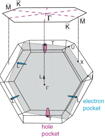
projection on the (1 1 1) surface are shown in figure 2. Close to the T and L points
36
the 6p bands cross the Fermi level, creating hole pockets at the T points and electron
37
pockets at the L points. These pockets are very shallow; the Fermi level is 27.2 meV for
Topological electronic structure and Rashba effect in Bi thin layers 4
Figure 1. Truncated bulk structure of Bi(1 1 1). The solid lines indicate covalent bonds between the atoms within the bilayers. (a) Top view of the first three atomic layers. Each layer consists of a 2D trigonal lattice. Dashed lines indicate the mirror planes of the structure. (b) Side view (projected onto a mirror plane) of the first four layers. Reprinted figure with permission from [12]. Copyright (2005) by the American Physical Society.
the electrons and 10.8 meV for the holes. The bulk Fermi surface elements projected on
1
the surface Brillouin zone are such that the electron pockets and the hole pockets can
2
be found close to the M and Γ points, respectively [2].
3
Interestingly, due to the bulk inversion symmetry, the SOC does not lead to any
4
lifting of the spin degeneracy, on the contrary to the surfaces where this symmetry is
5
broken.
6
Already about 50 years ago, it has been argued [13] that quantum effects could
7
be present on the (1 1 1) surface. This is mainly due to the small effective mass of the
8
electrons (m∗ ≈ 0.003 me) and to their long wavelength at the Fermi level (∼ 12 nm) [2],
9
meaning that defects on the surface are supposed not to play a significant role.
10
Before taking thin films in a review, it is important to take into account changes in
11
the electronic structure at crystallographic surfaces. We will concentrate here only on the
12
(1 1 1) surface because it is the most important for applications: it is the natural cleavage
13
plane and it is the preferred surface resulting from epitaxial growth. For symmetry
14
reasons, this surface gained even more importance with the advent of TIs.
Γ
Figure 2. Bismuth bulk Brillouin zone and its projection on the (1 1 1) surface. The elements of the bulk Fermi surface are shown but not to scale. The pink dashed lines indicate the threefold rotational axis and the three mirror lines of the surface Brillouin zone. Adapted from [2], Copyright (2006), with permission from Elsevier.
2.2. Results from photoemission experiments
1
Pioneering ARPES studies performed on the Bi(1 1 1) face of the bulk crystal were in fair
2
agreement with calculations and shown the presence of surface states in the spin-orbit
3
gaps [14]. Later photoemission measurements, all performed on this surface, refined
4
characterization of the surface states [14–16], revealed a much higher carrier density
5
for the surface and brought the first Fermi surface mapping [17]. It appeared that
6
electronic structure close to the K and Γ points can be interpreted as modified bulk Bi
7
states. An electron pocket was found at the M point, with a higher effective mass than
8
that expected for the bulk states. Near the Γ point, the situation is more complex. More
9
detailed studies indicated that the Fermi surface consists of six elongated hole pockets
10
along the Γ–M directions surrounding a ring-shaped electron pocket centred at Γ, all of
11
which have a 2D character. A weak emission feature associated with the bulk hole pocket
12
in the Fermi surface was as well identified [18, 19]. Further characterization briought
13
better understanding of the surface [20] and bulk bands [21]. Two of the four 2D bands
14
lying close to the Fermi level are part of the complex Fermi surface. The threefold
15
rotational symmetry of these bands indicates a weak interaction with the underlying
16
bulk bands.
Topological electronic structure and Rashba effect in Bi thin layers 6
(a)
(b)
Bi(111)& &hν&=&15&eV&&& k||&(Å/1)&
electronic structure for the three surfaces together with experimental data. In Fig. 2(a) we compare the results for Bi(111) and find excellent agreement for the two split surface states near !". The experimental results also agree with recently published data for Bi(111) [10] but the two split bands appear better resolved here. Here, as in Ref. [10], the intensity of both surface states strongly decreases close to !". This is most likely due to the overlap with the projected bulk band structure. The surface states are no longer genuine surface states but surface reso-nances, which penetrate much more deeply into the crys-tal and give a lower photoemission intensity. Although it is, therefore, not simple to decide if the states are, in fact, degenerate at !" or not, we find no evidence for the latter. This discrepancy with the data of Refs. [10,18] is most likely due to a sample misalignment, which later was found to have been present [11]. Our interpretation is in disagreement with the result from Ast and Ho¨chst, who used a Bi(111) bilayer to simulate the surface-state dis-persion of Bi(111) with a tight-binding model [19]. In their case, the calculated bands match the experimental dispersion beyond the !" point when the bilayer thickness is increased by 70% with respect to the bulk value and when the SOC strength was reduced to 13% of the ex-perimental value 1.5 eV [13]. The bilayer, however, al-ways has inversion symmetry, and therefore this calculation yields two spin-degenerate bands near the Fermi energy that do not cross at !".
Figure 2(b) shows the situation near !" of Bi(110). The experimental results have already been published else-where [7]. In the theory one can clearly see that, as in Bi(111), the surface state on Bi(110) is degenerate at !" and splits into two surface states along the symmetry lines with one electron per k point. In contrast to Bi(111) this surface state is unoccupied at !" and has negative effective electron masses that lead to the formation of the hole FS pocket around !" [7]. This specific behavior of the
surface-state bands is also responsible for the formation of the electron FS pocket between !X1 and !M1 and the hole
pocket at !M1[7]. In the experiment, only the lower branch
of the spin-orbit split state can be observed as it enters the occupied states. Such a situation can be highly confusing, because the band could be mistaken for a simple parabolic hole pocket.
The scenario of a very steep band and a flatter one near !" can also be found on Bi(100). This is shown in Ref. [20] and is therefore not presented here. Instead, Fig. 2(c) shows the situation near the !M0 point. This point is the
!
M point of the quasihexagonal SBZ of Bi(100) which is not lying on the mirror plane of the SBZ (see Ref. [20]). Since all !M points of a (quasi)hexagonal SBZ fulfill the criterion of lying exactly in the middle of the line joining two !" points, we also expect a degenerate surface state here. As Fig. 2(c) shows, this is indeed the case. In fact, here the bands close to the high-symmetry point are so steep that the dispersion cannot be resolved in the experi-ment. In the rest of the SBZ, the agreement between experiment and calculation is more difficult to find. This is due to the deep penetration of the surface states into the bulk, such that even a calculation with a 22 layer film cannot completely avoid the interaction between the two surfaces. Details of the electronic structure of Bi(100) will be published elsewhere [21].
The spin-orbit splitting obtained for the Bi surfaces is a few times bigger than that of the surface state on Au(111) [1,2], which is to be expected since the atomic spin-orbit splitting in Bi is 3 times larger than that in Au. However, the character of the spin-orbit splitting in the present case is different from that in Au(111). For the latter, the electronic structure can be described by a free electron-like two-dimensional surface state at !". In such a case, the spin-orbit interaction can be treated by adding a so-called Rashba term to the nonrelativistic Hamiltonian [22]. This leads to a splitting of the surface state, which
-600 -400 -200 0 200 X1 Γ X'2 0.4 0.3 0.2 0.1 0.0 -0.1 k|| -100 -80 -60 -40 -20 0 20 40 E-E F (meV) M Γ M ( -1) K1 M' K2 -400 -300 -200 -100 0 hν = 16 eV (b) Bi(110) hν = 15 eV (c) Bi(100) hν = 15 eV (a) Bi(111) min max
FIG. 2 (color). Calculated and measured electronic structure in the vicinity of two high symmetry points on three surfaces of Bi. (a) !" on Bi(111), (b) !" on Bi(110), and (c) !M1 on Bi(100). The small black dots are the projected bulk band structure calculated using the tight-binding model of Liu and Allen [17]. The red solid circles are the calculated surface state energies; the thin red line is a guide to the eye. The photoemission intensity is linearly scaled from dark blue (minimum) to white (maximum).
P H Y S I C A L R E V I E W L E T T E R S 23 JULY 2004week ending
VOLUME93, NUMBER4
046403-3 046403-3
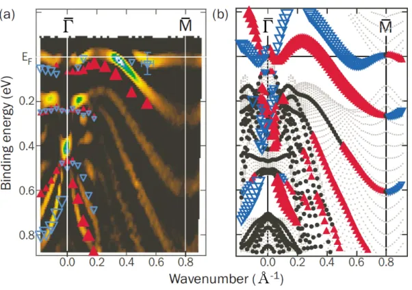
Figure 3. (a) Surface states of Bi(1 1 1) calculated without (black) and with (red) spin-orbit splitting. The shaded areas show the projection of the bulk bands obtained without (violet) and with (yellow) spin-orbit coupling and their superposition (brown). (b) Calculated and measured electronic structure of Bi(1 1 1) along the Γ–M direction. The black dots are the projected bulk band structure calculated using the tight-binding model of Liu and Allen [25]. The red solid circles are the calculated surface state energies; the thin red line is a guide to the eye. The photoemission intensity is linearly scaled from dark blue (minimum) to white (maximum). Reprinted figures with permission from [24]. Copyright (2004) by the American Physical Society.
As Bi is a heavy element, the electronic structure differences between the bulk
1
and the surfaces can be attributed to SOC. The SOC lifts the degeneracy in the bulk
2
electronic structure of solids but this is not the case in solids with inversion symmetry
3
and then the band still contains two possible spin directions. This symmetry is lost at
4
the surface and a kk-dependent splitting of the bands is expected due to the Rashba
5
effect [22, 23]. The first evidence of the influence on the SOC in Bi(1 1 1) was provided
6
by combining experimental data from ARPES with calculations [24] (figure 3).
7
When the SOC term is included in the calculation, it results in a spin splitting of
8
the surface states in all directions, degeneracy remaining only at the Γ and M points
9
[red lines in figure 3(a)]. The strong SOC gives as well a qualitative explanation for
10
the fact that the Bi(1 1 1) surface, which can be viewed as the separation of weakly
11
interacting BLs, is metallic despite of the lack of dangling bonds. On the contrary
12
to the situation at the Γ point where the splitting due to SOC leads to a very steep
13
dispersion of surface states, that at the M point was at the beginning somewhat unclear.
14
Here band degeneracy is expected because M is a high-symmetry point on the surface
15
Brillouin zone boundary. One reason for this difficulty was attributed to the fact that
16
the surface state bands close to the M point are rather surface resonances than genuine
17
surface states.
The ARPES results for Bi(111), shown in figure 3(b), are found to be in good
1
agreement with the calculations for the two split surface states near the Γ point. The
2
intensity of both surface states strongly decreases in the vicinity of this point, most
3
likely due to the overlap with the projected bulk band structure. The surface states
4
are no longer genuine surface states but surface resonances that penetrate much more
5
deeply into the crystal [24].
6
SARPES is the most adapted technique for a deeper insight on the lifting of the
7
band degeneracy and the SP. A strong SP of the photocurrent even from bulk continuum
8
states of Bi(1 1 1) has been observed and shown, on the basis of ab initio one-step
9
photoemission calculations, to originate from the strong SP of the initial states at the
10
surface and to be the result of the surface sensitivity of SARPES. Final state effects
11
cause deviations of the kk dependence of the SP from strictly antisymmetric relative
12
to Γ [26].
13
3. Electronic structure of Bi thin films
14
Today, studies of thin Bi films are still at the centre of a very active research area; so
15
this review can only pretend to give a taste of this rich production. Other recent reviews
16
of theoretical predictions and experimental results obtained by ARPES on Bi surfaces
17
and thin films can be found in references [27–32].
18
3.1. Growth of thin films
19
Bismuth on semiconductor surfaces was extensively studied in the 1990s as a typical
20
ordered metal-semiconductor interface. More recently, in the first decade of the 2000s,
21
the interest in thin films was stimulated by the intriguing physical properties of Bi. These
22
studies necessitated good crystalline quality of the films that was mastered namely on
23
the Si(1 1 1)(7 × 7) substrate [33, 34]. Further on, the quality of the layers was improved
24
by mild annealing [35, 36]. In such a way the thickness of stable hexagonal Bi films
25
could be reduced down to 4 BLs [37]. The Si(1 1 1)(7 × 7) substrate is dominant in the
26
majority of recent reports [33, 35, 38–50].
27
Other semiconductor surfaces are much less used. Similarly to what happens during
28
the growth on Si(1 1 1), the structure of very thin Bi film is unstable on Ge(1 1 1), its
29
orientation changing from (1 1 0) to (1 1 1) at 6–10 BLs [51]. Here, the strong interaction
30
with the substrate leads to the formation of a hexagonal (1 1 1) film; even at 14 BLs, a
31
lattice constant 2% smaller than that of bulk Bi(1 1 1) is observed.
32
The particularity of the III–V semiconductors is to have two different terminations
33
of the (1 1 1) surface. From the initial stages of the Bi deposition the growth on the
34
A face (In-terminated InAs) of the InAs(1 1 1) surface is epitaxial, contrary to that on
35
the B face (As-terminated InAs) that proceeds via the formation of islands. ARPES
36
spectra supported by fully relativistic ab initio one-step photoemission calculations show
37
that the electronic structure of a 10 BL deposit on the A face is identical to that of bulk
Topological electronic structure and Rashba effect in Bi thin layers 8 Bi, while more than ∼ 30 BLs are needed for the B face [52].
1
The surface termination controls as well atom mobility-driven structural changes
2
after Bi deposition and upon subsequent annealing. On the A side, a morphology
3
of circular patterns controlled by Bi atoms mobility is observed. On the B side, no
4
particular morphology is observed due to a stronger chemical interaction between Bi
5
and As atoms [53].
6
Preparation of high quality Bi crystals on other substrates is rather scarce. Quasi
7
layer-by-layer growth mode of Bi nanostructures at low temperature can be realized on
8
highly oriented pyrolytic graphite [54]. Deposition at low temperature, or
surfactant-9
mediated growth, modifies the kinetics of the film growth and enables to get a good film
10
quality even on surfaces of insulators such as α-Al2O3(0 0 0 1) [55]. Metallic surfaces can
11
as well be suitable substrates, as this is the case for Ni(1 1 1) [56], Cu(1 1 1) [57] and
12
Au(1 1 1) [58]. In particular, films above 1 BL on Au(1 1 1) preserve the (1 1 0) symmetry
13
up to ∼ 60 BL. The structural transition from Bi(1 1 0) to Bi(1 1 1) occurs by heating
14
at 470 K. In general, it is difficult to obtain thick Bi(1 1 0) films and thus the Au(1 1 1)
15
substrate is appropriate for investigation of the peculiar electronic characteristics of
16
Bi(1 1 0) [58].
17
3.2. Surface states – Rashba effect
18
The even number of valence electrons makes Bi very close to being an insulator, but
19
the very slight overlap between the conduction and valence bands eventually drives it
20
to a prototype semimetal with a very small number of carriers (3 × 1017cm−3). This
21
leads to an unusually long Fermi wavelength and could open the perspective for the
22
development of devices based on quantum size effects [56, 59]. In this context, it was
23
theoretically proposed that, by making the films thinner, Bi turns from a semimetal
24
into a semiconductor because the related confinement discretizes the perpendicular
25
momentum of the electron and tends to open the gap [60, 61]. In contrast to this
26
scenario, ARPES measurements on ultrathin Bi(1 1 1) films showed surprisingly that the
27
films are highly metallic [38] (figure 4). The long-standing controversy of semimetal to
28
semiconductor transition has finally been resolved. The problem had been controversial
29
because of the subtle fact that the film interior is semiconducting while the surface is
30
always metallic [62].
31
It is clear that the observed metallic surface states are completely different from
32
the projected bulk. The Fermi surface shown in figures 4(a–c) is formed by a hexagonal
33
electron pocket around the Γ point and six hole lobes along the Γ–M direction,
34
schematically shown in figure 4(d), very similar identical to the so-called “crown shape”
35
Fermi surface reported on the cleaved surface [18, 19]. These features do not change
36
with the film thickness.
37
Since the surface states are spin split, the electron and hole doping leads to a
38
switching off of one of the spin channels for surface conductivity, making the doped Bi
39
films potentially interesting for spintronic applications [49]. This can be achieved using
Figure 4. (a–c) The Fermi surface of 6.8, 10 and 17 bilayers (BL) Bi(1 1 1) films, respectively. (d) Schematic drawing of the Fermi surface in the surface Brillouin zone. Electron pockets are coloured in light blue and hole pockets in purple. (e) The band dispersion along the Γ–M direction for the 10 BL film close to the Fermi level. The solid lines through the dots are the results of first-principles calculation with one side of the film terminated with H. The red circles are surface states and the pink ones surface resonances. Reprinted figure with permission from [38]. Copyright (2006) by the American Physical Society.
adsorption of appropriate species. For example upon room temperature adsorption of
1
small amounts of Cs forming a 2D adatom gas, the surface states shift to the higher
2
binding energies by 100–300 meV due to an electronic charge transfer from the Cs
3
adsorbate to the Bi film. As a result, only the electron pockets are left at the Fermi
4
surface. On the contrary, upon adsorption of Sn followed by annealing at 150◦C, Sn
5
atoms dissolve into the Bi film and act as acceptor dopant causing a downward shift by
6
100 meV, only the hole pockets being left at the Fermi surface.
7
Additionally, as already suggested by ab initio calculations for the bulk crystal [24],
8
the surface states show a large Rashba splitting [63], due to the significant SOC [see
9
figures 3(e) and 4(e)].
10
A clear momentum-dependent spin splitting and a SP of the surface state bands
11
has been further observed by SARPES. The spin structure was antisymmetric with
12
respect to the Γ point, as predicted by theory, and the obtained in-plane SP was as high
Topological electronic structure and Rashba effect in Bi thin layers 10
Figure 5. (a) Spin-split band dispersion of a 10 bilayers Bi{1 1 1} film in the Γ–M direction obtained from spin- and angle-resolved photoelectron spectroscopy (triangles) superimposed on non-spin-resolved angle-resolved photoelectron spectroscopy data. (b) The spin-polarized band structure of the ab initio calculations for free-standing Bi slabs. The gray dots represent the bulk band projection. In both panels, the spin-up (-down) channels are shown by red (blue) solid triangles, the size of which indicate the magnitude of the spin polarization. Reprinted figure with permission from [40]. Copyright (2007) by the American Physical Society.
as ±0.5 [40]. However, because of the complex band structure of bulk Bi, the surface
1
state bands do not follow, except for small k-vectors, the behaviour expected from the
2
Rashba picture in which two concentric circles for the Fermi surface are expected [41].
3
The Rashba effect plays the dominant role where the surface states are located
4
in the bulk band gap but changes gradually into a parity effect due to quantum
5
confinement where the surface states start to overlap with the bulk band projection. This
6
demonstrates that band splitting due to different symmetry breaking with completely
7
different characteristics can be smoothly joined and suggests an intriguing crossover
8
between relativistic and quantum size effects. The observed transition is due to a
9
presence of quantum-well states [38–40] that are spin degenerate due to the conservation
10
of the space-inversion symmetry if the whole film is considered. However, the analysis of
11
the charge distribution inside the film and of the in-plane spin component perpendicular
12
to the wave vector reveals a local SP (figure 5) and it was concluded that the spin
13
property at the M point is dominated by the parity effect [41].
So, very early, it appeared that the SP of the Bi surface states cannot be attributed
1
solely to the conventional Rashba splitting as claimed in the first SARPES reports
2
[40, 41]. Improved resolution in SARPES measurements allowed to prove that the
in-3
plane SP is remarkably suppressed on a half of six elongated hole pockets of the surface
4
states and that a giant out-of-plane SP is observed [42, 43]. These unconventional
5
features are explained in terms of symmetry breaking and many-body effects, similarly
6
to the Bi and Pb on Ag(1 1 1) surface alloy systems where the in-plane potential
7
gradient [64] causes the out-of-plane SP [65].
8
For the sake of completeness, let us mention that there is a series of studies dealing
9
with the Rashba effect at the Bi/Ag(1 1 1) interface. Bi is found to induce a giant spin
10
splitting [66] that can be tuned in the surface alloy BixPb1−x/Ag(1 1 1) [67]. It enhances
11
as well the electron-phonon coupling strength which is much stronger than either for
12
the clean Ag(1 1 1) surface state or for bulk Ag [68].
13
Calculations explain the observed large enhancement of the Rashba splitting by
14
the strong distortion of the surface-state wave function which is caused by the surface
15
corrugation [69, 70]. In more detail, the experimentally observed anisotropy of the
16
splitting can only be described if higher-order contributions to the Rashba–Bychkov
17
Hamiltonian are included [71].
18
On decreasing the Bi film thickness, the SP at the M point was found to be gradually
19
reduced as a consequence of the quantum-well states influence (figure 6). It is has been
20
demonstrated that the coupling between the Bi film and the Si(1 1 1) substrate is fairly
21
weak [44], suggesting the nearly free-standing nature of the Bi film. The interface
22
between Bi and Si can be regarded as a “bottom surface” (Si side) where Rashba states
23
similar to those at the normal surface (vacuum side) would emerge due to the breaking
24
of the space-inversion symmetry at the interface. These two Rashba states would have
25
opposite spin directions because of the symmetry requirement. When the Bi film is thick
26
enough, these states are independent from each other. Upon reducing film thickness,
27
the wave functions of the two Rashba states start to overlap and hybridize, eventually
28
leading to a substantially reduced in-plane component of the SP [44, 47].
29
3.3. Spin polarization – Spin-orbital entanglement
30
It seems opportune to remind here that information obtained from photoemission
31
spectra is a function of intrinsic properties of the system under study. As a first
32
approximation, the spin is preserved in the electric dipole transition. So, spin-resolved
33
photoemission can extract the spin character of the electronic states and bring a new
34
information in materials where the band structure is controlled only by exchange
35
interaction. However, for materials where the SOC plays a significant role, as this
36
is the case for Bi, the spin direction may depend on the position both in real space
37
and momentum space, as well as on the symmetry of the states, since the spin is
38
no longer a good quantum number [72, 73]. The experimental geometry, such as the
39
light polarization and the incidence or emission angle, influences the measured SP in
Topological electronic structure and Rashba effect in Bi thin layers 12 (a)
(b)
(c)
Figure 6. (a) Bi thickness dependence of the band dispersion (the second derivative with respect to energy of the energy distribution curves is shown) near the Fermi level (EF) along the M–K direction measured at 30 K on Bi/Si(1 1 1). Energy distribution curves at the M point are also shown for each thickness. (b) Comparison of the thickness dependence of the energy interval (Egap) between the bottom of conduction the band [labelled S3 in (a)] and the top of the quantum-well states (QWS) at the M point with that of the band calculation. (c) Corresponding spin-resolved energy distribution curves (top) and their spin polarization (bottom) in the vicinity of the M point. Reprinted with permission from [44]. Copyright 2012 American Chemical Society.
both magnitude and direction [74]. The SOC mixes states with different spin and
1
orbital character and the light polarization selects the orbital character of the electronic
2
states involved in the photoemission process. So, the spin information obtained from
3
photoemission experiments on spin-orbit influenced surfaces has to be taken with
4
precaution, while it remains reliable for states with pure symmetry [73]. Even if the
5
mirror symmetry governs the spin orientation in the initial states, rotating the
electric-6
field vector of the incident linearly polarized light can break the mirror symmetry of the
7
experimental geometry, which leads to a specific SP of the photoelectrons.
8
The entangled spin-orbital textures have been first explored in TIs [75–78] and later
9
in unoccupied bands of the Bi/Ag(1 1 1) surface alloy [73] and in elemental Bi [50]. Laser
10
excited SARPES studies of the Bi(1 1 1) surface allow to establish a general description
11
of the spin-orbital texture in even-odd parity symmetry. Moreover, a new concept has
12
been developed to determine the phase of the photoemission dipole transition matrix
13
element through the dependent quantum interference, which relies on the
spin-14
orbital-entanglement and the laser field [50].
3.4. Bismuth film as a topological insulator: theoretical approaches
1
TIs are bulk insulators which support protected boundary states [79, 80]. The easiest
2
way to describe a TI is as an insulator that always has a metallic boundary when placed
3
next to a vacuum or an “ordinary” insulator. These metallic boundaries originate from
4
topological invariants, which cannot change as long as the material remains insulating.
5
Nevertheless, these invariants do change in crossing the interface between topological
6
and “ordinary” insulators, so by contradiction the surface cannot remain insulating [81].
7
In two dimensions, this phenomenon is called the quantum spin Hall effect and is
8
distinguished by 1D chiral edge modes propagating along the perimeter of the system
9
that are immune to non-magnetic disorder. It was first theoretically predicted for
10
graphene with spin-orbit interaction included [82] and was further generalized to three
11
dimensions [83–87].
12
Thin films are more relevant to actual device architecture. Efforts have been made
13
to reduce the thickness of known bulk topological insulators [79, 80]. Benefits of a
14
minimal film thickness include: i) bulk conduction and scattering caused by natural
15
defects (a general issue) are minimized; ii) the band gap can be enhanced by quantum
16
size effects; iii) discretization of the bulk bands can turn a semimetal (or a metal) into an
17
insulator. The choice of available materials is thus substantially broadened. However,
18
the usable film thickness has a natural lower limit below which the two film boundaries
19
may be coupled by quantum tunnelling, so that a small, thickness-dependent, gap opens
20
up at the Dirac point, cutting off the spin conduction.
21
The requirement of fine tuning the film thickness makes the experimental fabrication
22
of 2D TIs rather difficult. Therefore, it is desirable to search for simpler materials with
23
strong SOC. Bismuth thin films are candidates of choice. This initiated a large amount
24
of theoretical studies concentrating on the (1 1 1) face [7, 88–107]. Rare are reports
25
on other crystallographic faces. Non-trivial 2D TI phases in 2-BL and 4-BL Bi(1 1 0)
26
have been reported by combining first-principles calculations and scanning tunnelling
27
microscopy [108].
28
Another approach is the searching for new structural phases. Ab initio calculations
29
demonstrate that Bi with the space group No. 139 (I4/mmm) is a topological crystalline
30
insulator. This system takes advantage of dual protection: the Dirac cones are pinned at
31
the high-symmetry points of the (0 0 1) surface; as a consequence they are protected by
32
time-reversal symmetry and, even if in-plane mirror symmetry is broken at the surface,
33
they can survive in the presence of a weak disorder [109].
34
When considering nanostructures, calculations suggest that the topological edge
35
states of zigzag Bi(1 1 1) nanoribbon might be significantly tuned by H edge adsorption,
36
the most remarkable effect being an increase by one order of magnitude of the Fermi
37
velocity as the Dirac point is moved from the Brillouin zone boundary to the Brillouin
38
zone centre, the real-space distribution of Dirac states being twice more delocalized [110].
39
Several band structure calculations based on on a first-principles have been
40
published quite early because an effective single particle picture and the Bloch symmetry
Topological electronic structure and Rashba effect in Bi thin layers 14
Figure 7. (a) Unit cell and lattice vectors, and (b) time-reversal invariant momenta (TRIMs) of a 1 bilayer Bi(1 1 1) film. The TRIMs consist of the Γ point and the three M points. (c) Bulk energy bands and the parity at the TRIMs for a 1 bilayer Bi(1 1 1) film. (d) and (e) Energy bands of the Bi(1 1 1) zigzag- and armchair-edge ribbons, respectively, with a width of 20 unit cells, calculated from the tight-binding model. (f) Energy bands of a eight-unit-cell-wide Bi(111) zigzag-edge ribbon from first-principles calculations. The size of the symbols corresponds to the weight of the states in the edge atoms. Reprinted figure with permission from [91]. Copyright (2011) by the American Physical Society.
still apply. In particular, density functional theory based calculations for Bi(1 1 1)
free-1
standing monolayers and thin films predicted a topological behaviour of such films [90,91]
2
(see e.g. figure 7).
3
The 1 BL Bi(1 1 1) film has a honeycomb structure, if one neglects the out-of-plane
4
coordinate. Therefore, as in graphene, it is possible to refer to the two types of simple
5
edge shapes as zigzag and armchair edges. Figures 7(d) and 7(e) show the energy bands
6
of zigzag- and armchair-edge ribbons of the Bi(1 1 1) BL calculated in the tight-binding
7
framework. In both figures, the number of Kramers pairs of edge states per one edge
8
is odd, confirming that the 1 BL Bi(1 1 1) film is a quantum spin Hall system. Result
9
from the tight-binding model [figure 7(d)] and that from a first-principles calculation
10
[figure 7(f)] are in good agreement [91].
11
Further theoretical study [90] indicated a more complex behaviour of the Bi(1 1 1)
12
films. The film below 4 BLs is an intrinsic 2D TI with a band structure consisting of
13
“molecular orbital” levels without distinction between surface bands and bulk bands.
14
Above 4 BLs, the band structure is made of surface bands superimposed onto 2D
15
projected bulk bands. The projected 2D bulk bands still keep the non-trivial topology
16
of a 2D TI with a sizeable gap, but the surface bands gradually appear in the middle of
the projected bulk band gap with increasing film thickness (see also [89]), leading to a
1
semiconductor (1–4 BLs) to a semimetal (5–8 BLs) transition. It is proposed that the
2
trivial metallic surface states can be removed by surface H adsorption which effectively
3
converts the Bi films into true 2D TIs [89].
4
As it is demonstrated in this review, the SARPES plays a central role for the
5
investigation of TIs and the closely related Rashba-type systems. Various experimental
6
aspects of the spin polarised photoemission have been reviewed and discussed by
7
Dil et al. [111]. The first-principles studies beyond the ground state, i.e. addressing
8
spectroscopic properties and perhaps possible disorder/interdiffusion scenarios, are rare.
9
The interpretation of the corresponding spectra is in general based only on the calculated
10
bands [112] or Bloch spectral functions [64], respectively. So far, simplifying models have
11
been used to discuss for example the origin of the SP monitored by SARPES [113]. The
12
role of the divergence of the radiation vector potential at the surface and the possible
13
connection between circular dichroism in ARPES and the SP have been investigated only
14
recently for the Bi/Ag(1 1 1) Rashba system using a tight-binding model [114]. In spite of
15
the considerable success of SARPES, the reliability of this method for the investigation
16
of the spin properties of TI surfaces has been discussed in various experimental [115,116]
17
and theoretical [113, 117] studies. Part of these works involves the interpretation of the
18
circular dichroism in the ARPES as the SP of Rashba split and topological surface
19
states [115–117]. If this would be correct it can improve the efficiency of SP detection.
20
Recent experimental and theoretical studies [118, 119] clarified that measuring circular
21
dichroism cannot replace the more demanding spin-resolved measurements which also
22
calls the recent theoretical conclusions [114,120] into question. Generally speaking,
spin-23
resolved photoemission does not allow directly identifying the measured SP to the initial
24
states SP. The photoemission excitation process related aspects of measured SP have to
25
be addressed within an ab initio study based on the one-step model of photoemission
26
which accounts for all relativistic effects, the surface geometry as well as all matrix
27
element effects at the same level [121,122]. In particular most of the theoretical analysis
28
are based on very simplified approximations, e.g. free electron final state and normal
29
emission geometry. This leads to various interpretations of the measured SP which
30
might be misleading. The very few one-step model investigations on TIs together with
31
the experiments on Rashba systems [73,123] clearly demonstrate the need for the support
32
of theoretical investigations to deduce unambiguous information from experimental
33
SARPES data. This holds in particular when the photon energy is varied over a wide
34
range to change the probing depth [124, 125].
35
3.5. Bismuth thin layers on topological insulators
36
All mentioned theoretical works clearly suggested topological properties of Bi to be
37
reduced to one or several BLs. However experimentalists faced difficulties to verify it.
38
No topological effects were reported experimentally on deposited BLs of Bi, probably
39
because of its unique surface and interface properties [2]. As already mentioned, the
Topological electronic structure and Rashba effect in Bi thin layers 16
Figure 8. (a) Angle-resolved photoelectron spectroscopy (ARPES) image along the Γ–M direction of a 5 bilayers (BL) Bi(1 1 1) film on Bi2Te3 (raw data) and (b) its second derivative with respect to energy. (c) The calculated weighed spectral function (WSF) for a 5 BL strained Bi(1 1 1) film, which is the band dispersion weighed by the magnitude of the wave function localization at the topmost Bi BL. (d) Experimentally measured raw ARPES image and (e) its second derivative with respect to energy along the Γ–M direction of the 6 BL Bi(1 1 1) film on Bi2Te3. (f–g) The WSF for a 6 BL strained Bi(1 1 1) film [in (f) the optimized structure in the calculation is used, whereas in (g) the experimentally obtained lattice parameters are used; the arrows show the slight energy change]. (h) The WSF for a 7 BL strained Bi(1 1 1) film. (i) The band dispersion for the 7 BL strained Bi(1 1 1) film together with the bulk band projection (the size of the circles indicates the magnitude of the surface localization of the wave function; SS and QWS represent surface and quantum-well states, respectively). Reprinted figure with permission from [126]. Copyright (2012) by the American Physical Society.
initial growth of Bi on non lattice-matching substrates, namely on Si(111), typically
1
resulted in a pseudocubic Bi(1 1 0) BL. Only upon additional deposition, Bi(1 1 1) begins
2
to form, the film being presumably too thick to maintain the predicted states.
3
In order to circumvent the difficulties of preparing a single Bi BL on commonly
4
used substrates, as Si(1 1 1), the straightforward idea is to realize the deposition directly
5
on existing Bi-based TIs. Using such an approach problems connected with epitaxial
6
growth can be solved in a simple way. Subsequently, the atomic and electronic structures
7
of Bi(1 1 1) films grown on Bi2Te3, Bi2Se3, Bi2Te2Se and Bi2Te2.4Se0.6 [76, 126–132] have
8
been determined by means of several techniques, namely ARPES, and compared to
9
first-principles calculations. Some of the results have been reviewed in [27].
10
ARPES studies using TIs as a substrate do not allow however to form a conclusive
11
assessment because the similarities in the electronic structures of the Bi film and of the
12
substrate preclude disentangling their respective contributions to the data.
One of the driving forces of the topological transition is the strain due to the
1
lattice mismatch. For instance, when the Bi(1 1 1) film is grown on Bi2Te3(1 1 1),
2
it is horizontally contracted and vertically expanded compared to the bulk values.
3
ARPES studies show that this lattice distortion induces a change in the surface state
4
band dispersion and the theoretical calculation reveals that 3D Bi becomes topological
5
(figure 8). This can be recognized in edge state dispersion [see figure 8(i)] [126]. While
6
one of the surface states connects to the valence bands at both the Γ point and the M
7
point, the other one connects to the valence band at the Γ point and the conduction
8
band at the M point, a characteristic feature of topological edge states.
9
When measuring the spin texture, this one is the same for the intrinsic Dirac
10
cone of Bi2Se3 or Bi2Te3 surface states, the extrinsic Dirac cone of Bi BL induced by
11
the Rashba effect and the hybridized Dirac cone between the former two states [76].
12
However, according to [130], the strong hybridization between Bi and the Dirac-cone
13
states in Bi2Te3 observed in 1 BL film does not occur for other thicknesses. On the
14
contrary, in another study [131], a direct experimental signature has been found that
15
even a thicker film, 30 nm Bi(1 1 1)/Bi2Te3, can be topologically non-trivial in three
16
dimension. At the same time the authors concede that the origin of these non-trivial
17
properties is not yet understood and needs further investigations.
18
Slightly more convincing confirmation is brought up using real-space resolution of
19
scanning tunnelling microscopy and spectroscopy (STM/STS). The edge states can be
20
directly observed on single BL Bi(1 1 1) islands, in both real and energy spaces, which
21
are grown on clean Bi2Te3 and Bi(1 1 1)-covered Bi2Te3 substrates [128].
22
A similar STM study on a well-ordered single Bi BL with zigzag edges, grown
23
epitaxially on a cleaved Bi2Te2Se crystal represents a clear real space observation of the
24
edge electronic states of a 2D TI, correspondin,g to a quantum spin Hall state [129]. It is
25
shown that the strong interfacial interaction with the substrate induces a large splitting
26
of the degenerate valence bands of Bi(1 1 1) and the band hybridization with those of the
27
substrate. The hybridization leads to the formation of a characteristic interfacial state
28
and a small hybridization energy gap above the Fermi level for the Bi film. Irrespective
29
of such a strong interaction with the substrate, the band inversion of the Bi film and
30
the edge state are shown to be robust. The edge state along the zigzag edge exhibits
31
a substantial energy shift. This edge state signature was unambiguously resolved in
32
the STS spectra and spatial maps [129] (figure 9). But, according to the authors, the
33
topological or helical nature of the edge state has to be confirmed further, for example,
34
by a spin-polarized tunnelling experiment.
35
3.6. Bismuth thin layers: edge states
36
Another approach in the quest of topological properties of Bi films is to continue
37
auscultating the edge states on substrates that are not TIs; for instance, looking
38
at terraces on top of a Bi monocrystal [48, 133–136]. As indicated by theoretical
39
considerations some years ago, a 3D Bi crystal is topologically trivial [137] whereas a
Topological electronic structure and Rashba effect in Bi thin layers 18
Figure 9. Two-dimensional plot of the scanning tunnelling spectroscopy (STS) ( dI/ dV ) line scan along the arrow indicated in the inset, that crosses one zigzag edge of a Bi(1 1 1) bilayer island. The topography image in the inset covers a 20 × 20 nm2area. Three major spectral features of the Bi(1 1 1) bilayer film and the distinct edge state are indicated by arrows. The topographic profile obtained during the STS measurement is given at the bottom of the figure. Reprinted figure with permission from [129], where further details can be found. Copyright (2014) by the American Physical Society.
non-trivial Z2 topology of Bi(1 1 1) thin films can persist even in the case of multi-bilayer
1
thick films [90]. The thickness limit where topological properties vanish is not clearly
2
predicted by theory and up to date reported experimental results are contradictory.
3
The question arises whether terraces present on the surface and/or vicinal surfaces
4
could harbour a quantum spin Hall effect. The first indication in this direction was
5
discovered on the (1 1 4) surface of a Bi bulk crystal which was found to support a
6
quasi 1D, metallic surface state. The electronic structure at the Fermi level consists of
7
only two crossings with opposite spin and k, and therefore strongly resembles the edge
8
states in the quantum spin Hall effect [133].
9
STM based mechanical and electrical characterization techniques, bring as well
10
evidence of the quantum spin Hall phase in a two-dimensional crystal produced the
11
mechanical exfoliation of a Bi(1 1 1) BL [138]. Electrical conductance measurements of
12
Bi nanocontacts created by repeated tip-surface indentation at temperatures of 4 K and
13
300 K testify the presence of plateaus of conductance G0 = 2e2/h at room temperature.
14
Similarly, later theoretical study claimed that all of the predicted topological
15
properties of the edge states of a free-standing Bi BL will be present even on top of
16
a cleaved Bi(1 1 1) bulk crystal which was confirmed by STM experiments [134]. At the
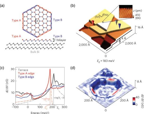
(d) (c)
(b) (a)
Figure 10. Edges of Bi bilayer islands on a Bi crystal surface. (a): Schematics of the Bi bilayer atomic structure (upper panel: top view; lower panel: side view). Type A and type B edges, i.e. edges terminated by atoms close to the vacuum and to the substrate underneath, are shown by the red and blue lines, respectively. The Bi lattice constant is 4.5 ˚A. (b) Topographic image of the Bi(1 1 1) single-crystal surface. The height of the Bi bilayer islands is 4.0 ˚A (line profile on the right). The inset shows a 30 × 30 ˚A2 atomically resolved topographic image of a zigzag edge. (c) Point spectroscopy at the two different types of edge A (red line) and B (blue line) and on the surface away from the edges (grey line). Whereas the spectrum on the type A edges shows a maximum at E2= 183 meV that can be fitted to the expected 1D density of states (dashed orange line), the spectrum on the type B edge is almost featureless. (d) Topography close to the hexagonal diatomic depression, false-coloured with differential conductance at E2= 183 meV. A high conductance (in red) is observed at every other edge of a hexagonal pit-like defect. Reprinted by permission from Springer Nature: Nature Physics (reference [134]), Copyright (2014).
same time the authors of reference [134] point out that the presence of such topological
1
1D edge states (see figure 10) of the Bi BL does not imply that the bulk Bi crystal
2
is topologically non-trivial. Similar findings were supported by a more recent work on
3
thick Bi(1 1 1) films grown on a Si substrate [135].
4
On the other hand, Bi thin films on Si(1 1 1) fabricated with many edge structures
5
exhibit 1D states with a giant Rashba effect and a sizeable out-of-plane SP but are
6
found to have a topologically trivial nature [48]. These findings are supported by a
Topological electronic structure and Rashba effect in Bi thin layers 20
Figure 11. (a) Band structure of the free-standing Bi thin film in planar honeycomb structure ith a lattice constant at 5.35 ˚A. (b) Atomic structure of Bi honeycomb on a SiC(0001)-(√3×√3) substrate. (c) Band structure of the Bi honeycomb on SiC(0 0 0 1)-(√3 ×√3). Red crosses and blue circles identify Bi-derived states with opposite spins. (d) Blow-up of the band structure of (c) around the K point. Red and blue colours refer to opposite spin polarizations of the bands. Reprinted figure with permission from [93]. Copyright (2013) by the American Physical Society.
later calculations [136] where the 1D band structure of step edges of Bi(1 1 1) films
1
was explicitly studied as a function of the film thickness. It unambiguously appeared
2
that the dispersion of step-edge states reflects the topological nature of the underlying
3
films, rather than indicating the existence of topological edge states along step edges
4
on surfaces of a bulk Bi(1 1 1) crystal or a sufficiently thick Bi(1 1 1) film. The trivial
5
step-edge states have the spin splitting of 1D Rashba bands.
6
Looking at all these aforementioned results, it appears that the true nature of the
7
edge states is still waiting to be elucidated in more detail.
8
3.7. Bismuthene: the ultimate layer
9
Following the prediction of topological properties for a free-standing single BL of
10
Bi [7, 91] many theoretical studies proposed suitable substrates allowing building real
11
films with a stable structure [93, 95, 97–100, 102, 103, 105].
12
At this stage, it is useful noting that the terminology in literature slightly evolved
13
and in analogy with graphene the names of single-layered materials are often extended
14
with suffix “-ene” [96]. So, here, we will speak about bismuthene and, similarly to
15
hydrogenated graphene or graphane, we may refer to hydrogen terminated bismuthene
16
as bismuthane [100]. In the same logic, the porous allotrope of a Bi monolayer is
17
denominated as bismuthylene [105]. Electronic structure of free-standing bismuthene
(a) (b) (c)
(d) (e)
Figure 12. Bismuthene on SiC(0 0 0 1) structural model. (a) Sketch of a bismuthene layer placed on the threefold-symmetric SiC(0 0 0 1) substrate in a (√3 ×√3)R30◦ superstructure. (b) Topographic scanning tunnelling microscopy (STM) map showing that bismuthene fully covers the substrate (the flakes are of ∼ 25 nm extent, limited by domain boundaries). (c) Substrate step height profile, taken along the red line in (b), corresponding to SiC steps. (d) The honeycomb pattern as seen on smaller scan frames. (e) Close-up STM images for occupied and empty states (left and right panel, respectively) that confirm the formation of Bi honeycombs. Reprinted with permission from [140]. Copyright 2017 American Association for the Advancement of Science.
has been addressed in [101, 104] and that of double layer bismuthene in [106]. Some
1
aspects of single-layer films of the group V elements, the so-called pnictogens, have
2
been reviewed in [139].
3
Theoretical studies show that the Bi(1 1 1) film on a suitable substrate represents
4
an interesting case with an intermediate inter-bilayer coupling strength and where the
5
strain induced by a substrate can as well induce topological properties [93]. The authors
6
define here a measure of band inversion strength which provides a basis for constructing
7
a topological phase diagram of Bi BLs for assessing the robustness of the non-trivial
8
topological phases as a function of strain and/or the size of buckling. The analysis
9
indicates that insulating and weakly interacting substrate hexagonal-BN could be a
10
good substrate candidate for a nearly free-standing 2D quantum spin Hall phase of the
11
Bi BL film.
12
Turning to larger strains or lattice constants where the Bi BL assumes the planar
13
honeycomb structure, the candidate substrate for support is SiC(0 0 0 1)-(√3 ×√3) with
14
the Bi lattice constant of 5.35 ˚A (figure 11). The substrate induces pronounced
spin-15
splitting of bands around the K point [figure 11(d)]. This planar Bi honeycomb has
Topological electronic structure and Rashba effect in Bi thin layers 22 been previously thought to be a trivial insulator [93]. However, in a later study by the
1
same authors [100], it has been reevaluated and finally shown that the substrate forces
2
this trivial film into becoming non-trivial. The underlying physical mechanism is due
3
to an orbital filtering effect of the substrate [98].
4
Following this prediction, it was possible to grow the first Bi BL on a SiC(0 0 0 1)
5
substrate [140]. This substrate is not only stabilizing the quasi-2D TI but also plays
6
a pivotal role for achieving the large gap, with the strong on-site SOC coming directly
7
into play. The observed structure has a (√3 ×√3)R30◦ superstructure of Bi atoms in
8
honeycomb geometry. The resulting lattice constant of 5.35 ˚A is significantly larger than
9
that of buckled Bi(1 1 1) BLs. This induces a fully planar configuration of the honeycomb
10
layer. Although the topological character of the edge states has experimentally yet to be
11
established, i.e. by a direct transport measurement of the quantum spin Hall effect with
12
its universal quantized conductance, the agreement between experimental evidence and
13
theoretical prediction already strongly suggests that the quantum spin Hall scenario in
14
Bi/SiC is valid.
15
3.8. Possible future prospects
16
As mentioned in section 3.4, checking theoretical predictions concerning thin film
17
topological phases is often a challenge hard to overcome experimentally. We saw for
18
instance that this is the case of the ultimate Bi layer (section 3.7). Another example is
19
a new structural phase of Bi-139(001) (see section 3.4) that is a topological crystalline
20
insulator taking advantage of dual protection [109].
21
The main origin of the difficulty to fabricate such systems lies in the limitation of
22
the available growth techniques.
23
Embedding Bi atoms in an appropriate structure appears to be one of possible
24
approaches to circumvent these difficulties, as it has been shown for the InBi crystal.
25
A thorough analysis combining ARPES measurements and fully-relativistic ab initio
26
electronic band calculations of InBi(0 0 1), grown on the InAs(1 1 1)-A surface, indicates
27
that the topmost Bi BL has the same structure as Bi in the space group No. 139
28
configuration [141]. Nonetheless, the mirror plane parallel to the (0 0 1) plane for Bi-139
29
does not exist within InBi, which indicates that only a single BL of Bi-139 has been
30
created. However, the general surface symmetries of the systems are the same: both
31
ΓM and ΓX are mirror planes for both InBi(0 0 1) and Bi-139(0 0 1). Consequently,
32
the topological states are protected by both, by time-reversal and discrete rotational
33
symmetry [142].
34
The InBi crystal structure in the [0 0 1] direction can be seen as a stacking of [Bi–
35
(2 In)–Bi] trilayers, with a Bi excess layer on the top of the surface [see figure 13(b)].
36
Bloch spectral function depicting the general band dispersion around the M point, where
37
the Dirac point is located, is shown in figure 13(c). The surface topological states
38
are originating from the pz orbitals of the excess Bi atomic layer and they resonantly
39
propagate via the bottom Bi atoms of the trilayers down to the bulk. This is shown in
a b c Bi In a b c Bi excess layer tr ilay er tr ilay er Re lati ve in te ns ity 1 0.5 0 trilayer trilayer Bi excess layer 1.0 0.5 0.0 Re la ti ve In te ns it y (a .u .) Bi In
(a)
1600 1500 1400 1300 1200 1100 1000 900 800 700 600 500 400 300 200 0 -0.2 -0.4 k (Å-1) 0.2 M X Γ 0.5 -0.5 0 Bi nd in g en ergy (e V) 1.0(c)
(d)
(b)
min max surface bulk 1600 1500 1400 1300 1200 1100 1000 900 800 700 600 500 400 300 200 100Figure 13. (a) Top- and (b) side-view of the InBi crystal in the [0 0 1] direction. The crystal can be seen as a stack of Bi–In–Bi trilayers terminated by an excess Bi layer on the surface. (c) Bloch spectral function depicting (in logarithmic colour scale) the general band dispersion around the M point, where the Dirac point is situated. (d) Normalized intensities taken at the Dirac point and plotted from the excess layer towards the bulk of the crystal. For clarity, the intensities of both In atoms in the indium layer are shown. From [141].
figure 13(d), where the normalized intensities are taken at the Dirac point and plotted
1
from the excess layer towards the bulk of the crystal.
2
This experimental realization of a theoretically predicted Bi topological crystalline
3
insulator with outstanding properties opens the gate for future developments in the
4
band-gap engineering of devices.
5
4. Summary
6
Topologically ordered phases of matter have recently received considerable attention
7
both for their intrinsic physical interest and for the paths they may open towards
8
technological breakthroughs. A great deal of attention has been placed on Bi-based
9
systems because of the strong spin-orbit coupling of this heavy element, which could
10
lead to get a large Rashba spin splitting. This, in combination with topological surface
11
states, might lead to new developments in spintronics. In this contribution, an attempt
12
has been made to summarize the present status of the research in this field as well as to
13
present some ongoing research advances. It is underlined that, despite the availability of
14
many theoretical predictions for topological phases in thin films, elaborating these films
15
“in real life” is far from easy. Nevertheless, in the light of the progress already made,