HAL Id: hal-02470287
https://hal.univ-lorraine.fr/hal-02470287
Submitted on 7 Feb 2020
HAL is a multi-disciplinary open access
archive for the deposit and dissemination of
sci-entific research documents, whether they are
pub-lished or not. The documents may come from
teaching and research institutions in France or
abroad, or from public or private research centers.
L’archive ouverte pluridisciplinaire HAL, est
destinée au dépôt et à la diffusion de documents
scientifiques de niveau recherche, publiés ou non,
émanant des établissements d’enseignement et de
recherche français ou étrangers, des laboratoires
publics ou privés.
On the origin of the sharp, low-field pinning force peaks
in MgB2 superconductors
Michael Koblischka, Alex Wiederhold, Anjela Koblischka-Veneva, Crosby
Chang, Kévin Berger, Quentin Nouailhetas, Bruno Douine, Masato Murakami
To cite this version:
Michael Koblischka, Alex Wiederhold, Anjela Koblischka-Veneva, Crosby Chang, Kévin Berger, et al..
On the origin of the sharp, low-field pinning force peaks in MgB2 superconductors. AIP Advances,
American Institute of Physics- AIP Publishing LLC, 2020, 10, pp.015035. �10.1063/1.5133765�.
�hal-02470287�
force peaks in MgB
2
superconductors
Cite as: AIP Advances 10, 015035 (2020); https://doi.org/10.1063/1.5133765
Submitted: 26 October 2019 . Accepted: 14 December 2019 . Published Online: 16 January 2020 Michael R. Koblischka , Alex Wiederhold, Anjela Koblischka-Veneva, Crosby Chang, Kévin Berger , Quentin Nouailhetas , Bruno Douine, and Masato Murakami
ARTICLES YOU MAY BE INTERESTED IN
Atomic structures and nanoscale electronic states on the surface of MgB2 superconductor
observed by scanning tunneling microscopy and spectroscopy
AIP Advances
ARTICLE scitation.org/journal/advOn the origin of the sharp, low-field pinning
force peaks in MgB
2
superconductors
Cite as: AIP Advances 10, 015035 (2020);doi: 10.1063/1.5133765 Submitted: 26 October 2019 • Accepted: 14 December 2019 • Published Online: 16 January 2020
Michael R. Koblischka,1,2,a) Alex Wiederhold,1 Anjela Koblischka-Veneva,1,2 Crosby Chang,3 Kévin Berger,4
Quentin Nouailhetas,1,4 Bruno Douine,4 and Masato Murakami2
AFFILIATIONS
1Institute of Experimental Physics, Saarland University, Campus C 6 3, 66123 Saarbrücken, Germany
2Superconducting Materials Laboratory, Department of Materials Science and Engineering, Shibaura Institute of Technology, 3-7-5 Toyosu, Koto-ku, Tokyo 135-8548, Japan
3Institut Jean Lamour, UMR CNRS-Université de Lorraine, 54506 Vandœvre-lès-Nancy, France
4Groupe de Recherche en Energie Electrique de Nancy (GREEN), Université de Lorraine, 54506 Vandœvre-lès-Nancy, France
a)Author to whom correspondence should be addressed:m.koblischka@gmail.comandmiko@shibaura-it.ac.jp
ABSTRACT
Various MgB2thin films and single crystals were found in the literature to exhibit a sharp, narrow peak at low fields in the volume pinning
force,Fp(H)-diagrams. The origin of this peak is associated with a steep drop of the current density when applying external magnetic fields
and is ascribed to sample purity. We show here that bulk MgB2prepared by spark-plasma sintering also shows the sharp, narrow peak inFp.
The peak is also seen in the volume pinning force scaling,Fp/Fp,maxvsh = H/Hirr. Furthermore, polycrystalline bulk MgB2samples prepared
close to the optimum reaction temperature reveal this peak effect as well, but other samples of the series show a regular scaling behavior. The combination of magnetization data with data from electric transport measurements on the same samples demonstrates the origin of this peak effect. On increasing preparation temperature, the pinning force scaling changes from grain boundary pinning to point pinning and the grain connectivity gets worse. Hence, the sharp, low-field peak inFpvanishes. Therefore, the occurrence of the peak effect inFpgives important
information on the grain coupling in the MgB2samples.
© 2020 Author(s). All article content, except where otherwise noted, is licensed under a Creative Commons Attribution (CC BY) license (http://creativecommons.org/licenses/by/4.0/).https://doi.org/10.1063/1.5133765., s
I. INTRODUCTION
The metallic superconductor with the highest transition tem-perature, MgB2, is considered as a candidate material for many
applications such as trapped field magnets, tapes, and wires due to its simplicity and the simple preparation route possible, even though itsTcis much lower than most of the high-Tc
supercon-ductors.1,2 Even in sintered, polycrystalline MgB2samples, it was
found to be possible to establish a current flow through the entire sample perimeter as the grain boundaries (GBs) do not act as weak links, but as flux pinning sites, e.g., in Nb3Sn.3,4Together with
mod-ern cryocooling techniques, the lowerTc does not pose a serious
problem.5On the other hand, MgB2has its own characteristic
mag-netic behavior including dendrite-like flux penetration,6flux jump effects,7and peculiar flux pinning properties,8which may influence
possible applications. Therefore, these points must be understood properly.
For the flux pinning behavior, the analysis of the flux pinning forcesFp=jc×B (where jcdenotes the critical current density, and
B = μ0H) using the scaling approach by Dew-Hughes (DH)9 and
Kramer10is an important issue. The flux pinning in MgB2is mainly
provided by GB-pinning and point-pinning. Two peculiar observa-tions of the flux pinning analysis on MgB2include (i) the change
of the main acting pinning mechanism with increasing tempera-ture found in polycrystalline samples prepared with varying reaction temperatures11and (ii) the appearance of a sharp, narrow peak in the Fp−H diagrams at relatively low applied fields.12–21Such a peak was observed first in MgB2single crystals22,23and then in thin films.24–26
The occurrence of this peak at relatively low fields was ascribed to the strong decrease injc(B) due to sample purity.
AIP Advances 10, 015035 (2020); doi: 10.1063/1.5133765 10, 015035-1
In this contribution, we analyze magnetization data obtained on a spark-plasma sintered (SPS) MgB2sample with a highly dense
microstructure27and compare the results with a series of sintered, polycrystalline bulk MgB2samples prepared with varying reaction
temperatures.28On all samples, we have performed electric trans-port measurements,31,32 the behavior of which enable us now to clarify the origin of the peak found in theFp-diagrams.
II. EXPERIMENTAL PROCEDURE
The MgB2sample was prepared by SPS at 1200○C and a
uniax-ial pressure of 50 MPa. The sample reached a density of 2.61 g/cm3 (99.2%).27Our data are compared to sintered, polycrystalline MgB2
samples fabricated in the solid state reaction in a pure Ar atmosphere with reaction temperatures between 750○C and 950○C.28For
super-conducting quantum interference device (SQUID) measurements, small samples (2 mm × 2 mm × 1.5 mm) were cut from the big pel-lets. For the resistance measurements, small bars (10 mm × 1 mm ×1 mm) were prepared and the contacts were fixed with silver paint, ensuring a 5 mm distance between the voltage pads. The magnetic characterization measurements were performed using SQUID mag-netometry (Quantum Design MPMS3), and the magneto-resistance characteristics were recorded using an Oxford Instruments 8 T Tes-latron system. The critical current densities were calculated from the magnetization loops using the extended Bean model for rectangular samples.29 Electron backscatter diffraction (EBSD) and transmis-sion electron microcopy (TEM) were performed on TEM-slices pre-pared using focused ion-beam milling. Details of these procedures are given in Ref.30and thesupplementary material.
III. RESULTS AND DISCUSSION
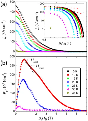
Figures 1(a)and1(b)presentjcas a function of the applied
field, μ0Ha(a), and the volume pinning force,Fp, as a function of
the field (b) of the SPS sample at various temperatures. In (b), the definitions ofHpeakdenoting the position of the sharpFppeak and
Hcrossmarking the crossover field after the peak are given. The peak
and shoulder shape of theFp(H) curves is observable up to 30 K. The
inset toFig. 1(a)gives thejc(H, T) data in a double-log plot. Here,
two regions are clearly distinguishable, as indicated by the dashed lines. The flat region at low fields can be considered to be the single-vortex pinning region, whereas the connected sloped region is where weak collective pinning is dominant.33–35The values of the exponent
β in jc(H) ∝ H−β in the sloped region are around 1.0 at 5–25 K,
1.15 at 30 K, and 1.2 at 35 K, indicating that the decreasing slope of jc(H) gradually becomes steeper at temperatures above 25 K due to
thermal fluctuation effects.36,37
Figure 2(a)–2(d) show the peak region of the Fp vs μ0Ha
-diagrams for samples SPS (a), S775 (b), S850 (c), and S950 (d). The signature of the sharpFp-peak is clearly visible in (a) and (b),
whereas only traces are seen in (c), and in (d), theFp−H behav-ior is fully regular. The pinning force scaling analysis is based on the approach of DH.9The scaled pinning force dataf = Fp/Fp,max
vs h = Ha/Hirr can be fitted to the functional dependence given
byf = A ⋅ (h)p⋅(1 −h)q, withA being a numerical parameter, and p and q are describing the actual pinning mechanism. The posi-tion of the maximum in theFpplot,h0, is given byp/(p + q). For
MgB2, the pinning at GBs (p = 0.5 and q = 2) and the pinning at
FIG. 1. Data of the MgB2SPS sample. (a) jcas a function of the applied field,
μ0Hext, in the temperature range 5 K ≤ T ≤ 35 K. The inset shows the same data in a double-log plot, together with the linear behavior as indicated by the dashed lines. (b) Pinning force, Fp, as a function of the applied field,μ0Hext, calculated from the jc(Ha)-data for T = 10 K, 20 K, and 30 K. At the 10 K curve, the peak position, Hpeak, and the crossover field, Hcross, are indicated by arrows.
non-superconducting point pins (p = 1, q = 2) are the most impor-tant functions.Figure 2(e)gives the DH-scaling of the SPS sample. The pinning force scaling is well developed, and the fit (red line) to all data yields a peak positionh0= 0.21, which clearly points to a
dominant flux pinning provided by extended defects, i.e., GBs. The pinning force scaling of all samples studied is given inFig. S1of the supplementary material.
Now, we turn to the origin of the peak effect in theFp
(H)-curves. From the literature, we can extract the following findings concerning the sharp, narrow peak inFp(H):
(i) Single-crystals and high-quality thin films exhibit the specific Fp-curve shape.
(ii) Sintered, polycrystalline samples, normal thin films, and powders do not show any peculiarFp-curve shape.
(iii) The peak shows a clear temperature dependence; therefore, matching effects are excluded.
(iv) The peak is located at relatively high fields, which implies that surface effects are excluded.
AIP Advances
ARTICLE scitation.org/journal/advFIG. 2. [(a)–(d)] Pinning forces vs applied field for samples: (a) SPS, (b) S775, (c) S850, and (d) S950. (e) Pinning force scaling, f vs h of the SPS sample.
The peak positions, Hp, and the respective crossover fields,
Hcross were extracted from the Fp-data.Table I gives the data of
all bulk MgB2samples and those of Ref.26for comparison. The
smaller values of Ref.26demonstrate the demagnetization effects. The values ofHpare sufficiently large to be above the full penetration
field.
TABLE I. Values for Hpand Hcrossfor all MgB2bulk samples studied here and those of Ref.26(MgB2thin film, 700 nm thickness), together with data forΔρ and the connectivity, K. The scaling parameters A, p, and q are found inTable S1of the supplementary material. All magnetic data are for T = 10 K. For details of the electric measurements, see Ref.32. The ∗ indicates that these values are for the normal peak in Fp, not the sharp peak as in the case of the other samples. Correspondingly,
there is no value for Hcross. n.a. indicates that there are no data available. Sample name Treaction(○C) Hp(mT) Hcross(mT) Δρ (μΩ cm) K (%) S775 643 907 140 4.51 S800 826 1305 77 8.195 S805 798 1525 37 17.054 S850 802∗ . . . 64 9.859 S950 897∗ . . . 113 5.584 SPS 883 1447 6.5 97.076
Reference26 54 122 n.a. n.a.
Figure 3presents the temperature dependence of the extracted critical fields.HpeakandHcrossare well belowHirr. The values ofHpeak
clearly show a sample size dependence as the values here are much larger as compared to the thin-film data of Ref.26; thus, demagneti-zation effects play a role. Here, it should be noted that our values ofHpeakare outside the range of present-day magneto-optics,38,39
and so no direct observations of the flux patterns aroundHpeakare
possible.
The first finding of the present work is that sintered, polycrys-talline samples prepared at reaction temperatures close to the opti-mum value (i.e., ∼800○
C28) do show the sharpFp-peak, whereas all
other samples prepared at higherT do not. The SPS sample with its high density also exhibits the sharpFp-peak.
The electric transport measurements elucidate the grain con-nectivity K, which plays an important role for the current flow through the sample (seeTable I).K is calculated from the resistance data obtained viaK = Δρg/Δρ, with Δρg= 6.31 μΩ cm for randomly
oriented 3D samples, and Δρ = ρ(300 K) − ρ(40 K).40In our series of samples,K was found to increase steeply with increasing reaction temperature from 775○C to 805○C and then decreases again when
increasing the temperature up to 950○(seeFig. S2of the supplemen-tary materialand Ref.32). The SPS sample showsK = 0.96 due to its high density.
Finally,Fig. 4gives the analysis of the scaled flux pinning curve for one selected sample (S775). To elucidate the acting flux pin-ning mechanism, one could combine two of the pinpin-ning mecha-nisms of DH and try to fit the data using a linear combination. It is straightforward to assume that the GB pinning is related to the low-fieldFp-peak. This is symbolized by the red dashed line (fit 1),
obtained using the fitting parametersp = 1.17 and q = 4.98. The resulting fit is perfect untilHcrossis reached. Now, we subtract this
fit from the experimental data and rescale them with a newHmax.
The result of this procedure is drawn with a blue line. Finally, these data are again fitted using a DH function withp = 3.04 and q = 1.76 (fit 2). All this implies that we can fit the experimental data show-ing the sharp, low-field peak with a combination of two DH pinnshow-ing
FIG. 3. Irreversibility field, Hirr, peak field, Hpeak, and the crossover field, Hcross of sample S775 as a function of temperature. Note that Hpeakand Hcross are considerably smaller than Hirr.
AIP Advances 10, 015035 (2020); doi: 10.1063/1.5133765 10, 015035-3
FIG. 4. Pinning force scaling, Fp/Fp,maxvs the reduced field, h = Ha/Hirrfor sample S775 (black line). Fit 1 (red dashed line) attempts to describe the sharp, low-field peak. The blue line indicates the result of subtracting fit 1 from the original data and re-scaling. Fit 2 (dashed-dotted purple line) is then a DH fitting to the blue curve.
functions. The low-field peak inFpis caused by the GB pinning,
whereas the large shoulder is due to pinning at point defects. Together with the information from the electric measurements revealing the grain coupling, we can now come to the conclusion for the origin of theFp-peak.
As described before, one of the advantages of MgB2is the
cur-rent flow through the entire sample perimeter even in polycrystalline samples. This implies that the currents run across various GBs, affected by the crystallographic orientation of the grains. The first point enables pinning at GBs, which is beneficiary, e.g., in Nb3Sn.
Due to the second point, the currents and flux pinning forces are affected by the given anisotropy of the material.41Following the
cal-culations of Eisterer,42the position of the GB pinning peak may be obtained in the range between 0.1 and 0.2, which is, indeed, the case for the sharp, low-field peaks observed here. In this range, the dominating flux pinning is provided by the GBs, and the current flow is affected by the crystal anisotropy and percolation. When a field-induced decoupling occurs, the currents will only cycle in small regions with the minimum size of an individual grain. Then, anisotropy and percolation do not play the important role any-more, and we will have a situation corresponding to polycrystalline YBa2Cu3Ox. As there is no texture of the MgB2grains, the
differ-ences in the local currents will average out and we obtain a peak in theFpdiagram for point pinning ath ≈ 0.33, following a simple DH
pinning function withp = 0.52 and q = 0.98.11
To observe the sharp, narrow Fp-peak, it is essential that
the sample is free of additions providing pinning at small, non-superconducting inclusions, as this would strengthen the secondary pinning mechanism. The GB pinning may then only appear as a small shoulder on the low field side, if at all. Furthermore, the sample preparation must ensure that the MgB2grains are well coupled (i.e.,
having a high grain connectivity). Such situation is realized in the SPS sample studied here.Figures 5(a)and5(b)present TEM images of GBs in this sample, andFig. 5(c)gives a phase map obtained using electron backscatter diffraction (EBSD). A majority of the GBs
FIG. 5. GBs in the SPS-sample. TEM images of clean GBs (a) and GBs with secondary phase particles (b). (c) presents an EBSD phase map, where green indicates MgB2, red MgO, and yellow MgB4. More details on their EBSD analysis are found in thesupplementary materialand in Ref.30.
is clean, while others are obscured by MgO and MgB4particles, as
demonstrated in Ref.30. The decay of the current flow will then not influence theFpdiagram that much as the peak positions are close
to each other. In this sense, the previous explanation that onlypure samples will exhibit the sharp, narrowFp-peak is correct.
Table Idemonstrates, further, that the peak field,Hpeak, scales
with the sample size when comparing the thin film data with ours. Therefore, this effect will not influence the currently achieved trapped fields in the bulk MgB2 samples (typical dimensions of
3–5 cm diameter and thickness of 10–20 mm) as the current trapped field values are still relatively low.18,43–45However, when attempting to trap much larger fields, then the change of current flow atHpeak
will pose a serious problem as one would obtain not one large central trapped field peak, but several smaller ones when the current flow is reduced to smaller islands. This situation would get worse the higher the applied field would be. Hence,Hpeakis a limiting factor for the
maximum achievable trapped field. As the grain connectivity cannot be tuned to be much better (the sharp peaks are seen in single crys-tals, thin films, and the SPS sample), the only way out is to improve the flux pinninginside the MgB2grains. Therefore, an ideal MgB2
sample for applications needs small, nano-sized grains with embed-ded, strong flux pinning provided by nano-sized pinning centers. In this case, the sharp, low-field peak will be overwhelmed by the flux pinning provided by point-like defects.
AIP Advances
ARTICLE scitation.org/journal/advIV. CONCLUSIONS
To conclude, we have performed magnetic and electric mea-surements on a series of sintered, polycrystalline MgB2samples. The
samples prepared using a low reaction temperature and the high-density, spark-plasma sintered samples exhibit the sharp, low-field peak inFp, while the other samples do not. The electric transport
measurements performed on the same samples reveal a change of the grain connectivity on increasing the preparation temperature, whereas the highly dense, spark-plasma sintered sample shows a well-developed grain connectivity. As a result, from this combina-tion of magnetic and electric measurements, we can conclude that the change of length scale of the current flow atHpeak is
respon-sible for the Fp-peak. When the grains are well coupled together,
the current flow through the entire sample perimeter is enabled. In this case, the flux pinning is mainly provided by GB pinning, and the crystal anisotropy and percolation play a role. In case the coupling of the MgB2grains is worse, we only observe the flux
pin-ning provided by small, non-superconducting inclusions, and the current flow is reduced to grain clusters or grains. This finding may have important consequences for the achievable trapped fields in MgB2.
SUPPLEMENTARY MATERIAL
See thesupplementary materialfor specific information about the pinning force scaling of all samples, the grain connectivity, and experimental details about the EBSD analysis.
ACKNOWLEDGMENTS
We would like to thank J. Noudem (CRISMAT, Caen, France) for the spark-plasma sintered MgB2and K. Inoue and M. Muralidhar
(SIT, Tokyo, Japan) for the sintered MgB2samples. This work is part
of the SUPERFOAM international project funded by ANR and DFG under Grant Nos. ANR-17-CE05-0030 and DFG-ANR Ko2323-10, respectively.
REFERENCES 1
K. Vinod, R. G. Abhilash Kumar, and U. Syamaprasad,Supercond. Sci. Technol. 20, R1–R13 (2007).
2M. Tomsic, M. Rindfleisch, J. Yue, K. McFadden, J. Phillips, M. D. Sumption, M. Bhatia, S. Bohnenstiehl, and E. W. Collings, “Overview of MgB2 superconduc-tor applications,”Int. J. Appl. Ceram. Technol.4, 250–259 (2007).
3D. C. Larbalestier, L. D. Cooley, M. O. Rikel, A. A. Polyanskii, J. Jiang, S. Patnaik, X. Y. Cai, D. M. Feldmann, A. Gurevich, A. A. Squitieri, M. T. Naus, C. B. Eom, E. E. Hellstrom, R. J. Cava, K. A. Regan, N. Rogado, M. A. Hayward, T. He, J. S. Slusky, P. Khalifah, K. Inumaru, and M. Haas,Nature410, 186–189 (2001).
4M. Eisterer,Supercond. Sci. Technol.20, R47–R74 (2007). 5R. Radebaugh,Proc. IEEE92, 1719–1734 (2004).
6T. H. Johansen, M. Baziljevich, D. V. Shantsev, P. E. Goa, Y. M. Galperin, W. N. Kang, H. J. Kim, E. M. Choi, M. S. Kim, and S. I. Lee,Europhys. Lett.59, 599–605 (2002).
7V. Chabanenko, R. Puzniak, A. Nabialek, S. Vasiliev, V. Rusakov, L. Huanqian, R. Szymczak, H. Szymczak, J. Jun, J. Karpinski, and V. Finkel,J. Low Temp. Phys. 130, 175–191 (2003).
8Y. Bugoslavsky, G. K. Perkins, X. Qi, L. F. Cohen, and A. D. Caplin,Nature410, 563–565 (2001).
9
D. Dew-Hughes,Philos. Mag.30, 293–305 (1974).
10
E. J. Kramer,J. Appl. Phys.44, 1360 (1973). 11
M. R. Koblischka, A. Wiederhold, M. Muralidhar, K. Inoue, T. Hauet, B. Douine, K. Berger, M. Murakami, and U. Hartmann,IEEE Trans. Magn.50, 9000504 (2014).
12P. Mikheeko, E. Martinez, A. Bevan, J. S. Abell, and J. MacManus-Driscoll, Supercond. Sci. Technol.20, S264–S270 (2007).
13
E. Martinez, M. Martinez-Lopez, A. Millan, P. Mikheenko, A. Bevan, and J. S. Abell,IEEE Trans. Appl. Supercond.17, 2738–2741 (2007).
14E. Martinez, P. Mikheenko, M. Martinez-Lopez, A. Millan, A. Bevan, and J. S. Abell,Phys. Rev. B75, 134515 (2007).
15S. X. Dou, S. Soltanian, J. Horvat, X. L. Wang, S. H. Zhou, M. Ionescu, H. K. Liu, P. Munroe, and M. Tomsic,Appl. Phys. Lett.81, 3419–3421 (2002).
16
A. Yamamoto, J. Shimoyama, S. Ueda, Y. Katsura, S. Horii, and K. Kishio, Supercond. Sci. Technol.18, 116–121 (2005).
17G. Giunchi, G. Ripamonti, T. Cavallin, and E. Bassani,Cryogenics
46, 237–242 (2006).
18
J. H. Durrell, C. E. J. Dancer, A. Dennis, Y. Shi, Z. Xu, A. M. Campbell, N. Hari Babu, R. I. Todd, C. R. M. Grovenor, and D. A. Cardwell,Supercond. Sci. Technol. 25, 112002 (2012).
19T. Naito, T. Sasaki, and H. Fujishiro,Supercond. Sci. Technol.25, 095012 (2012).
20
V. Sandu,Mod. Phys. Lett. B26, 1230007 (2012). 21
P. Badica, G. Aldica, A. M. Ionescu, M. Burdusel, and D. Batalu, inCorrelated Functional Oxides: Nanocomposites and Heterostructures, edited by H. Nishikawa, N. Iwata, T. Endo, Y. Takamura, G. H. Lee, and P. Mele (Springer, 2017), p. 75. 22Z. X. Shi, A. K. Pradhan, M. Tokunaga, K. Yamazaki, T. Tamegai, Y. Takano, K. Togano, H. Kito, and H. Ihara,Phys. Rev. B68, 104514 (2003).
23
Z. X. Shi, A. K. Pradhan, M. Tokunaga, K. Yamazaki, T. Tamegai, Y. Takano, K. Togano, H. Kito, and H. Ihara,Physica C378-381, 550–553 (2002).
24S. G. Jung, W. K. Seong, N. H. Lee, and W. N. Kang,Physica C
471, 798–800 (2011).
25
S. G. Jung, N. H. Lee, W. K. Seong, K. H. Cho, W. N. Kang, and S. Oh, Supercond. Sci. Technol.24, 075003 (2011).
26
S. G. Jung, W. K. Seong, and W. N. Kang,J. Phys. Soc. Jpn.82, 114712 (2013). 27
J. G. Noudem, L. Dupont, L. Gozzelino, and P. Bernstein,Mater. Today: Proc. 3, 545–549 (2016).
28
M. Muralidhar, K. Nozaki, H. Kobayashi, X. L. Zeng, A. Koblischka-Veneva, M. R. Koblischka, K. Inoue, and M. Murakami,J. Alloys Compd.649, 833–842 (2015).
29
H. P. Wiesinger, F. M. Sauerzopf, and H. W. Weber,Physica C203, 121–128 (1992).
30A. Koblischka-Veneva, M. R. Koblischka, J. Schmauch, J. Noudem, and M. Murakami,J. Microsc.274, 123–131 (2019).
31
M. Jirsa, M. Rames, M. R. Koblischka, A. Koblischka-Veneva, K. Berger, and K. Douine,Supercond. Sci. Technol.29, 025006 (2016).
32A. Wiederhold, M. R. Koblischka, K. Inoue, M. Muralidhar, M. Murakami, and U. Hartmann,J. Phys.: Conf. Ser.695, 012004 (2016).
33
G. Blatter, M. V. Feigel’man, V. B. Geshkenbein, A. I. Larkin, and V. M. Vinokur,Rev. Mod. Phys.66, 1125 (1994).
34B. Dam, J. M. Huijbregtse, F. C. Klaassen, R. C. F. van der Geest, G. Doorn-bos, J. H. Rector, A. M. Testa, S. Freisem, J. C. Martinez, B. Stauble-Pumpin, and R. Griessen,Nature399, 439 (1999).
35E. Mezzetti, R. Gerbaldo, G. Ghigo, L. Gozzelino, B. Minetti, C. Camerlingo, A. Monaco, G. Cuttone, and A. Rovelli,Phys. Rev. B60, 7623 (1999).
36
Ö. Polat, J. W. Sinclair, Y. L. Zuev, J. R. Thompson, D. K. Christen, S. W. Cook, D. Kumar, Y. Chen, and V. Selvamanickam,Phys. Rev. B84, 024519 (2011). 37N. Haberkorn, M. Miura, J. Baca, B. Maiorov, I. Usov, P. Dowden, S. R. Foltyn, T. G. Holesinger, J. O. Willis, K. R. Marken, T. Izumi, Y. Shiohara, and L. Civale, Phys. Rev. B85, 174504 (2012).
38M. R. Koblischka and R. J. Wijngaarden,Supercond. Sci. Technol.
8, 199 (1995). 39C. Jooss, J. Albrecht, H. Kuhn, S. Leonhardt, and H. Kronmüller,Rep. Prog. Phys.65, 651 (2002).
40
A. Yamamoto, J. Shimoyama, K. Kishio, and T. Matsushita,Supercond. Sci. Technol.20, 658–666 (2007).
AIP Advances 10, 015035 (2020); doi: 10.1063/1.5133765 10, 015035-5
41
Z. X. Shi, M. Tokunaga, T. Tamegai, Y. Takano, K. Togano, H. Kito, and H. Ihara,Phys. Rev. B68, 104513 (2003).
42
M. Eisterer,Phys. Rev. B77, 144524 (2008). 43
G. Fuchs, W. Häßler, K. Nenkov, J. Scheiter, O. Perner, A. Handstein, T. Kanai, L. Schultz, and B. Holzapfel,Supercond. Sci. Technol.26, 122002 (2012).
44
K. Berger, M. R. Koblischka, B. Douine, J. Noudem, P. Bernstein, T. Hauet, and J. Lévêque,IEEE Trans. Appl. Supercond.26, 6801005 (2016).
45
T. Miyazaki, S. Fukui, J. Ogawa, T. Sato, T. Oka, J. Scheiter, W. Häßler, E. Kulawansha, Z. Yuanding, and K. Yokoyama,IEEE Trans. Appl. Supercond. 27, 6800504 (2017).
![FIG. 2. [(a)–(d)] Pinning forces vs applied field for samples: (a) SPS, (b) S775, (c) S850, and (d) S950](https://thumb-eu.123doks.com/thumbv2/123doknet/14388047.507690/5.891.76.421.123.586/fig-pinning-forces-applied-field-samples-sps-and.webp)

