The Bias-stress Effect in Pentacene Organic Thin-film
Transistors
by
Kevin Kyungbum Ryu
Bachelor of Science, The Cooper Union, May 2003
Master of Science, Massachusetts Institute of Technology, June 2005
Submitted to the Department of Electrical Engineering and Computer Science
in partial fulfillment of the requirements for the degree of
Doctor of Philosophy
at the
ARCHIVES
MASSACHUSETTS INSTITUTE OF TECHNOLOGY
February 2010
@ Massachusetts Institute of Technology 2010. All right reserved.
Author
Department ofectrical
Certified by
LeBel Professor of Electrical
Engineering and Computer Science
September 30, 2009
Charles G. Sodini
Engineering and Computer Science
Thesis Supervisor
Accepted by
Terry Orlando, Ph.D.
Chairman, Committee on Graduate Students
Department of Electrical Engineering and Computer Science
MASSACHUSETS INSTiflTE OF TECHNOLOGY
FEB 2
3 2010
LIBRARIES
The Bias-stress Effect in Pentacene Organic Thin-film
Transistors
by
Kevin Kyungbum Ryu
Submitted to the Department of Electrical Engineering and Computer Science in partial fulfillment of the requirements for the degree of
Doctor of Philosophy in Electrical Engineering and Computer Science Abstract
Organic thin-film transistors (OTFTs) are promising for flexible large-area electronics. However, the bias-stress effect (BSE) in OTFTs causes operational instability that limits the usefulness of the OTFT technology in a wide range of circuit applications. Currently, most existing studies on OTFT BSE are inadequate because of one or more of the following reasons. First, they study the BSE on OTFTs with thermally grown Si0 2, which cannot be used in flexible electronics due to its high deposition temperature. Secondly, they use devices with no encapsulation, and the devices degrade by exposure to H20 and 02 in ambient air.
The existence of such other degradation mechanisms complicates the interpretation of the
BSE measurements on these devices. Lastly, they do not study the BSE systematically to
fully identify its dependencies on various stress conditions. This work addresses these issues
by systematically studying the electrical characteristics of the BSE in integrated pentacene
OTFTs with polymer gate dielectric and encapsulation. Pentacene is used as the model organic semiconductor because it is the most widely used organic semiconductor for OTFTs. The measurements reveal that the BSE results from carriers that are trapped at the semiconductor/dielectric interface. The BSE can be accurately modeled by a shift in the gate voltage, AV, which equals qN/Ci, where N is the density of trapped carriers, and Ci is the channel capacitance per unit area. The BSE occurs only when both gate field and channel carriers are present and the drain current does not increase the BSE. Because the density of traps is limited, when there are more carriers induced in the channel than available number of traps, AV saturates at a constant value, which is directly proportional to the trap density in the channel. This behavior of AV saturation despite the presence of free carriers in the channel is observed for the first time in a TFT.
Through the temperature measurements, we identify that the source of the long time constants for trapping is the high energy barriers for carriers to be trapped. The effective energy barrier is found to be 0.8 eV for the measured pentacene OTFTs. The time constants associated with the traps are dispersed due to the disorder in the pentacene and gate dielectric. The dependencies of the BSE to various stress conditions are modeled, which allows prediction of AV for different stress times and voltages. The model is used to estimate the implication of the BSE on circuit applications and usable lifetime.
Full recovery of the original I-V characteristics occur when the bias stress is removed. The recovery is found to have time dependency and thermal activation energy that is similar to the BSE implying that the recovery mechanism is similar to that of the BSE. The application of the negative VSG accelerates recovery, which serves as evidence that the recovery is achieved by detrapping of the trapped carrier. Possible mechanisms for the BSE and its recovery are discussed based on the experimental observations.
A new annealing process which improves mobility, contact resistance, and operational
stability has been developed. Experimentally the annealing process increased mobility from
0.03 to 0.05 cm2/Vs and decreased contact resistance from 185 to 38 KA-cm. The overall
improvement in stability is over eight times for a wide range of stress conditions. The stability is found to be increased by the reduction of the trap density and the decrease of the trapping rate.
Thesis Supervisor: Charles G. Sodini Title: Professor, LeBel Chair
Acknowledgements
MIT's key strength is its talented people who are cooperative and considerate for others. My research at MIT would not have been possible without the help of so many advisors, mentors, colleagues, friends, and family. Although it would be impossible to thank them enough on two pages of paper, I would like to express my deepest gratitude and wish them best.
First of all, my advisor Professor Charlie Sodini for being the best advisor and mentor I could have asked for. He has always put my professional growth as a scientist and engineer above anything else, and gave me sage advices when I needed them. His unconditional support has given me confidence, which has led to better work than I could have produced on my own. Thank you so much for giving me the opportunity to research and learn about these fascinating devices.
Professor Vladimir Bulovid has worked closely with me since my Master's work and provided many valuable feedback and expert knowledge in organic electronics. His smile and enthusiasm for research have also instilled a similar enthusiasm for research in me as well. Professor Tayo Akinwande has also met with me weekly throughout my PhD work and has directly affected the direction of this work for the better. His keen insight was helpful on numerous occasions. He has also served on my thesis committee alongside Professor Carl Thompson, who has also provided valuable comments and knowledge on material science. Thank you all.
John Kymissis was a mentor and collaborator from the moment I started on my project. He has held my hand (not literally) through my first fabrication run to make OTFTs, and provided prudent guidance on my research career. Ivan Nausieda has also been key to my success at MIT. It was exciting and fun to work with him, and it was great to discuss many research ideas with him. David He has also been a great collaborator and his sense of humor made working with him particularly enjoyable. I would also like to thank members of the TFT research group at MIT that have contributed to this work in so many ways. Thank you Annie Wang, Burag Yaglioglu, and Hui Tang.
I would like to thank the past and current members of the Sodini/Lee group for creating a
productive office environment, and helping me with various tasks. Todd Sepke, John Fiorenza, Johnna Powell, Khoa Nguyen, Eric Winokur, Kailiang Chen, Grant Anderson, Kartik Lamba, Albert Lin, Nir Matalon, Anh Pham, Jit Ken Tan, Matt Guyton, Andy Wang, Albert Jerng, Pablo Acosta, Lunal Khuon, Farinaz Edalat, Ke Lu, Mark Spaeth, Albert Chow, Jack Chu, Mariana Markova, Sunghyuk Lee, Andrew Chen, Jenny Lee, Yun Wu, SungAh Lee, and Jeff Feng. I wish you all many future successes. Much of this research work would not have been possible without the collaboration from other labs in MIT. I would like to thank Jungwoo Joh from del Alamo group, Melissa Smith and Kerry Cheung from Akinwande group, Jiye Kim and Carlijn Mulder from Baldo group, Alexi Arango, John Ho, Gleb Akselrod, Tim Osedach, Matt Panzer, and Vanessa Wood from Bulovid group, Sung Gap Im from Gleason group, Steve Bathurst from Kim Group, Jinwook Chung from Palacios group, and Peter Mardilovich from HP for providing their valuable help and time. In
addition, I would like to thank staff at the Microsystems Technology Laboratories, in particular Bob Bicchieri, Dave Terry, and Dennis Ward.
Friends at MIT provided the extra things that are needed in life other than things provided by stipend and research projects. Thank you to all the members of the KGSA-EECS,
KGSABASKET, SPKA groups. I would also like to thank those who took their time to have
lunch or dinner and discuss many aspects of life with me: Jungwoo Joh, Daihyun Lim, Jerin Gu, Tairin Hahn, Jungwon Kim, Sejoong Kim, Hanbong Lee, Myong Hyon Cho, Yeryoung Lee, Kyeong-Jae Lee, Joungkeun Lim, Choonghyun Lee, Joonsung Lee, and Jung Hoon Lee. In addition, I would like to thank the Sidney and Pacific graduate housing officers between
2003-2007.
I am unspeakably thankful to my parents who have always loved me and cared for me more than anything else in the world. It is really a blessing to be loved by someone so much, and I wish them health and happiness. My brother Ji Hoon has always been a good friend and my arch-nemesis. I am fortunate to have a brother that is as talented as him as his presence has made me excel. I would also like to thank my in-laws for their patience and welcoming me into their family.
Lastly, but most importantly, I would like to thank my wife Hyemin Chung for her unending love and providing me with an unlimited source of joy. Among many gifts that MIT has bestowed upon me throughout my PhD, she is the most precious gift of all. I met her at MIT's on-campus dorm, and embarked on a lifelong journey two years after we started dating. I enjoyed the journey so far, and I look forward to many more adventures and voyages that we will set out together.
Funding for this work was provided by the Defense Advanced Research Projects Agency and Hewlett-Packard (DARPA-HP) and the FCRP Focus Center for Circuit & System Solutions
Contents
Chapter 1 Introduction... 17
1.1 Problem Statem ent ... 20
1.2 Structure of Thesis ... 22
Chapter 2 Introduction to OT FTs ... 27
2.1 Structure of OT FTs ... 30
2.2 Fabrication of OTFTs ... 32
2.3 Transport in Organic Sem iconductors ... 34
Chapter 3 M IT Integrated OTFT Process... 43
3.1 Process flow ... 45
3.1.1 Gate ... . .. 45
3.1.2 Gate Dielectric ... 46
3.1.3 Source-drain and the Sem iconductor ... 49
3.2 Im provem ents ... 51
3.2.1 Rem oval of Photoresist Residue ... 51
3.2.2 Sputter vs. e-beam Deposition of S/D Layer ... 53
Chapter 4 Characterization of OTFTs ... 57
4.1 M easurem ents ... 58
4.2 I-V Characteristics ... 62
4.3 Contact Resistance ... 64
Chapter 5 The Bias-stress Effect in Pentacene Organic Thin-film Transistors...73
5.1 Introduction to the Bias-stress Effect... 73
5.2 I-V Stress Characterization... 79
5.2.1 Channel Length Dependence ... 82
5.2.2 Voltage Dependence ... 84
5.3 On-the-fly Stress Characterization... 87
5.3.1 Stress Tim e Dependence... 89
5.3.2 Tem perature Dependence ... 105
5.4 Sim plified Expression of the Bias-stress Effect for Sim ulators... 111
5.5 Im plications to Circuit Lifetim e... 114
5.6 Sum m ary... 117
Chapter 6 Recovery of the Bias-stress Effect ... 123
6.1 I-V Recovery Characterization ... 127
6.1.1 Recovery Tim e Dependence ... 127
6.1.2 Tem perature dependence ... 129
6.1.3 VsG Dependence ... 132
6.3 M echanism s ... 136
6.4 Sum m ary ... 141
Chapter 7 A nnealing to Reduce the Bias-stress Effect...143
7.1 A nnealing Process... 143
7.2 Measurements of the Bias-stress Effect on Annealed Devices... 150
7.3 Sum m ary ... 153
Chapter 8 Conclusions and Future W ork ... 155
8.1 Conclusions... 155
8.2 Future W ork... 157
Appendix A Process Flow for M IT O TFTs...163
Appendix B Param eter Extraction of OTFTs...165
Appendix C M A TLAB Code for D O S Extraction...171
List of Figures
Figure 1-1: Exhibition of Gen 10 (= 2850 x 3050 mm) glass for AMLCDs... 18
Figure 1-2: Passive-matrix vs. active-matrix backplane. In passive-matrix configuration, the LC leaks current from data line to the row select line. The total leakage current to the row select line increases with number of columns and limits the number of columns. In active-matrix configuration, there is no such limit because the leakage current is controlled by a TFT. Also in a passive-matrix backplane, a defective LC results in the whole row being defective whereas in active-matrix, a defective LC only affects a single pixel... 19
Figure 1-3: (a) A concept of rollable display for mobile applications. Courtesy of Phillip Spears and HP. (b) Flexible temperature and pressure sensors for robotic skins... 20
Figure 1-4: Glass transition temperature of electronic-grade plastic substrates ... 21
Figure 2-1: Improvement of mobility in organic semiconductor over the years. Rates of mobility increase have been similar for single crystals, polymers and small molecules... 28
Figure 2-2: Common OTFT structures. (a) Top gate, top contact. (b) Bottom gate, top contact. (c) Bottom gate, bottom contact configuration. ... 31
Figure 2-3: Hopping rate between two states. ... 35
Figure 2-4: Fermi energy level and carrier population at trap states and free states. ... 38
Figure 3-1: A completed wafer of integrated OTFTs... 44
Figure 3-2: M IT process for integrated OTFTs. ... 46
Figure 3-3: Illustration of the process flow for deposition of Parylene N... 47
Figure 3-4: Chemical formula of parylene N and parylene C. ... 48
Figure 3-5: (a) Photo and the cross-section schematic of the device. (b) Output characteristics and (c) transfer characteristics of a 1000/5 gm device. ... 50
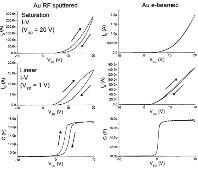
Figure 3-6: Photos of photoresist (PR) residue. The top two photos show photoresist residue after the transistors are completely patterned. The bottom two photos show that the photoresist residue is present right after the via patterning step... 51 Figure 3-7: Illustration of polymerization of photoresist (PR) during RIE oxygen plasma etch. (a) The PR with positive slope will have a region where the polymerized PR is attached to the parylene. (b) In contrast, PR with negative slope does not have any region where the polymerized PR is in contact with the parylene because of the directional nature of the RIE plasma. (c,d) During photoresist removal step, the PR stripper cannot solvate the hardened PR. (d) For the PR with negative slope, the PR stripper undercuts the PR and removes it com p letely ... . ..-- .. 5 2 Figure 3-8: Hysteresis in OTFTs sputtered with vs. e-beamed gold S/D layer. The data in the right column are data from e-beamed S/D layer and show significantly less hysteresis as well has higher current levels. W /L = 1000/25 m . ... 54 Figure 4-1: Operation and symbol of a pentacene OTFT ... 58 Figure 4-2: Sequence of measurements showing the definition of hold time, delay time, and integration time for single and double sweeps... 59 Figure 4-3: Model for calculating time constants for measuring accurate current... 60 Figure 4-4: Transfer characteristics of six different devices in linear (VSD = 1 V) and
saturation (VSD = 30 V) region. The VT is the VSG that the current deviates from a line in the
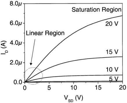
semilog plot. The inverse slope of the line is the S [V/dec]. ... 63 Figure 4-5: Output characteristics of an OTFT. The left region where VSD < VSG - VT is the
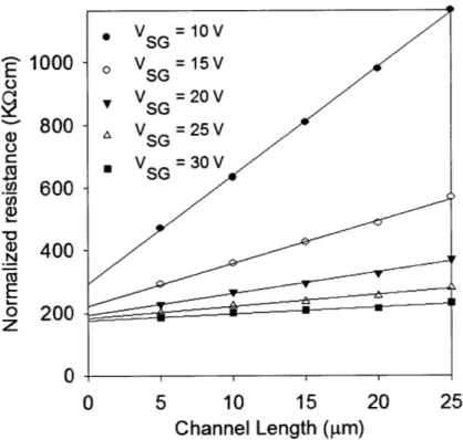
lin ear region ... 6 4 Figure 4-6: Extraction of contact resistance using the TLM. The resistance extrapolated at L
- 0 is the contact resistance. The data is denoted by symbols, and solid lines are fits made for
each gate voltages. ... 66 Figure 4-7: Extracted mobility according to a simplified physical model in Equation (4-7). (a) Not accounting for the contact resistance. (b) Accounting for the contact resistance. If the contact resistance is not accounted for, the mobility decreases severely on shorter channel-length devices. This is because devices with shorter channel channel-lengths are affected more by the contact resistance. In addition the mobility for 5 Rm device looks as if it is constant with respect to the gate voltage. This is not true once the mobility is corrected for the contact resistan ce ... 6 9
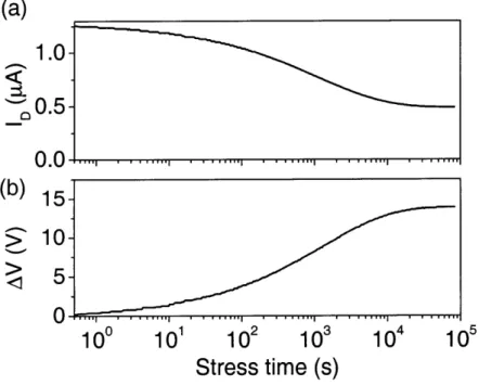
Figure 5-1: Change in the drain current due to the BSE. The plot shows normalized drain current measured at VSG = 10 V, VSD = 1 V during stress phase (VSG = 30 V applied between
measurements), and recovery phase (VSG = 0 V) in nitrogen ambient. When stress is applied,
Figure 5-2: I-V transfer characteristics before, after stress, after 100 s of recovery, and after a day of recovery. The stress condition was VSG = 30 V for 100 seconds. Recovery is performed by grounding the terminals in the dark. Transfer characteristics were taken at VSD
= 1 V. Measurements were taken on a W/L = 1000/25 pm device in nitrogen ambient in the
d ark . ... 7 5
Figure 5-3: Defect creation mechanism in a-Si:H. Weak Si-Si bonds are broken upon occupation of two electrons and stabilized with movement of the hydrogen from a nearby site. The process causes two new dangling bonds which act as electron trap sites... 78 Figure 5-4: (a) Transfer characteristics in the linear region before and after stress. (b) Transfer characteristics in the saturation region before and after stress. The dotted green line shows the original I-V characteristics shifted by 1.8 V to the right for visual aid for comparisons. The data indicates that I-V characteristics after stress can be characterized by a shift in the gate voltage for both linear and saturation regions. The stress condition was VSG = 30 V ,V SD = 1 V for 100 s... ... 80
Figure 5-5: Transfer characteristics as a function of the stress time. The I-V transfer characteristics are taken by interrupting the bias stress. The stress condition is VsG = 30 V, VSD = 1 V. The dashed lines show the shifted transfer characteristics of the fresh device for
v isu al aid ... 8 1
Figure 5-6: Flow chart for the I-V stress characterization method... 82
Figure 5-7: Mechanisms for the BSE and its recovery. The mechanism has two parts where the hole transports to the vicinity of the trap and then is trapped... 83
Figure 5-8: (a) Plot of AV after stress and recovery for different length transistors. The device is stressed for 5 minutes at VSG = 30 V and then grounded for 5 minutes to recover. (b)
Recovered AV after five minutes of recovery... 84 Figure 5-9: AV measured after different stress VSG condition. Measurements are taken on fresh 1000/5 pm devices with VSD = 1 V, stress time = 100 s at room temperature. The solid line is a fit m ade according to Equation (5-1)... 85
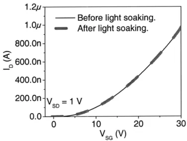
Figure 5-10: I-V measurement before and after soaking OTFT in microscope light for 10 minutes. No change in I-V characteristics is observed... 86
Figure 5-11: (a) AV vs. stress VSD at t = 600 s. The Vso during stress was held at 30 V. The
induced AV decreases with increasing VSD- (b) Data replotted in normalized charge.
Q
is calculated with equation (5-2) and Qo = Ci(VSG - VTO). The solid line represents a linear fit. ... 8 7Figure 5-12: Flow chart for measuring AV using the on-the-fly stress characterization m eth o d ... 8 8
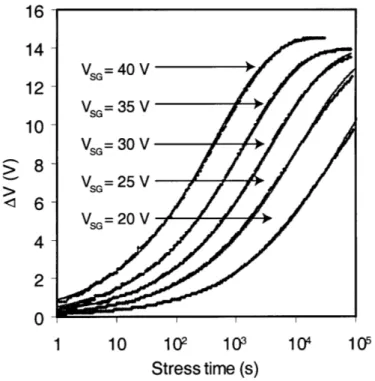
Figure 5-13: (a) The current measurement during stress condition of VSG = 35 V, VSD = 1V at
20 0C, and (b) the extracted AV using the on-the-fly stress characterization method. ... 89
Figure 5-14: Stress time dependence of the induced AV for various gate bias-stress conditions. Each stress condition has fifty data points per decade. The solid green lines, representing the stretched-exponential fit made to the data, are plotted on top of the data.... 90 Figure 5-15: The gate voltage shift for a-Si:H TFTs subjected to various stressing voltages in dicated vs. tim e... 9 1
Figure 5-16: Accelerated stress measurement at VSG = 10 V, VSD = 1 V, and 50 C... 96
Figure 5-17: Stress time dependence of the induced AV for various gate bias-stress conditions. Each stress condition has fifty data points per decade. The solid lines, representing the stretched-exponential fit made to the data, are plotted on top of the data.... 97 Figure 5-18: The plot of t vs. VSG for both p < NT and p > NT region. t drops precipitously with increasing VSG above 14 V (p = NT )... 98 Figure 5-19: Verification of the DOS extraction tool. (a) The log-normal distribution of DOS which is used to generate simulated data in (b) according to Equation (5-12). (c) The DOS extraction tool finds the optimal DOS that fits the simulated data best. Both simulated data and the fit are shown. (d) The extracted DOS match the input DOS well indicating that DOS can be correctly extracted from the extraction tool. ... 100 Figure 5-20: (a) Plot of two stretched-exponential responses with different P. (b) Plot of the extracted DOS from the two stretched-exponential equations. DOS with lower 0 is more disp ersed . ... 10 2 Figure 5-21: (a) Plot of two stretched-exponential responses with different T. (b) Plot of the extracted DOS from the two stretched-exponential equations. The shape of the DOS is not
changed. The two DOS' are offset by an order of magnitude of Ttrap... 103
Figure 5-22: An example trapping mechanism. The carrier must hop over a barrier in order to access the traps, which in this case are dangling bonds in the parylene. The energy barrier as well as the energy level of the trap is dispersed due to the disorder in the material... 104 Figure 5-23: Stress measurements at different temperatures. VSG = 35 V, VSD = 1 V is applied
for bias stress. Measurement results are shown in dots and the fits to the stretched-exponential equation are shown in solid lines. ... 105
Figure 5-24: Illustration of the relationship between DOS vs. E and DOS vs. ttrap at different temperatures. A single DOS vs. E can lead to different DOS vs. Ttrap. In the illustration, the temperature T1 is less than T2, and the DOS for T1 is more dispersed than DOS for T2
because the DOS is spread over a large range of Ttrap resulting in lower
1
and higher T for T1.Figure 5-25: Arrhenius plot for extraction of activation energy as a function of AV. From the measured stress data in Figure 5-23, the time to reach a fixed AV is measured and plotted for each temperature. The activation energy is extracted from the slope of the linear fit to the data as illustrated for AV = 1 V . ... 107
Figure 5-26: The activation energy of the bias-stress time to induce AV. The activation energy is the energy barrier associated with the trap that fills at different levels of AV. The density of trapped carriers is calculated from the measured AV and labeled on the top axis.
... 10 8
Figure 5-27: Extracted DOS from different temperature stress measurements from Figure
5-23. (a) As a function of time constants. (b) As a function of energy barrier. The extracted DOS matches one another indicating that the trapping at different temperature can be
predicted by a single DOS distribution with respect to energy. ... 110
Figure 5-28: Log-log plot of t vs. VSG. t for the stretched-exponential equation can be modeled by T = aVSG - ---...
112
Figure 5-29: AV vs. stress VSG at t = 100 s. The VSD during stress was held at 1 V. Each stress condition is repeated three times, each time on a fresh device. The solid line is AV predicted by E quation (5-15)... 112 Figure 5-30: The circuit lifetime calculated for the case where circuit lifetime threshold is AV
= 1 V . ...
1 15
Figure 5-31: The circuit lifetime calculated for the case where circuit lifetime threshold is
AV/VDD = 10% ...-.---. --- ' ---...1 16 Figure 5-32: Pulsed gate measurements. VDD = 20 V... 117
Figure 6-1: Transfer I-V characteristics before stress, after stress, and after 100s, and 1 day in nitrogen in the dark with all the electrodes grounded. The bias stress condition was VSG = 30 V, VSD = 1 V for 100 s. The measurement is taken on a 1000/25 pm transistor in nitrogen ambient. (top) Linear and (bottom) semilog plots show that the recovered I-V characteristics
are identical to the original I-V characteristics... 125 Figure 6-3: Time dependence measurement of recovery of stressed devices. The solid line is the fit to a stretched-exponential equation... 128 Figure 6-4: Comparison of stress measurements (a) and recovery measurements (b) in devices on different wafers. Devices on annealed wafer have both slower BSE and recovery.
Both devices are stressed to AV = 5 V, and recovered at 40 C. ... 129
Figure 6-5: Temperature vs. recovery after equal stress of VSG = 35 V, VSD = 1 V for 1000 s
Figure 6-6: AV vs. recovery time at the respective temperatures. The transistors are first stressed until AV = 5 V. The dots represent the data and the lines represent the fit to the
stretched-exponential equations... 131 Figure 6-7: Arrhenius plot of t vs. 1/kT for the extraction of activation energy for . ... 131 Figure 6-8: Recovery as a function of time. Every 600 seconds the gate voltage during the recovery phase is stepped up starting from 0 V to 15 V. It is found that stepping up the VSG
from -5 V to -10 V and from -10 V to -15 V significantly increase the recovery rate. M easurem ents w ere taken at 40 C ... 132 Figure 6-9: Direct measurement of the recovery rate by measuring charge due to detrapped carriers. Measurement set up during stress (left) and during recovery (right). Recovery is measured by monitoring the voltage at the gate. ... 133 Figure 6-10: Charge measurement for different temperatures. A stress of 300 seconds at VSG
= 30 V, VSD = 1 V is applied to the device before the charge measurement. The detrapping
charge in the channel induces a drop in the gate voltage. The rate is slowed as the tem perature decreases. ... 134 Figure 6-11: Charge measurement from a MIM capacitor and an OTFT. The voltage change due to detrapping of the trapped carriers during recovery phase is measured. The voltage is normalized by the area of each device. The MIM capacitor shows no significant change in the voltage compared to the OTFT indicating that the traps are located at the parylene/pentacene interface...135 Figure 6-12: Stress-recovery-stress measurement. The AV is plotted throughout the measurement. The OTFT is first stressed for 5000 s at VSG = 35 V, VSD = 1V, and recovered
for a 50000 s and stressed at identical stress conditions for a second time. At 40 C. ... 136 Figure 6-13: Repeated stress measurements. AV data from Figure 6-12 are replotted with respect to the stress time. The second stress measurement has some residual AV left from the previous stress measurement. It can be noted that the trapping rate has not increased and the
BSE saturates at the same AV. All measurements were taken at 40 0C... 137
Figure 6-14: Band diagram for (a) VsG > 0, (b) VSG = 0, and (c) VSG < 0. The energy for
holes are drawn, with a reference energy with respect to the vacuum level. Trapping is shown in (a), and detrapping is shown in (b) and (c). The trapping occurs by channel carriers hopping over a barrier to access the defect states. The recovery occurs by release of the trapped carrier over a barrier in the reverse direction. The Fermi energy in the channel is modulated by the VSG and dictates whether trapping or recovery occurs. ... 139 Figure 6-15: Representation of traps spatially distributed through the channel. The conduction is mainly due to the states which are spatially and energetically close to one another (connected lines in the middle). The states are shown only in the spatial domain for illustrative purposes. Due to the disorder, there are states that may be spatially and energetically isolated from the nearest neighbors (circled states). These spatially isolated
states can take long for carrier population to equilibrate to the Fermi level and can act as trap states that cause the B SE ... 140 Figure 7-1: Linear I-V characteristics change due to post-process anneal at different temperatures. Measurements were done on a 1000/5 ptm device with VSD = 1 V ---... 144
Figure 7-2: Contact resistance extraction before and after the PPA. The slope of the line, which is inversely proportional to mobility, has not changed indicating that the mobility has not changed while the y-intercept, which is the contact resistance, has increased by four folds. PPA condition was 120 0C in nitrogen for ten minutes. ... 145
Figure 7-3: I-V characteristics with and without the APDP process... 146 Figure 7-4: The contact resistance extraction of devices with and without the APDP process. The slope of the line, which is inversely proportional to mobility, is reduced indicating an increase in mobility. APDP condition is 120 0C in nitrogen for ten minutes... 146
Figure 7-5: The BSE on devices with and without APDP. The APDP devices have less AV after the sam e bias-stress conditions... 147 Figure 7-6: AFM on unannealed and annealed parylene. Height image is shown in the left and phase image is shown in the right column. There is no discernable difference in height image, but the phase image is different indicating that the surface energy is different. The scan area is 1 pm x 1 pm. Height range = 10 nm, phase range = 500 ... 148 Figure 7-7: Water contact angle measurements on parylene. (a) before annealing (b) after annealing. After annealing, parylene has higher contact angle indicating a lower surface en erg y ... . ---... 14 9 Figure 7-8: Extended time stress measurements for annealed transistors at 40 0C. Stress condition is V SG = 35 V , V SD = 1 V ... 151
Figure 7-9: Temperature dependence of bias-stress in annealed transistors. Stress condition is V SG= 35 V , V SD = 1 V ... 151
Figure 7-10: Activation energy for data in Table 7-4. The activation energy for APDP transistors is 0 .7 eV ... ... 152 Figure 8-1: Fabrication of OTFTs using separate growth of organic semiconductor thin films. In such an approach, the effect of the semiconductor film morphology and the dielectric can b e sep arated...--. 15 8 Figure 8-2: Integrated process of OTFTs with hybrid organic/metallic encapsulation... 160
List of Tables
Table 2-1: Features of different large-area compatible patterning methods... 33 Table 3-1: Comparison of parylene N and parylene C. Parylene N exhibits no change in dielectric constant with respect to frequency. The changing dielectric constant in parylene C causes complications when interpreting the BSE in OTFTs with parylene C dielectric... 48 Table 5-1: Fit parameters to different VSG stress conditions in the stretched-exponential m o d el... . . ---... 9 0 Table 5-2: Fit parameters to low VSG stress conditions in the stretched-exponential model.. 97
Table 5-3: Fit parameters to different temperature stress data to the stretched-exponential eq u ation...--- - 10 5 Table 5-4: Lifetime measurements for VDD = 20 V when the gate is stressed with a DC bias, and pulsed gate bias. The lifetime from the pulsed gate bias is 50 times longer in both scenarios of circuit lifetim e calculations... 117 Table 7-1: Parameter comparison before and after the PPA. The extracted parameters show
that the degradation is caused by the increase in the contact resistance. Measurements were taken on the sam e devices... 145 Table 7-2: Parameter comparison of devices with and without APDP. The APDP devices have less contact resistance and higher m obility. ... 147 Table 7-3: Results from different annealing times. ... 150
Chapter 1
Introduction
Organic thin-film transistors (OTFTs) that use organic semiconductors as the active layer are promising for large-area flexible electronics. Once only an academic research topic because of their low mobility, they now have sufficient electronic performance for many applications. For example, flexible backplanes for OLED and LCD displays and new electronic Braille sheets have been demonstrated with OTFTs [1,2,3]. In addition, they can be deposited from solutions, which makes them compatible with low-cost manufacturing methods such as roll-to-roll processing. Companies such as Plastic Logic and PolyIC are preparing to launch the first commercial applications based on solution processed organic transistors [4,5].
Thin-film transistors (TFTs) are a key component in every active-matrix liquid crystal display (AMLCD). Most TFI's currently use thin hydrogenated amorphous silicon (a-Si:H) as the active layer. Due to the disorder in amorphous silicon, a-Si:H TFTs have mobility about a hundred times smaller than traditional single crystalline silicon metal-oxide-semiconductor field effect transistors (MOSFETs). Despite such a drawback, TFTs dominate large-area applications because they can be deposited on large glass substrates, which is not possible with single crystalline silicon MOSFETs due to their high processing temperatures
The state of the art, Generation 10 LCD plants use a-Si:H TFTs on glass substrates that are 2.85 m by 3.05 m [6].
Figure 1-1: Exhibition of Gen 10 (= 2850 x 3050 mm) glass for AMLCDs.
TFT' technology has found a niche in LCDs where the performance requirements are not high and the large area capability is absolutely necessary. Initially, passive-matrix LCDs were most widespread because of their simplicity. However, passive-matrix LCDs are limited in size due to the leakage current and noise characteristics in the liquid crystals (LCs) [7]. In AMLCDs, TFTs are used as switches to access the individual pixels and reduce parasitic leakage current through the LCs by orders of magnitude so that more columns can be driven in a display. Also, they increase the yield of the completed display because a single short in a pixel does not result in the entire column being shorted as it does in passive-matrix LCDs. The ability to drive more rows and increase yield made TFTs critical in large, high information density LCDs - an industry that has grown to a $30 billion-a-year business [8]. The dominant TFT technology used in AMLCD today is a-Si:H TFT technology.
Passive Matrix Active Matrix
Column Data (pixel brightness) Column Data (pixel brightness) Row Select Row Select Row Select (Defective Ro
--- p---'
w) _-7
t ~ E Y;Z; ~ ; v;7 Row Select Defective LC Defective LCFigure 1-2: Passive-matrix vs. active-matrix backplane. In passive-matrix configuration, the
LC leaks current from data line to the row select line. The total leakage current to the row
select line increases with number of columns and limits the number of columns. In active-matrix configuration, there is no such limit because the leakage current is controlled by a TFT. Also in a passive-matrix backplane, a defective LC results in the whole row being defective whereas in active-matrix, a defective LC only affects a single pixel.
1.1
Problem Statement
With the maturing LCD industry, interest has risen in using TFTs for new flexible large-area electronics which are made on plastic substrates. Plastic substrates can be used to make
light-weight rugged displays which are easy to transport and do not shatter. Large rugged displays which can be rolled up to fit in a pocket have been envisioned for mobile and military applications as shown in Figure 1-3. Other applications such as imagers with curved surface to relax requirements on lens design [9] and flexible sensors which can sense temperature
and pressure over large area have been proposed for robotic skins [10].
There are a number of requirements that must be met in order to realize flexible electronics on plastic substrates. First of all, the device must be flexible. Single crystalline devices cannot be bent because bending them will typically shatter them. Secondly, the processing temperature must be low or a thermal barrier layer must be developed so that the underlying plastic substrate is not degraded. If the processing temperature is kept below 150 0C a number of electronic-grade plastic substrates can be used as shown in Figure 1-4 [11].
Figure 1-3: (a) A concept of rollable display for mobile applications. Courtesy of Phillip Spears and HP. (b) Flexible temperature and pressure sensors for robotic skins [7].
400 350
0 - PET -poly(ethylene terephthalate)
E 200- PEN -poly(ethylene naphthalate)
4 150- HS - heat stabilized 100- PC - polycarbonate 0- PES - poly(ethersulphone) PAR - polyarylates q
o<90
P < PI -polyimide d0V PolymerFigure 1-4: Glass transition temperature of electronic-grade plastic substrates [11]
Conventional a-Si:H TFTs do not meet this requirement as they require processing temperatures typically around 200-300 *C [12]. Lastly, there are other requirements relating to the manufacturing cost and yield that need to be met for practical applications.
Organic TFTs meet all these requirements for flexible electronics. Recently, Sekitani and Someya have fabricated OTFIs with mobility of 0.58 cm2/Vs and on/off ratio of 105 on flexible polyimide (PI) films [13]. They demonstrate that these transistors exhibit only 4% change in mobility when rolled to a radius of 2 mm and can be stored in air without much degradation if proper encapsulation is applied.
However, OTFIls exhibit the bias-stress effect (BSE) which causes operational instability that limits them from being used in a wide range of circuit applications. The BSE refers to the change in characteristics of the transistors due to application of electric bias stress. The
BSE causes drain current degradation in TFTs which leads to circuit failures that limit the
lifetime of the circuit. For any applications that use OTFTs as analog circuit elements, the 21
BSE needs to be addressed. One example is the backplane for organic light-emitting-diode (OLED) displays. OLED technology is the next generation display technology that consumes
less power, has more vibrant color, higher contrast, and simpler device structure than LCDs
[14]. However, in contrast to LCDs, OLEDs require constant current to drive them.
Therefore the transistors are used as constant current sources. The change in TFT characteristics results in direct degradation of the picture quality, and thus more stable TFTs or a compensation scheme for the BSE needs to be considered [15]. For practical usage in a wide array of applications, the BSE needs to be reduced.
This work aims to develop a methodology to characterize the BSE in OTFTs and characterize it with respect to various stress conditions and investigate the cause of the BSE in pentacene OTFTs by means of electrical characterization methods. Pentacene is chosen as the model organic semiconductor because it is the most widely studied organic semiconductor for OTFTs owing to its high mobility and robustness. The effect BSE has on circuit lifetimes is studied, and careful measurements are taken to identify the physical source of the BSE. Afterwards, a method to reduce the BSE is developed, and the cause of the improved stability is investigated.
1.2
Structure of Thesis
The thesis is structured as follows. We begin by introducing the basic theory of operation of OTFTs in Chapter 2. In Chapter 3, the process for integrated pentacene OTFTs developed at MIT is described in detail. The process has been used to prepare samples measured in this
work. We underline the key decisions leading to the use of various processes and physical characteristics of the dielectric and the semiconductor. Chapter 4 then discusses key characterization methods in OTFTs. In Chapter 5 we characterize the BSE in OTFTs with the use of the characterization methods introduced in Chapter 4 for various parameters. We investigate the dependence on channel length, temperature, and bias voltage during stress and discuss the implications of these results to circuit lifetime. Chapter 6 measures the recovery from the BSE after the bias stress is removed. Chapter 7 introduces a new annealing procedure that reduces the BSE. A series of measurements is performed to identify the source of the reduced BSE. Finally, Chapter 8 summarizes the accomplishments of this work and contains suggestions for future work.
REFERENCES IN CHAPTER 1
[1] M. Mizukami, N. Hirohata, T. Iseki, K. Ohtawara, T. Tada, S. Yagyu, T. Abe, T. Suzuki, Y. Fujisaki, Y. Inoue, S. Tokito, and T. Kurita. Flexible AM OLED panel driven by bottom-contact OTFTs. IEEE Electron Device Lett. 27:249, 2006.
[2] K. Nomoto, N. Hirai, N. Yoneya, N. Kawashima, M. Noda, M. Wada, and J. Kasahara.
A high-performance short-channel bottom-contact OTFT and its application to AM-TN-LCD. IEEE Trans. Electron Devices, 52:1519, 2005.
[3] Y. Kato, T. Sekitani, M. Takamiya, M. Doi, K. Asaka, T. Sakurai, and T. Someya. Sheet-Type Braille Displays by Integrating Organic Field-Effect Transistors and Polymeric Actuators. IEEE Trans. Electron Devices, 54:202, 2007.
[4] D. Sabbagh. 'Moving newspaper' on flexible screen to be launched within months. The
Times. Online source. Available at: http://business.timesonline.co.uk/tol/business/ industry sectors/technology/article6736859.ece, August 3, 2009.
[5] C. Hammerschmidt. RF energy powers printed lighting device. EE Times Europe.
Online source. Available at: http://eetimes.eu/showArticle.jhtml?articlelID=218600728, July 27, 2009.
[6] H. Kachi. Update: Sharp to up Kameyama LCD panel output capacity 10%. Wall Street Journal. Online source. Available at: http://online.wsi.com/article/BT-CO-20090709-703378.html, July 9, 2009.
[7] P. Alt and P. Pleshko. Scanning limitations of liquid-crystal displays. IEEE Trans.
Electron Devices, 21:146-155, 1974.
[8] T. Tsukada, Active-Matrix Liquid Crystal Displays in Technology and Applications of
Amorphous Silicon, R. A. Street (Ed.), Springer Verlag Heidelberg, 2000.
[9] H. C. Ko, M. P. Stoykovich, J. Song, V. Malyarchuk, W. M. Choi, C.-J. Yu, J. B. Geddes, J. Xiao, S. Wang, Y. Huang, and J. A. Rogers. A hemispherical electronic eye camera based on compressible silicon optoelectronics. Nature, 457:706-710, 2009.
[10] T. Someya, T. Sekitani, S. Iba, Y. Kato, H. Kawaguchi, and T. Sakurai. A large-area,
flexible pressure sensor matrix with organic field-effect transistors for artificial skin applications. Proc. Natl. Acad. Sci., 101:9966, 2004.
[11] W. A. MacDonald, Advanced Flexible Polymeric Substrates in Organic Electronics, H.
Klauk (ed.), pp. 165, Wiley-VCH, 2006.
[12] J.I. Pankove, Semiconductors and Semimetals: Hydrogenated Amorphous Silicon, Part D: Device applications. pp. 9, Academic Press, New York, 1984.
[13] T. Sekitani and T. Someya. Air-stable operation of organic field-effect transistors on
plastic films using organic/metallic hybrid passivation layers. Jpn. Jnl. Appl. Phys., 46:4300-4306, 2007.
[14] J. Yu. Improving OLED Technology for Displays. PhD Thesis, MIT, Cambridge, 2009.
[15] S. Ashtiani , J. Shahin , P. Servati , D. Striakhilev and A. Nathan. A 3-TFT
current-programmed pixel circuit for AMOLEDs. IEEE Trans. Electron Devices, 52:1514, 2005.
Chapter 2
Introduction to OTFTs
Organic semiconductors have been studied as early as the late 1940s [1]. In 1948, Eley and Vartanyan have reported experimental studies of dark conductivity in phthalocyanines. Beginning in 1980s, organic TFTs based on polymer and small molecule semiconductors have been studied. However the performance of these devices was poor and the interest in OTFTs remained largely an academic curiosity. Through the research of better materials and device structures, OTFTs with mobility surpassing that of a-Si:H have been demonstrated in the late 1990s [2]. Figure 2-1 shows the progress of the largest reported mobility from 1986 to 2006. The performance of small molecule organic semiconductors is better than that of polymer semiconductors, and both have shown impressive progress in the last two decades.
10'
S100
I10.1
I10-5
Figure 2- 1: Improvement of mobility in organic semiconductor over the years. Rates of mobility increase have been similar for single crystals, polymers and small molecules. [3]
The research result of OTEL's with comparable performance to a-Si:H TiFfs generated great interest in both academia and industry because organic semiconductors had several key advantages compared to amorphous silicon. First, the substrate can be at room temperature during the deposition step as organic semiconductors can be evaporated at low temperatures owing to their van der Waal bonds which are substantially weaker than covalent bonds. This low temperature deposition opened up the exciting possibility of integrating electronics on surfaces that were not available for electronics before. A number of groups have demonstrated functional transistors on various flexible substrates including plastics [4] and even on paper [5].
Secondly, various physical properties such as the band gap and surface affinity of organic semiconductors can be controlled with the synthesis of new organic semiconductors. Such controllability can be used to make organic semiconductors that emit different colors of light for OLEDs and semiconductors that respond selectively to chemicals for sensing chemicals. In addition, this controllability allows the use of molecular self-assembly to enable highly ordered films without the need to anneal or increase deposition temperatures. This controllability is possible because larger molecular building blocks are used instead of atoms.
Thirdly, organic semiconductors can be deposited via solution processing. The solution deposition process allows OTFTs to be printed using conventional low-cost patterning methods in a roll-to-roll fashion akin to printing newspapers. The solution processing methods are envisioned to lower the manufacturing cost of electronics per area. Although solution processing has been performed mostly with polymer semiconductors, many groups have shown small molecule organic semiconductors can be also deposited via solution process by modifying the side groups to tune the solubility of organic semiconductors. Moreover, recent research has shown that even small molecules like pentacene with limited solubility in organic solvent can be used to fabricate high performance (j > 0.5 cm2/Vs) OTFTs from solution deposition [6]. These three key advantages of room temperature deposition, tunable semiconductor properties, and low cost patterning methods provide exciting research opportunities for OTFTs.
2.1
Structure of OTFTs
OTFTs consist of at least five different layers. The substrate provides mechanical support as the thickness of the individual films is typically less than a micron each. Additionally, there are the gate, dielectric, source-drain, and semiconductor layers. The gate layer is separated from the semiconductor layer by the dielectric, whereas the source-drain layer is in direct contact with the semiconductor. The contact is necessary to inject and extract carriers from the semiconductor. Some common OTFT structures are shown in Figure 2-2. Depending on the location of the gate and the semiconductor with respect to the substrate, the transistor is categorized into bottom gate (inverted) or top gate (non-inverted) structure. The inverted terminology comes from the fact that the gate is at the bottom, contrary to traditional silicon MOSFETs. Most OTFTs are in bottom gate configuration because organic semiconductors can be easily damaged from processing, and this configuration minimizes processing steps for the organic semiconductors. In addition, depending on the location of the contact with respect to the semiconductor, the transistor is further categorized into bottom contact (coplanar) or top contact (staggered). In OTFTs, a top contact (TC) structure has been reported to have lower contact resistance perhaps due to the penetration of metal dopants into the semiconductor resulting in doped semiconductor contact [7]. However the top contacts can only be deposited through shadow masks which limit the resolution to about 50 jim. Bottom contact (BC) configuration allows the use of conventional photolithographic patterning technique which allows submicron channel-length OTFTs. Photolithographic patterning technique is also the proven scalable large-area technology used for commercial
(a)
Dielectric
Substrate
(b DielectricSubstrate
(c) Dielectric G" SubstrateFigure 2-2: Common OTFIT structures. (a) Top gate, top contact. (b) Bottom gate, top contact. (c) Bottom gate, bottom contact configuration.
In many works, heavily doped silicon wafer is used as the gate layer because it provides an accessible method of fabricating OTFTs. Silicon wafers are commercially available with thermally grown silicon dioxide which can be used as the gate dielectric. Therefore, the use of silicon wafer only requires the growth and patterning of two additional layers to complete the OTFTs. The widely available silane surface treatment for silicon dioxide is also a notable advantage of using heavily doped silicon and silicon dioxide systems. Many research works continue to use silicon substrates with the aim of investigating and improving organic
semiconductor properties [8]. Although such devices serve the need for preliminary research work for new organic semiconductors, they cannot have patterned gates crucial for circuit applications. In addition, the use of thermally grown oxide in flexible or large area electronics is not possible as they require high temperature.
Recent works have started employing different dielectrics that can be deposited at low temperatures. Such dielectrics include spun cast polymers like polyimide [ 9 ], CVD evaporated polymers [10], self assembled monolayer [11], and organic/inorganic hybrid dielectrics [12]. All these dielectrics have been shown to have low interface states such that subthreshold slopes are less than 1V/decade and have sufficient electrical performance with mobility > 0.1 cm2/Vs.
2.2
Fabrication of OTFTs
Fabrication of OTFTs has been demonstrated using a number of techniques [8]. Among many techniques, additive printing methods that are compatible with roll-to-roll fabrication are notable as these methods enable low-cost electronics on large-area flexible substrates. OTFTs with all the layers printed via additive processes have been demonstrated [13]. Additive processes are advantageous compared to subtractive processes because they are simple and have higher material utilization. In a subtractive patterning process, a photoresist must be patterned to the substrate, the patterned layer must be etched, and finally the photoresist layer must be removed to complete the process. An additive process reduces all these steps into a single step, which represents significant savings on cost. Because superior
resolution offered by lithographic patterning is not required for low performance electronics over large area, the printing process is preferred for low-cost large-area applications. There are a number of additive processes available for organic semiconductors in traditional graphical printing methods such as flexography, gravure, offset, and inkjet. Subramanian et
al. have demonstrated a subset of these printing methods for printing electrodes on flexible
surfaces [14]. The table below shows the comparison of various printing methods.
Printing Layer Feature Viscosity Throughput Registration Features/ Examples of technique thickness size (mPas) (m2
S-1) (Pm) issues graphic art
(sm) (prm) applications
Letterpress 0.5-1.5 >50 50000-150000 1 <200 Books Flexography 0.8-2.5 80 50-500 10 <200 Wide range Packaging;
of substrates, newspaper; medium labels quality
Gravure 0.8-8 75 50-200 60 >10 Large run Magazines; length; plastic film high quality and
metal foils; bank notes
Pad 1-2 20 >50 0.1 >10 Nonplanar Toys; CDs;
objects pens Offset 0.5-1.5 10-50 40000-100000 5-30 >10 High Newspapers;
quality; magazines; need for books ink additives
Screen 30-100 20-100 500-50000 2-3 >25 Wide range Textiles; of inks; PCBs; CDs; medium large posters quality
Inkjet <0.5 20-50 1-30 0.01-0.5 5-20 Digital data; Desktop; local variable data registration
Although these new patterning methods are promising, they are not production-ready in terms of yield and reproducibility and need to be improved. Photolithography has been the standard method of fabrication in microelectronics and in large-area electronics with high yields and reproducibility. High yields are necessary to make circuit applications, so the lithographic process is used in this work to study electrical characteristics of OTFTs. The specific process to fabricate OTFTs will be introduced in the next chapter.
2.3
Transport in Organic Semiconductors
Transport in organic semiconductor is a topic of much debate. It has been observed that mobility in OTFTs increases as the field and temperature increase. It has been theorized that in organic single crystals the transport is dominated by hopping [16]. The van der Waal bonds that hold organic molecules together are on the order of 0.1 eV in contrast to 1 eV of covalent bonds resulting in weak interactions of electron wave functions from adjacent molecules. As a result, the carriers are bounded and localized on a molecule which results in hopping transport. The hopping rate increases with field and temperature as the carriers can hop from one state to another state easily in the presence of field and at higher temperatures. The hopping rate from state i to
j
can be generally expressed as the following [17]:rij = vo exp(-Eij/kT)exp(-2yRij) if Ej > Ei
(2-1) rij = vo exp(-2yRij) if Ej < Ei
where rij is the hopping rate, V0 is the attempt frequency, Eij = Ej - Ei, Ei and Ej is the energy
of states i and
j
respectively, Rij is the distance between states i andj,
andy~1
is the decay 34length of the wave functions. Naturally, the hopping transport in organic crystals leads to temperature and field dependence in amorphous and polycrystalline organic semiconductors as well.
Rij
hopping rate:
vij
=
vo exp(-2yRij) exp( -Eij/kT)
Eij
state i
state
j
Figure 2-3: Hopping rate between two states.
However, experimental measurements on different organic single crystals such as naphtlaene, rubrene, and pentacene have been reported to have band transport-like behavior where the mobility decreased as the temperature increased, and the mobility is independent of the gate field [18]. In band transport, mobility decreases as temperature increases because of the increased phonon scattering. Likewise, the field would not have a strong effect on mobility if the carriers are delocalized in extended states. This indicates that transport in organic single crystals may be band transport despite the weak van der Waal bonds between the molecules.
In OTFTs which use disordered film of organic semiconductors, we observe increasing mobility with temperature and field in contrast to what is observed for single crystalline organic transistors. The transport in these disordered materials can be explained with band transport in the framework of trap limited conduction (TLC) model. In TLC model, most of
the induced carriers in the channel are not mobile, and charge transport is dominated by a small number of carriers that are at a relatively high mobility states. Such states can be the extended states where carriers are free to move around. For convenience, the states with high mobility will be referred to as the free states, and the energy at the free states will be denoted as Ev, to make the terminology consistent with the existing silicon literatures. The term Ev is used interchangeably with highest occupied molecular orbital (HOMO) in individual molecules.
In the linear region, the drain current can be expressed as the following:
ID = W q pfree Pfree E (2-2)
where W is the width of the device, q is the charge per electron, pfree is the mobility of the free hole carriers, Pfree is the density of free carriers, and E is the lateral electric field across the channel. Pfree is described by:
Ey
Pfree = Jv (E)(1 - f (E))dE (2-3)
where gv(E) is the DOS near Ev, and f(E) is the Fermi function. (1 - f(E)) is used because
carriers are holes. The Fermi function is expressed as the following: 1
f
(E) = (2-4)1+ exp(-(E - EF)/kT)
where EF is the Fermi energy. Because the Fermi energy is above Ev by more than 3kT,
Boltzmann approximation can be used for f(E) in Equation (2-3) to yield:
Pfree = NV exp(-(EF Ey) kT ) (2-5)
where Nv is the effective density of free states, defined in a similar manner as in Si MOSFETs. From this relationship, the temperature dependence can be established. The current is proportional to pfree which increases proportional to exp(-(EF- E,)IkT). As
temperature increases, the term inside the brackets becomes less negative and pfree increases exponentially.
The measured mobility of the OTFT can be expressed as [19]:
I1OTFT = ffree ree free P free f'ree P free (2-6)
Pinduced P free + Ptrapped Ptrapped
where ptfree is the mobility of the free hole carriers, and pfree and ptrapped are the densities of free and trapped carriers respectively. The approximation in Equation (2-6) is justified because the density of free carriers is small compared to the density of trapped carriers.
Energy En rgy
Er F E F
-1-f(E) DOS
Figure 2-4: Fermi energy level and carrier population at trap states and free states.
ptrapped can be expressed as the integration of DOS and the Fermi function:
Ptrapped = Jgv (E)(1 - f (E))dE (2-7)
EV
The integration from infinity may be troublesome, but gv(E) is usually modeled with a exponential tail states which decreases to 0 as energy is increased, and hence the integration results in a finite number. If the DOS changes gradually with respect to the Fermi function as illustrated in Figure 2-4, the Fermi function can be regarded as a step function where above EF the states are all filled with trapped holes and below EF the states are empty. States are modeled as neutral when empty.
idf
Ptrapped = fgv (E)dE (2-8)
As the Fermi level moves closer to the Ev with increasing VSG, the Ptrapped increases with
gv(E) while the pfree increases exponentially with exp(-(EF- Ey ) / kT) . Therefore the
measured OTFIF mobility increases with increasing VSG. Another way to describe what is occurring as the gate voltage increases is that as more charge carriers are induced in the channel they fill the traps so that trapping becomes less efficient and charge transport
![Table 2-1: Features of different large-area compatible patterning methods. From [15].](https://thumb-eu.123doks.com/thumbv2/123doknet/14157673.472806/33.918.149.786.367.954/table-features-different-large-area-compatible-patterning-methods.webp)

![Figure 3-3: Illustration of the process flow for deposition of Parylene N. From [7].](https://thumb-eu.123doks.com/thumbv2/123doknet/14157673.472806/47.918.159.789.581.802/figure-illustration-process-flow-deposition-parylene-n.webp)