Designing nonvolatile integrated photonics
with low-loss optical phase change materials
The MIT Faculty has made this article openly available.
Please share
how this access benefits you. Your story matters.
Citation
Zhang, Yifei et al. "Desigining nonvolatile integrated photonics with
low-loss optical phase change materials." Proceedings of SPIE
- The International Society for Optical Engineering, September
2019, San Diego, California, The International Society for Optical
Engineering, 2019, DOI: 10.1117/12.2528993 © 2019 SPIE.
As Published
10.1117/12.2528993
Publisher
SPIE
Version
Final published version
Citable link
https://hdl.handle.net/1721.1/129737
Terms of Use
Article is made available in accordance with the publisher's
policy and may be subject to US copyright law. Please refer to the
publisher's site for terms of use.
PROCEEDINGS OF SPIE
SPIEDigitalLibrary.org/conference-proceedings-of-spie
Designing nonvolatile integrated
photonics with low-loss optical phase
change materials
Zhang, Yifei, Zhang, Qihang, Chou, Jeffrey, Li, Junying,
Roberts, Christopher, et al.
Yifei Zhang, Qihang Zhang, Jeffrey B Chou, Junying Li, Christopher Roberts,
Myungkoo Kang, Claudia Gonçalves, Richard Soref, Carlos Ríos, Mikhail
Shalaginov, Kathleen Richardson, Tian Gu, Vladimir Liberman, Juejun Hu,
"Designing nonvolatile integrated photonics with low-loss optical phase
change materials," Proc. SPIE 11081, Active Photonic Platforms XI, 110811S
(12 September 2019); doi: 10.1117/12.2528993
Event: SPIE Nanoscience + Engineering, 2019, San Diego, California, United
States
*[email protected]; phone 1 617-955-9718.
Designing Nonvolatile Integrated Photonics with Low-loss Optical
Phase Change Materials
Yifei Zhang
1, *, Qihang Zhang
1, Jeffrey B. Chou
2, Junying Li
1, Christopher Roberts
2, Myungkoo
Kang
4, Claudia Gonçalves
4, Richard Soref
3, Carlos Rí
os
1, Mikhail Shalaginov
1, Kathleen
Richardson
4, Tian Gu
1, Vladimir Liberman
2, Juejun Hu
11
Department of Materials Science and Engineering, Massachusetts Institute of Technology,
Cambridge, MA, USA
2
Lincoln Laboratory, Massachusetts Institute of Technology Lexington, Massachusetts, USA
3Department of Engineering, University of Massachusetts Boston, Boston, MA, USA
4College of Optics and Photonics, University of Central Florida, Orlando, Florida, USA
ABSTRACT
The development of low-loss optical phase change materials (O-PCMs) promises to enable a plethora of nonvolatile integrated photonic applications. However, the relatively large optical constants change between different states of calls for a set of new design rationales. Here we report a non-perturbative design that enables low-loss device operation beyond the traditional figure-of-merit limit. The basic design rationale is to engineer the light propagation path through the O-PCMs when it is in the low-loss amorphous state, and divert light away from the lossy crystalline state leveraging the large mode modification induced by the O-PCM phase transition. Following this approach, we demonstrate broadband photonic switches with significantly enhanced performances compared to current state-of-the-art.
Keywords: Low loss phase change materials, nonvolatile photonics, integrated photonics
1. BROADBAND LOW-LOSS OPTICAL PHASE CHANGE MATERIALS
Chalcogenide optical phase change materials, such as Ge-Sb-Te (GST) compounds, have been studied for a plethora of emerging optical applications including photonic memories, reconfigurable metasurfaces, optical switching and non-volatile displays1-5. These traditional phase change materials, however, generally suffer from large optical losses even in
their dielectric states. For instance, GST is optically absorbing at the telecommunication bands due to its high inter-band absorption, whereas its crystalline state is plagued by high free carrier absorption (FCA) in the mid- and long-wave infrared regime (Fig. 1a). The large optical losses fundamentally limit the performance of photonic devices based on these O-PCMs. We define the material figure-of-merit (FOM) for O-PCMs as: FOM = n/k, where n denotes the index change upon
phase transition and k is the extinction coefficient. It can be shown that this FOM quantitatively dictates the attainable insertion loss and contrast ratio of tunable optical devices based on O-PCMs6.Current O-PCMs solutions generally suffer
from poor FOM’s – mostly in the order of unity. This imposes a major challenge towards their optical applications. In order to tackle this challenge, we have recently developed a new class of O-PCMs, Ge-Sb-Se-Te (GSST) alloys. Fig.1b-d plot the refractive inFig.1b-dex (n) anFig.1b-d extinction coefficient (k) Fig.1b-dispersions measureFig.1b-d for the chalcogeniFig.1b-de thin films with a varied Se-to-Te atomic ratio at their amorphous (Fig. 1b) and crystalline (Fig. 1c) states. Among the studied compositions, Ge2Sb2Se4Te1 (further in the text abbreviated as GSST) demonstrates the highest FOM~100, which stems from its large
Δn of 1.2 – 1.5 across the near- to mid-IR bands while maintaining low optical loss at both structural states from 2 – 7 μm, as shown in Fig. 1d. The optical loss of GSST is two orders of magnitude lower than that of the classical phase change alloy GST-225. The remarkable low-loss performance benefits from blue-shifted interband transitions as well as minimal free-carrier absorption due to significantly reduced free carrier concentration and mobility.
To demonstrate the advantages of reduced optical loss, we show a narrow band ON/OFF photonic switch: a SiN ring resonator coupled to a bus waveguide, with GSST on top. SEM image of the structure is shown in Fig. 2a. We deposited a 50-nm thick strip of GSST on top of the resonator as depicted in the inset to Fig. 2a. Phase transition of O-PCMs was controlled by annealing and confirmed via Raman spectroscopy. Fig. 2c plot the transmittance spectra of SiN micro-ring devices integrated with the O-PCM alloys when they are switched from amorphous to crystalline state. The device
Best Student Paper Award
Active Photonic Platforms XI, edited by Ganapathi S. Subramania, Stavroula Foteinopoulou, Proc. of SPIE Vol. 11081, 110811S · © 2019 SPIE · CCC code: 0277-786X/19/$21
doi: 10.1117/12.2528993 Proc. of SPIE Vol. 11081 110811S-1
integrated with the GSST material claims a large on/off contrast ratio of 41 dB and a reduced insertion loss of 0.2 dB, both of which represent significant improvements compared to state-of-the-art GST-based device7, 8. As a reference, we
fabricated and characterized a similar device with a strip made of conventional GST-225 instead of GSST. Fig. 2b shows that the reference device in the “off” state still had a transmittance dip, i.e. the strip did not completely turn off even when GST-225 was transformed into crystalline state. Such remarkable performance is also supported by the theoretical studies based on the measured optical constants of GSST and can be attributed to its exceptional FOM.
Figure 1. (a) Optical absorption of the classical phase change alloy Ge2Sb2Te5 fitted to show combined contributions from interband transition, Urbach tail, and FCA based on Drude models. (b, c) Measured real (n) and imaginary (k) parts of refractive indices of the (b) amorphous and (c) crystalline alloys. (d) Optical properties of amorphous (dashed lines) and crystalline (solid lines) Ge2Sb2Se4Te1 from the visible range to LWIR. Data from reference [9] and [10].
Figure 2. (a) SEM images of fabricated ring resonator devices. (b, c) Transmission spectra of (b) GST-based device and (c) GSS4T1-based device. (a-c) Reproduced from [10]. Copyright 2017, Optical Society of America.
2. NON-PERTURBATIVE DESIGN FOR O-PCM PHOTONIC SWITCHES
An optical switch is a key component of dynamic integrated photonic circuitry11-14. In this section, we report the design
and modeling of a new kind of design principle for broadband on-chip photonic switches combining low-loss phase change alloys and a “non-perturbative” design to boost the switching performance15. The FOM of GSST is pre-dominantly limited
c-GST but still pretty high for guided-wave devices. The large index contrast between the two phases in GSST enables us to evaluate new designs to circumvent the high optical loss in the crystalline phase. The derivation of FOM builds on a key underlying assumption: the index modulation of active material during the switching is sufficiently small such that perturbations to the optical mode is negligible. Under this condition, the modal overlap with the active material can be characterized by a single parameter, i.e. the confinement factor which doesn’t change during switching. The small perturbation assumption applies to devices relying on traditional electro-optic, thermo-optic and magneto-optical active materials, and therefore their performances are ultimately bound by the material FOM, regardless of the specific device configurations. The large optical property contrast between the two states in an O-PCM such as GSST, however, is able to support different modal confinement factors. For example, the device can be engineered to have efficient coupling with the GSST layer when it is in the low-loss amorphous state, and minimal optical field overlap with GSST when it is switched to the lossy crystalline state. Such a non-perturbative design can be implemented to achieve ultra-low-loss, high-contrast switching beyond the classical performance limits set forth by the material FOMs.
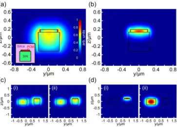
Figure 3. (a, b) Modal intensity profiles of a SiN waveguide loaded with a GSST strip in the (a) amorphous and (b) crystalline states. The inset in (a) illustrates the waveguide cross-section. (c) Intensity profiles of (i) even and (ii) odd supermodes in a two-waveguide system, one of which is topped with GSST while the other is not. The GSST layer is in: (c) the amorphous state; and (d) the crystalline state. All modes are TE-polarized. (a-d) Reproduced from [15]. Copyright 2018, Optical Society of America.
Fig. 3a and 3b illustrate the mode profile modification in a GSST-loaded silicon nitride waveguide. In the crystalline phase, GSST has sufficiently high index and the c-GSST itself can support a highly confined mode (Fig. 3b) with a large effective index of 2.28 + 0.30i, whereas the mode in Fig. 3a spreads across both a-GSST and SiN with a reduced effective index of 1.68 + (2.1 × 10⁻⁵)i. Clearly, the large modal modification cannot be accounted for using the classical perturbation theory.
Such a GSST-loaded waveguide is used here as a basic component to construct switching devices. The basic design rationale is to engineer the light propagation to allow input light to pass through GSST when it is in the low-loss amorphous state, and divert light away from the lossy c-GSST leveraging the large mode modification induced by the phase transition. As an example, Figs. 3c and 3d plot the supermode profiles of two juxtaposed waveguides, a GSST-loaded SiN waveguide and a SiN waveguide without GSST. The waveguide widths are adjusted such that their effective indices are identical when GSST is at amorphous state. Hence phase matching leads to strong coupling between the two waveguides with well-defined supermodes (Fig. 3c). In contrast, the large effective index difference between the two guides in the crystalline state results in two isolated modes (Fig. 3d).
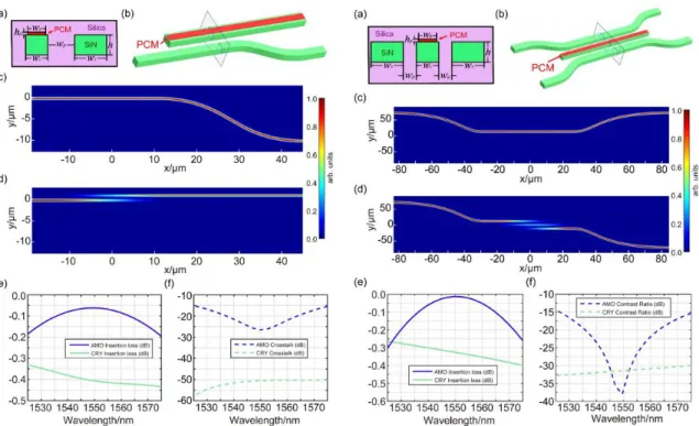
Figures 4a and 4b sketches a 1 × 2 switch assuming a directional coupler (DC) geometry based on the aforementioned two-waveguide system. When GSST is amorphous, the phase matching condition between the two waveguides is met. Light launched into the input waveguide is therefore coupled and efficiently transferred into the second waveguide. The low material attenuation in a-GSST ensures low-loss operation. On the other hand, when the GSST film is crystalline, input light almost exclusively couples into the mode shown in Fig. 3d (ii) and remains in the input waveguide. The minimal optical field interaction with the lossy c-GSST layer ensures low insertion loss. The simulated insertion loss (IL) and crosstalk (CT, i.e. contrast ratio between the on/off states at the output ports) are plotted in Figs. 5e and 5f. At 1550 nm,
Proc. of SPIE Vol. 11081 110811S-3
the device attains an IL of 0.4 dB and a CT of over -50 dB for the crystalline state, and an IL as low as 0.06 dB and a CT of -27 dB in the amorphous state.
Figure 4. (a, b) Schematics of the proposed 1 × 2 DC switches at (a) amorphous and (b) crystalline states.
Figure 5&6. (a, b) Cross section and 3D schematics of the waveguide structures. (c, d) Optical intensity distributions. (e, f) Insertion loss and crosstalk of the designed 1 × 2 and 2 × 2 photonic switches. Reproduced from [15]. Copyright 2018, Optical Society of America.
The “non-perturbative” design can be readily extended to 2 × 2 switches. Fig. 6a and 6b schematically depict the switch layout and Fig. 6c-f demonstrate the simulated field profile and device performance of the 2 × 2 DC switch. Although similar three-waveguide DC designs have previously been proposed14, 16-17, they were based on traditional GST. The high
loss at both states means GST material is unable to exploit the advantages of the non-perturbative design. To further illustrate this concept, in table 1, we modeled switches based on GST alloy as well as a traditional MZI design to elucidate the respective contributions to the device performance from 1) substitution of GST with GSST and 2) the non-perturbative
Table 1. Performance comparison between different 2 × 2 switch designs Traditional MZI Non-perturbative design GST GSST GST GSST IL (dB) 8.6 3.5 0.8 (1**) 0.2 CT (dB) 0.1 6.1 20 (15**) 32
design. In the MZIs, one of the interferometer arms is loaded with a thin layer of O-PCM to induce phase shift upon crystallization. The power splitting ratios in the arms are chosen to balance MZI arms when the O-PCM is in the amorphous state, which maximizes the CT. However, when the O-PCM is crystallized, its increased absorption results in power imbalance between the arms, compromising both the CT and IL. It can be shown that performance of MZI switches is defined by the classical FOM6, 18. On the other hand, with non-perturbative design, although device performance is
enhanced with lossy GST materials (**: experimental results demonstrated in reference [14], showing good agreement with the calculated result), the higher loss at amorphous state still limits the overall IL and CT compared with GSST. Results in Table 1, which indicate that only the combination of the GSST material and the non-perturbative design reaches the performance target, highlight the critical importance of both material innovation and device engineering.
3. SUMMARY
In this work, we demonstrate a design principle for non-volatile optical switches specifically designed for low-loss O-PCMs. Through combining our recent developed low-loss phase change alloy GSST and this non-perturbative design, the switches demonstrate significantly enhanced performances compared to current state-of-the-art. Across the telecom C-band, individual 1 × 2 and 2 × 2 switches exhibit ILs between 0.01 to 0.4 dB, and CTs consistently above 15 dB (> 25 dB at 1550 nm). We show that both the low-loss material property and the non- perturbative design are essential for achieving the exceptional device performance. The low-loss, non-volatile switching technology, once mature, will find numerous applications such as optical communications, signal processing, and field-programmable reconfigurable photonics.
ACKNOWLEDGEMENTS
DISTRIBUTION STATEMENT A. Approved for public release. Distribution is unlimited.
This material is based upon work supported by the Assistant Secretary of Defense for Research and Engineering under Air Force Contract No. FA8702-15-D-0001. Any opinions, findings, conclusions or recommendations expressed in this material are those of the author(s) and do not necessarily reflect the views of the Assistant Secretary of Defense for Research and Engineering.
© 2019 Massachusetts Institute of Technology
Delivered to the U.S. Government with Unlimited Rights, as defined in DFARS Part 252.227-7013 or 7014 (Feb 2014). Notwithstanding any copyright notice, U.S. Government rights in this work are defined by DFARS 252.227-7013 or DFARS 252.227-7014 as detailed above. Use of this work other than as specifically authorized by the U.S. Government may violate any copyrights that exist in this work.
This material is based upon work supported by the Assistant Secretary of Defense for Research and Engineering under Air Force Contract No. FA8721-05-C-0002 and/or FA8702-15-D-0001, and by the Defense Advanced Research Projects Agency Defense Sciences Office (DSO) Program: he Young Faculty Award Program under Grant Number D18AP00070 and the EXTREME Optics and Imaging (EXTREME) under Agreement No. HR00111720029. The authors also acknowledge characterization facility support provided by the Materials Research Laboratory at MIT, as well as fabrication facility support by the Microsystems Technology Laboratories at MIT and Harvard University Center for Nanoscale Systems. The views, opinions and/or findings expressed are those of the authors and should not be interpreted as representing the official views or policies of the Department of Defense or the U.S. Government.
REFERENCES
[1] Yin, X., Steinle, T., Huang, L., Taubner, T., Wuttig, M., Zentgraf, T., & Giessen, H, “Beam switching and bifocal zoom lensing using active plasmonic metasurfaces,” Light: Science & Applications, 6, e17016 (2017).
[2] Li, P., Yang, X., Maß, T.W., Hanss, J., Lewin, M., Michel, A.K.U., Wuttig, M. and Taubner, T., “Reversible optical switching of highly confined phonon–polaritons with an ultrathin phase-change material,” Nature materials, 15, 870-875 (2016).
[3] A.-K. U. Michel, D. N. Chigrin, T. W. Maß, K. Schönauer, M. Salinga, M. Wuttig, and T. Taubner, "Using low-loss phase-change materials for mid-infrared antenna resonance tuning," Nano Lett. 13, 3470-3475 (2013).
[4] C. Ríos, M. Stegmaier, P. Hosseini, D. Wang, T. Scherer, C. D. Wright, H. Bhaskaran, and W. H. Pernice, "Integrated all-photonic non-volatile multi-level memory," Nat. Photonics 9, 725-732 (2015).
Proc. of SPIE Vol. 11081 110811S-5
[5] P. Hosseini, C. D. Wright, and H. Bhaskaran, "An optoelectronic framework enabled by low-dimensional phase-change films," Nature 511, 206-211 (2014).
[6] X. Y. Sun, Q. Du, T. Goto, M. C. Onbasli, D. H. Kim, N. M. Aimon, J. Hu, and C. A. Ross, "Single-step deposition of cerium-substituted yttrium iron garnet for monolithic on-chip optical isolation," ACS Photonics 2, 856-863 (2015). [7] M. Rudé, J. Pello, R. E. Simpson, J. Osmond, G. Roelkens, J. J. van der Tol, and V. Pruneri, "Optical switching at
1.55 μm in silicon racetrack resonators using phase change materials," Appl. Phys. Lett. 103, 141119 (2013)
[8] M. Stegmaier, C. Ríos, H. Bhaskaran, C. D. Wright, and W. H. Pernice, "Nonvolatile All‐Optical 1× 2 Switch for Chipscale Photonic Networks," Adv. Opt. Mater., 5, 1600346 (2017).
[9] Y. Zhang, J. Li, J. Chou, Z. Fang, A. Yadav, H. Lin, Q. Du, J. Michon, Z. Han, Y. Huang, H. Zheng, T. Gu, V. Liberman, K. Richardson, and J. Hu, "Broadband Transparent Optical Phase Change Materials," in Conference on Lasers and Electro-Optics, paper JTh5C.4 (2017).
[10] Y. Zhang, J. B. Chou, J. Li, H. Li, Q. Du, A. Yadav, S. Zhou, M. Y. Shalaginov, Z. Fang, H. Zhong, C. Roberts, P. Robinson, B. Bohlin, C. Ríos, H. Lin, M. Kang, T. Gu, J. Warner, V. Liberman, K. Richardson and J. Hu, "Extreme Broadband Transparent Optical Phase Change Materials for High-Performance Nonvolatile Photonics," arXiv preprint arXiv: 1811.00526 (2018).
[11] C. Wu, H. Yu, H. Li, X. Zhang, I. Takeuchi, and M. Li, “Low-Loss Integrated Photonic Switch Using Subwavelength Patterned Phase Change Material,” ACS Photonics 6(1), 87–92 (2019).
[12] Zhang, H., Zhou, L., Lu, L., Xu, J., Wang, N., Hu, H., Rahman, B.A., Zhou, Z. and Chen, J., “Miniature Multi-Level Optical Memristive Switch Using Phase Change Material,” ACS Photonics (2019).
[13] Zhang, H., Zhou, L., Xu, J., Wang, N., Hu, H., Lu, L., Rahman, B.M.A. and Chen, J., “Nonvolatile waveguide transmission tuning with electrically-driven ultra-small GST phase-change material,” Science Bulletin, 64(11), 782-789 (2019).
[14] Xu, P., Zheng, J., Doylend, J.K. and Majumdar, A., “Low-loss and broadband nonvolatile phase-change directional coupler switches,” ACS Photonics, 6(2), 553-557 (2019).
[15] Q. Zhang, Y. Zhang, J. Li, R. Soref, T. Gu, J. Hu, "Broadband Nonvolatile Photonic Switching Based on Optical Phase Change Materials: Beyond the Classical Figure of-Merit," Optics Letts., 43, 94-97 (2018).
[16] Y. Ikuma, T. Saiki, and H. Tsuda, IEICE Electronics Express 5, 442-445 (2008).
[17] H. Liang, R. Soref, J. Mu, A. Majumdar, X. Li, and W.-P. Huang, J. Lightwave Technol. 33, 1805-1813 (2015). [18] R. A. Soref, D. McDaniel, and B. R. Bennett, J. Lightwave Technol. 6, 437-444 (1988).