Development of Gallium Nitride Power Transistors
Daniel Piedra
S.B., Electrical Engineering M.I.T., 2009
Submitted to the Department of Electrical Engineering and Computer Science in Partial Fulfillment of the Requirements for the Degree of
Master of Engineering in Electrical Engineering and Computer Science
ARCHrVES
at the Massachusetts Institute of TechnologyMASSCHUE-TTS
INSTITUTE1
OF TECH
November 2010
Efebr
.
?0v)I
JUN 2 1
2011
Copyright 2010 Daniel Piedra. All rights reserved.
LIBRA
RIES
The author hereby grants to M.I.T. permission to reproduce and
to distribute publicly paper and electronic copies of this thesis document in whole and in part in any medium now known or hereafter created.
Author
Department of Electrical Engineering and Computer Science November 24, 2010 Certified by
Accepted by
Tomis Palacios Emmanuel E. Landsman Associate Professor Thesis Supervisor
Dr. Christopher J. Terman Chairman, Department Committee on Graduate Theses
Development of Gallium Nitride Power Transistors by
Daniel Piedra Submitted to the
Department of Electrical Engineering and Computer Science November 24, 2010
In Partial Fulfillment of the Requirements for the Degree of Master of Engineering in Electrical Engineering and Computer Science
ABSTRACT
GaN-based high-voltage transistors have outstanding properties for the development of ultra-high efficiency and compact power electronics. This thesis describes a new process technology for the fabrication of GaN power devices optimized for their use in efficient power distribution systems in computer micro-processors. An existing process flow was used to
fabricate the baseline single-finger transistors and additional process steps were developed and optimized to fabricate multi-finger devices with total gate widths up to 12mm. These transistors offer the current and on-resistance levels required by future GaN-based power converters. Transistors with various gate widths were fabricated and characterized by DC and capacitance-voltage measurements to study how the main transistor metrics scale with gate width.
Acknowledgements
I would like to thank my advisor Professor Tomais Palacios for all of his help and
guidance over the course of this MEng thesis and further back to my days as a UROP. I am very grateful for all of his advice and his assistance in striving to be a great researcher.
I would also like to thank my fellow students in the group. Bin Lu, Omair Saadat, Feng Gao, Allen Hsu, Dr. Mohamed Azize, Will Chung, Han Wang, Dong Suep Lee, Kevin Ryu, and Benjamin Mailly have all provided great insight in and out of the clean room. Elizabeth Kubicki has always been very helpful in assisting with ordering necessary materials.
I would like to thank the MTL staff for training and assistance with the clean room tools. None of this would have been possible without the support of my family, for which I am very grateful.
Table of Contents
C hapter 1: Introduction... .5
Section 1.1: Introduction to Power Electronics... 5
Section1.2: Gallium Nitride for Power Devices... 8
Section 1.3: Application- Power Regulation and Distribution in Microprocessors...12
Section 1.4: Project Goals...14
Chapter 2: Fabrication of GaN Multi-finger Transistors...15
Section 2.1: Motivation for Multi-finger Technology...15
Section 2.2: Design of GaN Power Devices...16
Section 2.3: GaN High Electron Mobility Transistor (HEMT)...20
Section 2.4: Multi-finger Process...27
Chapter 3: Device Characterization...36
Section 3.1: Direct Current IV Measurements...36
Section 3.2: Capacitance Measurements...-49
Section 3.3: Theoretical Parameter Calculations...53
Section 3.4: Summary of Device Metrics...56
Chapter 4: Conclusion and Future Work...60
Appendix A: Process Flow... .. ... 66
Chapter 1: Introduction
Section 1.1: Introduction to Power Electronics
Power electronics have become a substantial part of the semiconductor business. About ten percent of the semiconductor industry's 200 billion dollars of revenue come from power integrated circuits and power semiconductor devices. An estimated 50% of the electricity used in the world is controlled by power devices [1]. Since they have become such an integral component of the modem world, it is very important that the power semiconductor devices are very efficient. The performance of the device ultimately dictates the efficiency of the system.
Furthermore, size and cost will determine the success of future power systems, so it is important to develop compact, economical solutions.
Power electronics is concerned with the control and conversion of electrical power using semiconductor switches. Applications of power electronics are widespread and encompass systems operating over a broad range of power levels, frequencies, voltage ratings and current ratings as shown in figures 1 and 2. In homes and offices, 60 Hz alternating current is converted to direct current for use in electronics such as computers and televisions [2]. Hybrid vehicles require conversion from DC from their batteries to AC to run their motors [3]. Solid state lighting requires power electronic down converters to reduce the 11 OV supplied voltage to the much lower voltage required by the light emitting diodes (LEDs). On the very high end of the voltage spectrum, voltages greater than 10kV are used in grid applications. Large transformers
are used to step down voltages from hundreds of thousands of volts on the transmission grid to thousands of volts on the distribution grid.
-lot
cetIuU.TVcomm EATWO G
mizcvoweva oveP
System Operating Fregqeney (Hi)
Figure 1. Applications for Power Electronics [1] IVV ELECTRIC "To RAIN
t:02
DRIVES
ROBOTC3 II 10*' 10 10o 10 10'Voltage Rating (Volts)
Figure 2. Voltage and Current ratings for power electronic systems [1]
One fundamental application of power electronics is DC to DC down conversion, where the output voltage is a fraction of the input voltage. This conversion scheme is widely used in electronic systems such as cellular phones, hybrid automobiles, and laptop computers which are comprised of several circuits that have lower voltage requirements than the battery supplies. For
this task, a circuit such as the one shown in figure 3 is used [4]. By controlling the switches in a periodic fashion (periodic waveform shown in figure 4), the output voltage can be "stepped down" to a fraction of the input voltage.
Si VS L S2 Vout Rload il
Figure 3. Basic step-down DC-DC converter.
V
hA
TOFF
TONVOUT
t Figure 4. Load voltage waveform
During the time period TON, the switch SI is closed and the switch S2 is open, thus giving the
following expression for the voltage in the circuit:
dii(t) Vs = Ri1 (t)+ L dt
During the time period TOFF, the switch Si is open and S2 is closed, causing the load voltage to
become zero:
dii (t)
0 = Ri1(t)+ L dt
At the completion of TOFF, SI is closed and the cycle begins again. Thus the cycle time (and inverse fundamental frequency) is:
1
T
= TON + TOFFThe average voltage at the output is
TTON
T
Vout=4jVs dt +
0
0dt =Vs TON= VsT fON =ONV.t=T f f T 4T~ STON +TOFF V
0 TON
It is shown that by controlling the ratio , called the duty ratio D, the output voltage can be T
"stepped down" to a specific fraction of the input voltage. This is the basic concept employed by down converters. Operation of the circuit and thus control of the output voltage is ultimately dependent on the switches S1 and S2. In the early part of the 2 0th century, these switches were
vacuum tubes, but have since then have been replaced by solid-state devices.
Section 1.2: Gallium Nitride for Power Devices
After the replacement of vacuum tubes by solid-state devices, silicon based semiconductor power devices have been dominant [1]. Considering the wide use of the switching devices, improvements are being sought. The relatively low breakdown voltage of silicon, low operating temperatures, and its high resistance open the door for a viable
replacement material. A new switching technology that would improve the switching frequency, on-resistance, and maximum temperature is desirable, since these are important metrics of the
switch.
Nitride semiconductors have the material characteristics to fabricate devices that would make an improved switching technology possible. The nitride family of semiconductors span a
very large bandgap range, from 0.6eV in InN to 3.4eV in GaN to 6.2eV in AIN and are well suited for many applications. In particular, gallium nitride has outstanding properties for power electronics. Originally used in optoelectronic devices, GaN has a wide bandgap, giving it a high breakdown voltage. GaN and other wide band semiconductors have the characteristic of small
lattice constants, so the distance between unit cells in the crystal lattice of the material is smaller than in Si. The small lattice constant results in a strong atomic bond and thus high stability with almost 10 times improvement in critical electric field [5]. Furthermore, GaN can form
heterojunctions (interfaces between materials with different bandgaps), so this semiconductor can be used in the fabrication of high electron mobility transistors (HEMTs). In HEMTs, there is a thin layer of highly mobile electrons in the channel, known as the two-dimensional electron gas (2-DEG). HEMTs have higher carrier concentrations and electron mobility than traditional transistors and are thus desirable for many applications, including power electronics (Table 1).
Figure 5. Diagram of an AlGaN/GaN HEMT (High Electron Mobility Transistor)
Table 1. Comparison of material properties of Si, GaN, and SiC [6]
Si GaN 4H-SiC
Band Gap Eg (eV) 1.1 3.39 3.26
Breakdown Electric 0.3 3.3 3.0
Field Eb, (MV/cm)
Peak drift velocity vsat 1.0 2.5 2.0
(107 cm/s)
Electron mobility p, 1350 2000 (2 dimensional 700 (cm2
/Vs) electron gas)
Relative dielectric 11.8 9.0 10
constant c
Johnson Figure of Merit 1 27.5 20
(Ebr vsat/2n)
Baliga's Figure of Merit 1 1507 548
(e Ec3)
Low on-resistance is an important characteristic for transistors used in power applications, because this will determine the power dissipated. This dissipated power is
comprised of conductive power loss and switching power loss. The switching waveform shown in figure 4 exists only for ideal power switches that have on state resistance of zero. For such a device, there is no power dissipation in the transition states from on to off. Unfortunately, real power switches have some on-resistance, so the transition from on to off is not instantaneous, resulting in the waveform shown in figure 5. Devices with large on-resistance deviate greatly from the ideal power switching device and thus have more dissipated power.
TOFF TON
+- +-+ VoUr
/
t
In general, the on-resistance in transistor devices is given by [I]:
4 4V2
Ron = sn
The inverse dependence on mobility and breakdown field favors a semiconductor with high electron mobility and high breakdown field to minimize on-resistance. As seen in table 1, GaN is superior to silicon in both these respects. Figure 7 shows on-resistance as a function of breakdown voltage for GaN, Si, and SiC.
100
10 L
10
10 10 10 3 10 4Figure 7. On-resistance as a function of breakdown voltage for switching applications [9]
Currently, GaN is grown on substrates of Si, SiC, or sapphire, as there is not yet an inexpensive method to make GaN substrates. Factors such as crystal lattice uniformity, heat conduction and cost are important in the selection of the substrate. Gallium nitride grown on silicon carbide has shown good performance due to the fact that the two compounds are well crystal lattice matched. However, GaN on SiC is very expensive, with a 100mm wafer costing up to $10,000 [3]. A more cost appealing alternative is GaN grown on Si, so this thesis is
focused on this method. Advancement of this technology is important, since gallium nitride power switches are being pursued for use in hybrid vehicles, power adapters, and power regulation systems in microprocessors.
Section 1.3: Application: Power regulation and distribution in microprocessors
In current microprocessors, low voltages are needed to reduce the energy consumption during switching. However, the low voltages at which the power is distributed limit the circuit performance and significantly increase power dissipation due to ohmic losses.
.. Pont _IVout _ n - J R _ JR
Eff iciency - -- - - -
1-Pin n iin n
Thus, high efficiency power transmission requires high Vi, and low current. Such a power transmission method is employed in power lines. Power is transmitted at a high voltage, low current to maximize efficiency and then the voltage is stepped down to the necessary voltage levels when needed. However, this is difficult with conventional silicon devices, which cannot simultaneously take high Vin and high switching frequencies due to their relatively low critical electric field. Off chip regulators are needed in this case. This causes a waste of space and input lines into the microprocessor to introduce current at the stepped down voltage. It would be more efficient to have on chip regulators. Such devices must have low on-resistance and operate at a high switching frequency and high voltage. Furthermore, the devices must be integrated with silicon chips to take advantage of the existing silicon processing infrastructure. The high switching capabilities of GaN power transistors enable the possibility of on chip converters for local conversion from 12V to low voltage (approximately 1V).
L
- C
VV.
MAIFigure 8. Step down DC to DC converter in integrated GaN/Si system. DI and DI' are GaN transistors. D2 and D2' are Si transistors.
Microprocessor Die
Regulation Node
Source: M. Budnik, 2006
Figure 9. Proposed power distribution system in microprocessor[7]
Section 1.4: Project Goals
Power switches need to have low on-resistance to minimize dissipated power losses. At the same time, the switches need to have high breakdown voltage so that they can withstand unexpected voltage spikes and a low gate capacitance for high switching operation, which requires a small transistor footprint. The goal of this project is to develop a fabrication
technology for GaN power switches that will meet these requirements. Furthermore, this project will investigate how important transistor metrics scale with device dimensions. Specifically, the multi-finger process technology developed in this project will be used to fabricate transistors with very long gate widths to examine how maximum drain current, gate leakage current, on-resistance, and gate capacitance scale with increasing gate width.
Chapter 2: Fabrication of Multi-finger Transistors
Section 2.1: Motivation for Multi-finger Technology
Large amounts of current flow through the power devices required in computer power supplies, the main application space in this thesis. To accommodate such a high current level, large transistors with very long gate widths (on the order of tens to hundreds of millimeters) are necessary.
However, transistors of such a large size, while ideal for high voltage situations, represent an obvious departure from the typical dimensions used in GaN transistors for RF amplifier applications. Circuits composed of several of these twenty-millimeter gate width transistors would be massive compared to circuits built with the 150-micron gate width counterparts. Furthermore, the gate resistance present in such a large transistor would degrade the frequency performance of the device. The ideal power transistor would combine the best of both worlds and fit a large gate width into a microscopic package. Multi-finger transistor technology could be used to fabricate micron scale gallium nitride transistors that have the advantages of long gate widths. The essence of the idea is to fabricate a linear structure with alternating separate
source/drain pads. A single gate is intertwined between the separate source and drain pads, giving a structure resembling traditional transistors. This approach provides the long gate width required for power electronics, but since the gate is intertwined between the separate sources and
drains (rather than laid out in a single straight line), space will be conserved. The completed multi-finger devices will have the equivalent gate width of much larger devices, but occupy a smaller area, as seen in figure 10.
... Drin < . Gate 300 pmn
41Multi-finger
technology Gate 50 ur y L Source'Figure 10. The Advantage of Multi-finger devices. In the figure above, the transistors have the same gate width, but the multi-finger device is more compact (6 fingers of 50pim each)
Section 2.2: Design of GaN Power Devices
To fabricate the GaN power transistors, a new photolithography mask design was developed. The new mask had conventional single-finger devices, as seen in figure 11. Single-finger devices were included in the mask to test device quality prior to any multi-Single-finger specific processing steps. Furthermore, the transistor metrics of these devices with a Wg of only 100pm were compared against the multi-finger devices with larger gate width to examine the effects of increasing gate width.
4- Gate Mesa Isolation
--- i
Drain Source
Figure 11. Single-finger transistor. WgJ=100gm, Lgd=10 rn, Lgs= 1.5 pim,
Lg=2 gm
Additionally, the mask included multi-finger devices. A multi-finger device on this mask is comprised of several Wg=3 0 0 pm single-finger devices with shared source, drain, and gate contacts. The total gate width of the multi-finger device can vary depending on how many single-finger devices are tied together. Figures 12 and 13 illustrate how the complete Wg=12 mm device is composed of smaller two Wg=6 mm devices, which are each composed of twenty Wg=3 0 0 pim devices. Prior to any multi-finger processing, individual Wg=300 Im devices can be measured. A dielectric is deposited and openings are etched to give access to the source contact. A metal stack is deposited across the opening to connect each single-finger device. Connecting the devices on the top half (but keeping them isolated from the bottom half) give a Wg 6 mm device. Finally connecting the top and bottom half give the complete Wg=12 mm device.
Top half, which has 20 single-finger devices Bottom half, which has 20 single-finger devices Zoomed in view showing individual gate fingers Single-finger, Wg=300pm device So rce Gate Complete multi-finger device, which has 40 single-finger devices Drin
Figure 12. Prior to any multi-finger processing steps, this structure is 40 individual single-finger transistors
Connect top half single-finger devices with metal bridges Top half, which is a
W=6mm device
Bottom half, which is a W=6mm device
4
4;
Complete deviceWg=12mm device
Connect top and bottom halves with metal
4
Figure 13. The complete Wg=1I 2mm multi-finger device is composed of two Wg=6mm, which are each composed of twenty Wg=300pm devices
Connect bottom half single-finger devices with metal bridges
Section 2.3: Standard GaN High Electron Mobility Transistor (HEMT)
This chapter describes the process used to fabricate multifinger GaN High Electron Mobility Transistors. The devices were fabricated on AlGaN/GaN structures grown on Si (111) by Metalorganic Chemical Vapor Deposition (MOCVD). The AlGaN layer had an Al
composition of 26% and a thickness of 17nm. The sheet resistance of the material was 439Q/sq, as determined by TLM characterization.
AIGaN 17nm
2DEG Rsheet=4390/sq
GaN Si Substrate
Figure 14. AlGaN/GaN on Si wafer. The AlGaN/GaN heterostructure causes 2-dimensional electron gas.
In preparation for processing, the piece was cleaned with acetone, isopropyl alcohol, and deionized water and baked on a hot plate at 1300 C to evaporate all solvents.
First, mesa isolation was performed by electron cyclotron resonance (ECR) etching to electrically segregate the devices from one another. The principle is to etch away the AlGaN layer to the GaN layers, so that the heterojunction (where 2-dimensional electron gas exists) is removed and there is not unwanted current between devices. The mesa pattern was defined by spinning on OCG-825 photoresist, prebaking to cure the resist, exposing in the Karl Suss MA-6 aligner, and developing in OCG934 solution. After patterning, the sample underwent etching with the following parameters:
Table 2: Mesa Isolation Etch Parameters
photoresist
Figure 15. Mesa Isolation. After etching, area not protected by photoresist is etched away creating electrical isolation between devices by cutting off the 2DEG
Figure 16. Top view of mesa Isolation pattern in a multi-finger transistor
Step 1 Step 2 Step3 Step 4 Step 5 Step 6
BC13 (sCcm) 10 10 10 20 20 20 C12 (sCcm) 0 0 0 5 5 5 Pressure (mTorr) 10 10 10 10 10 10 ECR (W) 0 50 100 0 50 100 RF (W) 0 15 15 0 15 25 Time (s) 30 5 60 30 5 400
Mesa isolation was done first to avoid photoresist problems caused by plasma etching. Plasma in the etcher made the OCG-825 resist insoluble to acetone, and thus very difficult to remove. Neither acetone nor heated N-Methyl-2-pyrrolidone (NMP) provided a reliable method of removing resist. Exposure to oxygen plasma for 15 minutes successfully removed the
photoresist from the sample. However, prolonged time periods in oxygen plasma damaged any metal resulting in poor device performance. Performing mesa isolation first gives the freedom to expose to oxygen plasma since there is not yet any deposited metal on the sample.
The next step in the process was the patterning and deposition of ohmic contacts. The contacts were patterned by spin coating AZ5214 image reversal photoresist on the sample and prebaking at 80'C on a hotplate to cure the resist. An initial 8 second exposure (with the ohmic contacts mask) established the pattern on the sample and a 1100 C reversal bake crosslinks the
exposed areas of photoresist, making those areas inert to developer. The sample then underwent an 80 second flood exposure (without a mask), which makes all areas that are not crosslinked soluble to developer. The sample was then agitated in AZ422 developer to dissolve all soluble areas of photoresist (where ohmic contact metal will ultimately be). The metal stack of 200A Ti, 1000
A
Al, 250A Ni, 500A
Au was deposited by electron beam evaporation. The sample was then placed in acetone to dissolve the underlying photoresist and liftoff the metal in all areas around the contact areas.-Au
Al
photores ist
-AIGa N
Figure 17. Liftoff of ohmic contact metals. The e-beam evaporation deposits a uniform layer of metal on the entire sample. Photoresist dissolves in acetone, lifting off metals in the regions around the contacts. Figure is not drawn to scale.
Source
Figure 18.Ohmic contact pattern seen from above view
The sample then underwent a rapid thermal anneal at 870'C for 30 seconds in a nitrogen atmosphere. High temperature annealing caused the metal alloy to vertically diffuse into the Ni
surface. The sample was then cleaned with acetone, isopropyl, deionized water and baked at 130' C to evaporate solvents. The resulting ohmic contacts had a contact resistance of 285Qmm, as determined by TLM characterization.
S D
AIGaN
2DEG
GaN
Figure 19. Rapid Thermal Annealing. During annealing, there is diffusion of ohmic metals to make contact with 2-Dimensional electron gas
Figure 20. Micrograph of annealed ohmic contacts
Next, a 17nm layer of aluminum oxide was deposited on the sample by atomic layer deposition (ALD) to serve as a gate dielectric to minimize gate leakage current. The aluminum oxide layer also acts as a partial passivation layer. Contact pad openings were patterned using OCG825 photoresist and the aluminum oxide over these openings was etched by a dip in 7:1 buffered oxide etch (BOE) for 20 seconds.
After cleaning with acetone, isopropyl, and deionized water, the sample was ready for gate metal deposition. The same liftoff process described above was used. The gate pattern has much smaller features than the ohmic contact pattern, so it was important that the exposure time and reversal bake time and temperature were exact. Inspection under the fluoroscope was done to insure proper alignment and definition of the gate patterns. The sample was descummed in
the oxygen plasma asher for 5 minutes at 1000W. A schottky metal gate stack of
300A
Ni, 2000A Au, and 500A Ni was deposited by electron beam evaporation. Agitation in acetone dissolved the underlying photoresist and lifted off the metal in all areas around the gates.This concludes the process for fabricating standard GaN High Electon Mobility Transistors.
Figure 22.Gate metal pattern seen from above view
Figure 23. GaN transistors prior to multi-finger processing
Section 2.4: Multi-finger Process
The sample was cleaned with acetone, isopropyl, and deionized water and baked at 130'C to evaporate solvents to prepare the surface for coating. AP3000 solution was spun on the sample at 500rpm for 5 seconds to spread, then 2000rpm for 30 seconds. AP3000 is a silane based adhesion promoter which enhances the interfacial adhesion of BCB to inorganic surfaces, which is otherwise poor [8]. Next, BCB was dispensed on the sample and spun on at 500rpm for
5 seconds to spread, then 1500 rpm for 60 seconds for a target thickness of 2 microns. T 1100
rinse solution was lightly swabbed on the backside and edges of the piece to remove excessive BCB. The coated piece was prebaked at 1100 C to remove solvents and stabilize the film. The sample was then placed in an oven with nitrogen atmosphere at 250*C for one hour to cure the BCB.
At this point in the process, the entire sample was coated with BCB and openings had to be patterned and etched to access the metal contacts. Two different masking techniques were tested: a chromium hard mask and a photoresist soft mask.
AZ4620 thick photoresist was dispensed and spun at 1500rpm for 9 seconds to spread, 4000rpm for 60 seconds, and 5000rpm for 10 seconds to remove edge bead. The sample was
then placed in a pre-bake oven at 95*C for 10 minutes to cure the resist, exposed in the Karl Suss aligner, and developed in AZ400 to remove the photoresist above the areas that needed to be opened. The resist acted as a soft mask (sacrificial layer) in the etching process.
A chromium hard mask was deposited on another sample. A 750A layer of Cr deposited by electron beam evaporation and patterned by the same liftoff process described above.
Figure 24. Openings pattern shown in black, with underlying metals shown in
cross pattern.
Prior to etching the sample, work was cone to determine the etcn rate of BCB with a given etch chemistry and power. A dummy silicon piece was prepared by spinning on BCB as
described in the preceding paragraph. ECR etching was performed on the silicon dummy piece. The etch conditions are shown in the table below.
Table 3. BCB etch conditions
Step 1 Step 2 Step3
02 (sccm) 40 40 40 CF4 (sccm) 5 5 5 Pressure (mTorr) 10 10 10 ECR (W) 0 15 100 RF (W) 0 30 30 Time (s) 30 5 vary
The piece was etched for three different times and the thickness of the BCB layer after each etch was measured using a spectroscopic reflectometry tool, the Nanometrics Nanospec. The results are shown in figure 25 below. From this data, the etch rate of BCB in
0
2/CF4 wasextrapolated. With this etch rate, it was determined that 21 minutes of etching would remove the approximate 2 micron thick layer of BCB on the sample.
2.5 2 1.51 4.0 0.5 0 4-- -- '---- ---0 2 4 6 8 10 12 14
Etch time (min)
Figure 25. Etch rate of BCB in CF4/02 plasma =
0.096 micron/minute
The GaN samples with transistors were etched for the necessary time to remove the BCB not shielded by a masking material, thus creating openings to the metal contacts. Agitation in acetone removed the remaining photoresist on the sample with the soft mask, and a 30 second immersion in Cr etchant removed the remaining chromium on the sample with the hard mask.
M-. Cr Mask (700A thick) BCB AIGaN GaN Si 02/CF4 plasma etching BCB BCB BCB S S AIGaN GaN Si
Figure 26. BCB Etching. Areas above the source contacts not covered by masking material are etched.
Different results occurred from the different masks. Figures 27 and 28 below illustrate the differences. In these micrographs the source openings have been coated with gold (as required to connect the separate sources). The openings etched with photoresist mask had poor definition and uniformity. As seen in figure 27, the openings have a round shape and the features on the left of the figure are much more etch than the features on the right.
source openings
Figure 27. Etched source openings with photoresist mask.
source openings
-Figure 28. Etched source openings with Cr mask.
The differences in quality of etch definition of the openings can be explained by a
fabrication effect called the aspect ratio dependent etching (ARDE) lag. Variations in the size of the pattern opening will cause variations in the etch rate of the specific material. Specifically, larger features (having smaller depth to width aspect ratios) will etch faster than smaller features (having larger depth to width aspect ratios).
8pm Photoresist mask No
0 0"
small aspect ratio BCB large aspect ratio
Figure 29. Thicker masking layer results in blocking of etching species in the smaller openings. This results in a non-uniform etch
750A Cr mask -
-/0_0 0" 0--4
BCB
Figure 30. Thinner masking layer results in less blocking of etching species in the smaller openings. There is a small aspect ratio for all features, resulting in a uniform etch.
Etch resistance of Cr in BCB etch chemistry is much better and thus a thinner layer will suffice and there ARDE lag will not be as drastic, meaning that the piece can be etched more uniformly. It was thus decided that the thin Cr mask was the better option and subsequent
devices were processed using this hard mask.
O\
0,'Iep
O
T q T
Etched openings
-Figure 31. Micrograph of BCB etched piece
The next step in the process was the patterning and deposition of the bridge metals to connect the source contacts. The bridges were patterned by spin coating AZ5214 image reversal photoresist on the sample and prebaking at 80*C on a hotplate to cure the resist. The sample underwent an initial 8 second exposure (with mask) and was then baked at 110* C. The sample then underwent an 80 second flood exposure (without a mask) and was agitated in AZ422 developer. The metal stack of 500A Ti, 5000
A
Au, 550A Ni was deposited by electron beam evaporation. The sample was then placed in acetone to dissolve the underlying photoresist and liftoff the metal in all areas around the contact areas.r:1'[:Yri'I'1"T[
is
171'
:YiYIYIYI;1'Y: YIYI1
Figure 32. Deposited metal shown in the diagonal lined pattern and the openings to BCB shown in black.
4-500A Ti, 5000A Au, 500A Ni
BCB BCB BCB
SD
Fd
S
N
AIGaN GaN
Si
Figure 33. Metallization to connect the source pads
Figure 34. Multi-finger transistor.
Devices fabricated up to this step underwent initial IV characterization, but the transistors exhibited a problem at drain voltages of about 9V- 1 OV and drain currents approaching 1A. Dark spots appeared in the drain contact (as seen in figure 35) and the drain current was greatly reduced. To correct this problem, associated with the high resistance of a relatively thin metal layer, an additional layer of metal (200A Ti, IkA Au) was deposited on the contact pads and patterned by the liftoff technique described above.
Chapter 3: Device Characterization
This chapter describes the device characterization procedures and results from the fabricated devices described above. Direct current-voltage (IV) and capacitance measurements were taken from several devices varying in gate width (other dimensions constant) to study how several device parameters scale.
Section 3.1: Direct Current IV Measurements
Measurements of Ids-Vds characteristics were taken using an Agilent 4155C
Semiconductor Parameter Analyzer. This parameter analyzer is constrained by a built-in current compliance limit of 1OOmA, so it was used in conjunction with the Agilent 41501B SMU and Pulse Generator Expander to get the current compliance limit up to 1A.
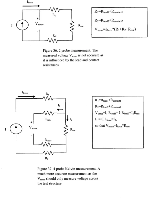
For the large current anticipated from these devices, it was expected that the probe resistances would not be negligible. To limit the effect of the probe resistances, the 4-probe
Kelvin measurement technique was used [10]. For this type of measurement, two of the probes are dedicated to source and sink current, while the other two are used to measure voltage. The probes being used to measure voltage draw no current and thus there is no resistive voltage drop in the measurement lines to invalidate the voltage measurement. Figure 37 illustrates this concept.
Iforce
Figure 36. 2 probe measurement. The measured voltage Vsense is not accurate as
it is influenced by the lead and contact resistances
force
Figure 37. 4 probe Kelvin measurement. A much more accurate measurement as the Vsense should only measure voltage across the test structure.
Ri-=Rica I +Rcontactl
R2=Rea2+Rcontact2
Vsense-force*(RI +R2+Rest)
Ri=Rlead1+Rcontacti
R2=Rea2+Rcontact2
Vsense= I Read3+ II Rleac3+I2Rest
I = 0, Iforce=I2,
Figure 38 is an optical micrograph showing how the 4-probe Kelvin measurement method was used on the multi-finger GaN devices fabricated in this thesis.
Drain
Probe 5 (gate)
I
Source
Figure 38. Probe 1 was set to ground, probe 2 was set to have variable voltage, and Id was I2. Defined Vds as V3-V4, so probes 3 and 4 drive no current, they only measure the voltage difference
Using the 4-probe Kelvin measurement, the following IV measurements were taken:
Wg=100pm, Lg=2Am, Ldg=10pm, L,g=1.5m
Wg=100Lm, Ldg=10Lm
0 1 2 3 4 5 6 7 8 9 10
vdgv)
Figure 39. Id-Vds characteristics of device
with gate width of 100pLm. Idmax = .056A
y = 0.01 24x + 4E-05
V=1V
AId slope = LXVds 0.2 0.4 0.6 0.8 VdS(V)Figure 40. Close up segment of Id-Vds curve, illustrating the on-resistance, slope=0.0124A/V
0.014 0.012 0.01 0.008 0.006 0.00 0.0c -0.0c 1
Row
4 2 2The slope of the line in figure 40 represents the change in Id over the change in Vds in the linear (triode) region. This slope is the inverse of the resistance times the gate width. Thus, the on-resistance, Ron, is calculated by taking the inverse of the slope of the line times the gate width
1 _ 1 R = * * .100mm = 80.6fl * .100mm = 8.060mm slope 0.0124A/V
1E-12
1-
-1E-13 tAo AE1 A AA A Vds(V)Figure 41 .Ig-Vds (gate leakage current) measurements (Vg=IV to -6).
Wg=300pm, Lg=2pm, Ldg=10pm, Lg=1.5pm
Wg=3 00 [Lm, L,,=10 [m
0.14 , 9 1 1
0 1 2 3 4 5 6 7 8 9 10
VdSM
Figure 42. Id-Vds characteristics of device with gate width of 3001pm. Idmax =. 127A
0.02 0.015 0.01 0.005 0 -0.005 V =1V AMd 1 slope= - =-W 0Vds 1.2 0.2 0.4 0.6 0.8 1 1.2 VdS (V)
Figure 43. Close up segment of Id-Vds curve, illustrating the on-resistance, slope=.O1 89A/V
1
= * .300mm = 52.9il * .300mm = 15.87f2mm
0.0189A/V
=o 1 *
0.01 0.0001 0.000001 1E-08 0 2 4 6 8 10 12 - - - -- - - - - -_ _ _ _
4--1E-10 1E-12 1E-14 Vds(V)Figure 44. Ig-Vds (gate leakage current) measurements (Vg=1V to -6). Igmax=1.48x10-A Wg=600micron, Lg=2pm, Ldg=10pm, Lg=1.5gm W =600pm, Ldg=lP0fL 5 VdSM
Figure 45. Id-Vds characteristics of device with gate width of 600pm. Idmax= .260A
-0.04 -0.035 - y =0.0353x + 2E-05 0.03 - V =1V 0.025 -0.02 - AM 1 slope = XVds 0.015 -0.01 0.005 0 0.2 0.4 0.6 0.8 1 1.2 -0.005 VdSM
Figure 46. Close up segment of Id-Vds curve, illustrating the on-resistance, slope=0.0353A/V 1 1 R = * = * .600mm = 28.32f * .600mm = 16.99f1mm slope 0.0353A/V 2 4 6 8 10 12 0.01 - --- - -0.0001 - - - --- -- -0.000001 -to 1E-08 1E-10 1E-12 - -1E-14 -- AA Vds(V)
Figure 47. Ig-Vds (gate leakage current) measurements (Vg=l V to -6).
Wg=6mm, Lg=21pm, Ldg=10pm, L,g=1.5pm W =6mm,L dg=10m 6 7 8 9 10 0.2 -0 -0.2 ' ' ' ' 0 1 2 3 4 5 VdsM
Figure 48. Id-Vds characteristics of device with gate width of 6mm
y = 0.2898x + AId 1 slope = A~ds d =R 0 0.1 0.2 Vds(V)
Figure 49. Close up segment of Id-Vds curve, illustrating the on-resistance, slope=0.2898A/V 0.16 0.14 0.12 0.1 0.08 0.06 0.04 0.02 0 -0.02
1 1
Ron = s e0 9 * 6mm = 3.450 * 6mm = 20.700mm
slope *g 0.2898A/V
As can be seen in Figure 48, the maximum drain current is above the 1 A compliance limit of the Agilent 41501B SMU and Pulse Generator Expander, so the Tektronix Type 576 Curve Tracer was used to measure the current beyond 1A.
Figure 50. Id-Vds measurement of device with gate width of 6mm. Idmax=1
1E-12
1E-14 - - - - -- -
--Vds(V)
Figure 51. Ig-Vds (gate leakage current)
measurements (Vg=lV to -6). Igmax=1.36x10' 0A Wg=12mm, Lg=2pm, L dg=0m, Lg=1.5ptm Wg=12mm, Ld =10[Lm -0. -0.2 1 1 1 1 0 1 2 3 4 5 6 7 8 9 10 VdSM
Figure 52. Id-Vds characteristics of device with gate width of 12mm
1 0.01 0.0001 0.000001 <D 1E-08 1E-10 2 4 6 8 10 12
0.45 -0.4 - y= 0.6763x + 0.0007 0.35 -0.3 - Ad 1 0.25 - CloseAVds u eons 0.2 0.15 0.1 0.05 -0 -0.05 1) 0.1 0.2 0.3 0.4 0.5 0.6 0.7 vd,(v)
Figure 53. Close up segrnent of Id-Vds curve, illustrating the on-resistance, slope=0.676A/V
R = * W* 12mm = 1.48fl * 12mm = 17.76 fmm
slope 9 0.676A/V
As seen in the case of the device with 6mm gate periphery, the maximum drain current is above the 1A compliance limit of the Agilent 41501B SMU and Pulse Generator Expander, so the Tektronix Type 576 Curve Tracer was used to measure the current beyond 1A.
Figure 54. Id-Vds measurement of device with gate width of 12mm. Idmax=2.OA
5E-10 0 -5E-10 -1E-09 -1.5E-09 -2E-09 -2.5E-09 -3E-09 -3.5E-09 12 *Seriesl Vds(V)
Figure 55. Ig-Vds (gate leakage current) measurements. Igmax=2.9 2xlO-9A
Section 3.2: Capacitance Measurements
The gate capacitance is a very important parameter in power switches as it is responsible for the switching losses of these devices. Measurements of the gate capacitance were taken using the Agilent 4294A Precision Impedance Analyzer. For these measurements, the oscillation level was set to 1 OOmV and the oscillation frequency to 1 MHz. The DC bias was swept from -8 V to 1V. Altering the oscillation frequency (from 1MHz to 100kHz) and the illumination conditions did not change the results.
Wg=100pm, Lg=2pm, Ldg=10pm, Lg=1.5pm
-4 -3 Gate Bias (V)
Figure 56. Capacitance-Voltage measurement of device with gate width of 100 pm
Wg=300pm, Lg=2pm, Ldg=10im, L,g=1.5pm x 10O 5 4.5 4 S3.5 -3 O-CL o 2.5 2 1.5 -8 -4 -3 Gate Bias (V)
Figure 57. Capacitance-Voltage measurement of device with gate width of 300pm
x 1012 7 6.5 -6 5.5 CD (U 45 4-3.5 2.5 L -8 -7 -6 -5 -4 -3 -2 -1 0 DC Gate Bias (V)
Figure 58. Capacitance-Voltage measurement of device with gate width of 600pm
Wg=6mm, Lg=2pm, Ldg=10pm, Lg=1.5pm 0.4 L -EB x1011 -6 -6 -4 -3 -2 -1 0 Gate Bias(V)
Figure 59. Capacitance-Voltage measurement of device with gate width of 6mm
Wg=12mm, Lg=2pm, Ldg=10pm, Lg=1.5pm
x 1011
-7 -6 -5 -4 -3 -2 -1 0 1
Gate Bias (V)
Figure 60. Capacitance-Voltage measurement of device with gate width of 12mm
3.5 3 Li_ -a) 2.5 C 2 (1. 0.5 '--8
Section 3.3: Theoretical Parameter Calculations
As a comparison to the theory, the calculations for the expected gate capacitance and on-resistance based on device geometry are included below.
Capacitance Calculations
Area of circular capacitor used as a reference = *(90pm)2=25446.9pgm2 Measured capacitance in circular capacitor =70pF
Cap per area = 70pF/25446.9ptm2=2.75x10-3pF/pm2
W,=12mm
Cg-2DEG
Area of overlap between gate and mesa*capacitance per area= (300ptm*2 jm*40fingers)*2.75x1 0-3pF/pm2=66pF
Cg-bfidges=
dielectric constant of BCB*(Area of overlap between gate and bridge)/d= (2.7*8.85x1 0-6pF/pm)*(150ptm*2pm*40fingers)/2 im=.143 pF
Cg-substrate=
dielectric constant of GaN *(Area of gate)/d=
(10.4*8.85x1 0-6 pF/m)*(300pm*2m*40fingers+4 m*890 m+50pm*80 m*2pads)/2pm=1.6pF
Cs-substrate=
dielectric constant of GaN *(Area of source)/d=
(10.4*8.85x1O 6pF/pm)*(28 m*300ptm*22pads)/2pm=8.5pF
cgs=
Cg-2DEG+Cg-bidges(Cg-substrate in series with Cs-substrate)=Cg-2DEG+Cg-bridges
(Cg-substrate*Cs-substrate)/(Cg-substrate+Cs.
substrate)-66pF+. 143pF+(1.6pF*8.5pF)/(1.6pF+8.5pF)=67.5pF
W,=6mm
Cg-2DEG
Area of overlap between gate and mesa*capacitance per area= (300ptm*2ptm*20)*2.75x 103pF/pm2
=33pF
Cg-bridges=
dielectric constant of BCB*(Area of overlap between gate and bridge)/d= (2.7*8.85xl0-6pF/m)*(150 tm*2ptm*20)/2 tm=.072pF
Cg-substrate-dielectric constant of GaN *(Area of gate)/d=
(10.4*8.85x1 0-6pF/pm)*(2*300pm*20fingers+890,.m*4pm+50p'm*80!m*2pads)/ 2 m=1.08pF
Cs-substrate-dielectric constant of GaN *(Area of source)/d=
(10.4*8.85x10~6pF/ m)*(28ptm*300pim*1 lpads)/2 tm=4.25pF
Cgs=
Cg-2DEG+Cg-bridges+(Cg-substrate in series with Cs-substrate)=Cg-2DEG+Cg-bridges+
(Cg-substrate * Cs-substrate)/(C -substrate+Cs- substrate)
W,=600p1m
Cg-2DEG
Area of overlap between gate and mesa*capacitance per area= (300ptm*2pim*2fingers)*2.75x 10⁻³pF/pm2
=3.3pF
Cg-bridges=
dielectric constant of BCB*(Area of overlap between gate and bridge)/d= (2.7*8.85x1 0-6pF/tm)*(150ptm*2pm*2fingers)/2 pim=.0072pF
Cg-substrate-dielectric constant of GaN *(Area of gate)/d=
(10.4*8.85xl10 6pF/[tm)*(50tm*8O m*lpad+2pm*300pm*2)/2pm=.24pF Cs-substrate=
dielectric constant of GaN *(Area of source)/d= (10.4*8.85x10-6pF/pm)*(28ptm*300pm*2)/2pim=.77pF
cgs=
Cg-2DEG±Cg-bridges±(Cg-substrate in series with Cs-substrate)=Cg-2DEG+Cg-bridges± (Cg-substrate*Cs-substrate)/(Cg-substrate+Cs- substrate)=
3.3pF+.0072pF+(.24pF*.77pF)/(.24pF+.77pF)=3.49pF W,=300pLm
Cg-2DEG~
Area of overlap between gate and mesa*capacitance per area= (300pm*2[tm*l finger)*2.75x 10- pF/Im2
=1 .65pF
Cg-bridges=0 (no bridges)
Cg-substrate-dielectric constant of GaN *(Area of gate)/d=
(10.4*8.85x1 06pF/ m)*(50ptm*80pm* lpad+2pm*300pm* 1)/2pm=.2 lpF
Cs-substrate-dielectric constant of GaN *(Area of source)/d=
(10.4*8.85x10-6pF/tm)*(28pm*300pm*lpad)/2im=.39pF
cgs=
Cg-2DEG+Cg-bridges+(Cg-substrate in series with Cs-substrate)=Cg-2DEG+Cg-bridges± (Cg-substrate*Cs-substrate)/(Cg-substrate+Cs- substrate)=
1.65pF+OpF+(.2 1pF*.39pF)/(.2 1pF+.39pF)=1.79pF W,=1OOpm
Cg-2DEG
Area of overlap between gate and mesa*capacitance per area= (100pIm*2ptm* 1 finger)*2.75x1 03pF/pgm2
=.55pF
Cg-bridges=O (no bridges)
Cg-substrate-dielectric constant of GaN *(Area of gate)/d=
(10.4*8.85x1 0-6pF/ptm)*(35ptm*35ptm* lpad+2pm*IO0 m* 1 finger)/2ptm=.066pF Cs-substrate=
(10.4*8.85x1O-6pF/pm)*(50tm*1OOpm*1pad)/2Rm=-.23pF Cgs=
Cg-2DEG±Cg-bridges+(Cg-substrate in series with Cs-substrate)=Cg-2DEG+Cg-bridges+ (Cg-substrate*Cs-substrate)/(Cg-substrate+Cs- substrate)= .55pF+OpF+(.066pF*.23pF)/(.066pF+.23pF)=0.6OpF
On-resistance Calculation
The on-resistance is composed of contact resistance (Rc), characteristic of the metal contacting the substrate, and the sheet resistance (Rsheet), characteristic of the semiconductor substrate itself. Figure 61 shows a general case of how these component resistances make up the total on-resistance. Figure 62 illustrates the on-resistance calculation parameters for the
fabricated GaN devices.
Ohmic Ohmic
Contact Contact
Rc Rc
Rsheet
Fig. 61: RON = Rc + Rc + Rsheet*(length of channel)
2pm
Sourc GateDrn
Rc Rc
Rsheet
Fig.62: On-resistance parameters for fabricated devices.
Based on Transmission Line Method (TLM) measurements performed on the sample, Rc=.2850mm and Rsheet=4 3 9Q. Thus, the theoretical on-resistance RON is:
RON =.285Qmm + .285Qmm +439Q*(0.0015mm+.002mm+.O1Omm)=6.49 Qmm
Section 3.4: Summary of Device Metrics
Table 4 and Figures 63-67 show a summary of how the different parameters studied in this thesis change with gate width.
Table 4. Summary of Device Metrics for different gate width
Max Max gate On- Expected Unscaled Unscaled Gate Expected Cg drain leakage, resistance R,. Expected Rn Capacitance (pF)
current Igmax R (mm R () pCF Idmax(A) (A) (Qmm) (0) (pF) Wg=100pm 0.056 .1 x10- 8.06 6.49 64.9 80.6 .13 0.60 Wg=3 0 0pm 0.127 1.48x10~T 15.87 6.49 21.6 52.9 1.75 1.79 Wg=600pm 0.260 3.3x10& 16.99 6.49 10.8 28.32 3.0 3.49 Wg=6Tm 1.2 1.36x 100 20.70 6.49 1.1 3.45 12.8 33.92 Wg=12mm 2.0 2.92x10- 17.76 6.49 .54 1.48 30 67.5
2.5 2 1.5 1 0.5 0 0 2 4 6 8 10 12 11 Gate Width (mm) Figure 64. On-resistance scaling with gate width
'dmax
0 2 4 6 8 10 12 14
Gate Width (mm)
Figure 63. Maximum drain current scaling with gate width
On-resistance (unscaled)
0 2 4 6 8 10 12 14
Gate Width (mm)
Figure 65. On-resistance scaling with gate width
'gmax 1.OOE-01 I 1.OOE-03 1.OOE05 -1.OOE-07 -1.OOE-09 -1.OOE-11 -1.OOE-13 2 4 6 8 10 12 14 Gate Width (mm)
Gate Capacitance
3.50E-11 3.OOE-11 2.50E-11 2.OOE-11 1.50E-11 1.OOE-11 5.OOE-12 O.OOE+00 0 2 4 6 8 10 12 12 Gate Width (mm)Chapter 4: Conclusion and Future Work
In this thesis, a new process to fabricate GaN power transistors was developed.
Specifically, a new technology to fabricate multi-finger devices was designed and the fabrication process for these devices was optimized. Direct current-voltage and capacitance measurements
were taken from several devices varying in gate width (other dimensions constant) to study how several device parameters scale and how the experimental results compares with calculated theoretical data.
The measurements showed that maximum drain current, on-resistance, maximum gate leakage current, and gate capacitance all increase with increasing gate width. The calculated and measured gate capacitances show good agreement with some small differences possibly due to the fact that the actual dimensions of the contact pads were not exactly the expected size. Although, the BCB was spun at the same speed for the same amount of time on each run, there may have been slight variations in BCB thickness, leading to differences in the calculated and measure capacitance.
Assuming a certain set maximum current density (maximum drain current per unit gate width), it was expected that the Idmax should scale linearly with Wg. This trend is seen in the smaller devices with gate width 1 00ptm, 300tm, and 600pm (as seen in figure 68), but does not hold for the larger devices. The maximum drain currents for the Wg=6mm and Wg=l 2mm devices were not as high as expected (as seen in figure 69). Although steps were taken to minimize the effect of probe and contact resistance, these resistances still appear to reduce the maximum current. In the same way, the on-resistance was expected to stay somewhat constant across multiple gate widths. However, scaled Ron [Q/mm] increases with increasing gate width,
which supports the hypothesis that there is some undesired probe and contact resistance in the measurement setup.
0.3 0.25
0.2
M 0.15 - Best fit line, showing
- -current density= 0.1 , Ad/AWg=0.41A/mm 0.05 ' 0 ' 0 0.1 0.2 0.3 0.4 0.5 0.6 0.7 Gate Width (mm)
Fig. 68: Measured Idmax values for Wg= 100ptm, 300pm and 600[im. The measured data points fall very close to the best fit line, showing that Idmax scales linearly with gate width for these devices.
'dmax
* Measured Current
* Expected Current from
extrapolation
current
density-0.4lA/mm
.-Gate Width (mm) Fig. 69: Expected Idmax of Wg=6mm and Wg=12mm devices based on extrapolated Idmax from of smaller devices
To gain insight into the resistance in the large drain and source contact pads, the 4-probe Kelvin measurement method was used to apply a voltage difference across the pads and measure the current to derive the resistance. The results of the measurements are shown in figures 70 and 71.
Drain Contact Resistance
0.12 -0.1 y = 1.0274x + 0.00 0.08
j
AId
1
slope =X = R S0.06 Ad 0.04 0.02 0 t --- r- -- -, -- -- ---- ~-r---- -- , - - , 0 0.02 0.04 0.06 0.08 0.1 0.12 Applied Voltage (V)Fig. 70: Resistance of the drain contact on the Wg=12mm device. R=0.970
1 1
Rrain = = 0.97
Source Contact Resistance
0.12 , 0.1 y 5.0339x - 4E-0 0.08 AId 1 0.06 s AVds R 0.04 0.02 -0 0.005 0.01 0.015 0.02 0.025 Applied Voltage (V)Fig. 71: Resistance of the source contact on the Wg= 12mm device. R=. 199Q
1 1
Rsource .199
slope 5.0339A/V
The resistances of the metal drain contact (0.97n) and source contact (.1990), as derived from the above calculations, constitute a large part of the total on-resistance.
The effect of temperature on the on-resistance was also investigated. The on-resistance was measured in a LakeShore cryogenic probe station at a reduced temperature of -50*C and
On-resistance measurement in Cryogenic Probe Station
0.12 , 0.1 -y= 0.4781x + 5E-05 0ld 1 0.08 AVds R 3! 0.06y=0.3677x + 3E-05 * room temperature
0.04 M -50C
0.02
--0.05 0 0.05 0.1 0.15 0.2 0.25 0.3
Vds
Fig. 72: On-resistance measure in the cryogenic probe station room temperature and at -500C
1
Ron,room temp. = slope
1e n-olOc slope 1 0.367A/V'= 2.72f 1 8 = 2.09f 0.478A/V
This shows that reducing the temperature from room temperature (300K) to -50'C (223.15 K) results in a 23.2% decrease in on-resistance, which is in fairly good agreement with results from literature that show a decrease in sheet resistance of 27% in going from room
temperature (300K) to -50'C (223.15 K) [11]. This decrease in on-resistance can be attributed to an increase in mobility at reduced temperatures.
One explanation for the low drain currents could be self-heating effects of the transistor. This might explain why the high on-resistance and the failure of Idmax to scale linearly with Wg are more pronounced in the Wg=6mm and Wg =12mm devices. These larger devices support
higher currents which in turn produce more heat. R. Gaska et al. have shown that source-drain current in GaN devices grown on sapphire is significantly reduced by thermal heating compared to GaN devices grown on SiC, since the thermal conductivity of sapphire (0.25-0.5 Wcm~1K-') is
lower than that of SiC (5 Wcm1K) [12]. The GaN devices processed in this thesis were grown on Si, which also has a lower thermal conductivity than SiC (1.5 Wcm'K' for Si), so it is reasonable to believe that the relatively large amount of self-heating in the devices will lead to reduced drain current.
Future work should be focused on investigating the origin of the unwanted resistances in the measurement setup. With the elimination of these resistances via adequate packaging, for example, the on-resistance should decrease and the maximum drain current should increase. We are also working to use these devices in actual power electronic circuits that can take advantage of the large currents available in these new multi-finger devices.
Appendix A: Multi-finger Process Flow
Process and Process steps Tool
process number
1) Wafer cleaning Wash with Acetone from squirt bottle Photo-wet-r Wash with Isopropanol from squirt bottle Photo-wet-r
Wash with DI water Photo-wet-r
Bake hotplate 5 min at 130C in order to dehydrate Hot plate sample
3 min cool down
2) Lithography for Spin on OCG 825 with the following settings: Coater Mesa isolation Static dispense with pipette
Spread for 2 sec at 750 rpm Spin for 30 sec at 3000 rpm
Bake at Hotplate 2 or Hotplate 1 at 80C for 5 min. Hot plate2 or This step cures the resist by evaporating the Hotplate 1 solvent away.
Exposure for 11.7 sec. Use low vac mode but hard MA-6 contact also works
Develop in OCG 934 (1:1). The resist develops Photo-wet-r away in 30s - 1 min
DI-H 20 rinse 1 min Photo-wet-r
3) Mesa etch Run ETCHCLN.RCP for 10 min w/o sample in order PlasmaQuest to clean the chamber. Your ECR reflected power
should not exceed 5W
Then run GANETCH.RCP w/o sample in order to prepare the chamber. The reflected power should not exceed 1 W
Run GANETCH.RCP with the sample. Here is the PlasmaQuest recipe for GANETCH.RCP. Chuck temperature is 15
I
C (change on chiller).I
step 1: BCL3 10sccm / 1 Omtorr / 30sStep 2: BCL3 1 Osccm / 1 Omtorr /
ECR = 50W/ RF = 15 W/ 5 s
step 3: BCL3 10sccm / 10mtorr / ECR=100W / RF=15W / 60s
step 4: BCL3 20sccm / CL2 5sccm / 10mtorr I 30s
step 5: BCL3 20sccm / CL2 5sccm / 10mtorr I
ECR=50W / RF=1 5W I 5s
step 6: BCL3 20sccm I CL2 5sccm / 1 Omtorr /
ECR=1 00W / RF=1 5W / 400s for around 150 nm etch.
4) Wafer cleaning Acetone with ultrasonic 5 min at power level 3-5. Photo-wet-Au after mesa Glass beakers are more effective It is important to
make sure that the sample is agitated (i.e. does not just sit in a corner) in order to get rid of the resist
Isopropanol with ultrasonic 2 min at power level 3 Photo-wet-Au
Running DI-H20 3 min Photo-wet-r
10 min descum in the asher at a 1000W. This Asher ensures that all the photo-resist is gone. This is
very important if your sample is going to go through a second anneal step of some sort.
Inspect in fluoroscope. In the fluoroscope, all Fluoroscope organic materials appear as red. Therefore, the
pattern should look black (all the resist is gone).
Once the fluoroscope inspection looks good, Optical Microscope inspect under an optical microscope. Basically, if
you can see colored fringes where the resist was supposed to be gone, then you still have resist. There have been cases where the sample looked OK in the fluoroscope but there was this residue in the sample
5) Lithography for Resist coat (AZ 5214). Dispense AZ 5214 in Al tray. Coater ohmic contacts Use pipette to put resist on stationary piece. Then
Spread at 750 rpm for 5 s Spin at 3000 rpm for 30s.
Bake at Hotplate 2 or Hotplate 1 at 80C for 5 min. hotplate This step cures the resist by evaporating the
solvent away.
Exposure for 10 sec. The exposure mode is low MA-6 vacuum contact. The vacuum pressure should be
-11psi. and the WEC should be 0.05 bar.
Post Exposure Bake. Hotplate 2 at 105C for 1min hotplate 5s, or Hotplate 1 at 110 C for 1 min.
Flood exposure for 100s. No clear mask necessary. MA-6 Develop in AZ 422 for 2 min. Make sure to agitate
sample. Agitation is also VERY important to get good results
DI-H 20 rinse 1 min
Inspect in fluoroscope. In the fluoroscope, all Fluoroscope organic materials appear as red. Therefore, the
pattern should look black (all the resist is gone)
Once the fluoroscope inspection looks good, Optical microscop inspect under an optical microscope. Basically, if
you can see colored fringes where the resist was supposed to be gone, then you still have resist. There have been cases where the sample looked OK in the fluoroscope but there was this residue in the sample
Descum for 5 minutes at 1000W. The descum will Asher create a thin layer of gallium oxide that will be
stripped away
6) Oxide strip DI-H 20 dip 1 min Acid-hood
HCI:H20 (1:3) 1 min. When transferring the sample Acid-hood
from the water to the acid, make sure that the sample still has water on top. This will allow for the acid to wet the surface.
DI-H20 dip 1 min Acid-hood
![Table 1. Comparison of material properties of Si, GaN, and SiC [6]](https://thumb-eu.123doks.com/thumbv2/123doknet/14733642.573619/10.918.104.773.138.491/table-comparison-material-properties-si-gan-sic.webp)
![Figure 7. On-resistance as a function of breakdown voltage for switching applications [9]](https://thumb-eu.123doks.com/thumbv2/123doknet/14733642.573619/11.918.232.642.452.729/figure-resistance-function-breakdown-voltage-switching-applications.webp)