dielectric barrier discharge (DBD) configuration is used to ignite a Rb plasma in a micro-fabricated Rb vapor cell on which external indium electrodes were deposited. The device is electrically driven at frequencies between 1 and 36 MHz, and emits 140 µW of stable optical power while coupling less than 6 mW of electrical power to the discharge cell. Optical powers of up to 15 and 9 µW are emitted on the Rb D2 and D1 lines, respectively. Continuous operation of the light source for several weeks has been demonstrated, showing its capacity to maintain stable optical excitation of Rb atoms in chip-scale double-resonance atomic clocks.
I. Introduction
T
oday there exist several varieties of atomic clocks that exploit different atomic transition frequencies, atom/ ion containment methods, and interrogation schemes for the realization of highly accurate and stable frequency ref-erences. Their frequency instability (allan deviation) and accuracy generally scale inversely with total clock size. For example, atomic fountain clocks and optical atomic clocks provide the most accurate frequency references (clock un-certainty down to less than 10−15) but occupy volumes of several cubic meters and consume hundreds of watts of power. at the other end of the scale are the compact va-por-cell rb87 double-resonance (dr) microwave frequency standard (overall volumes of 100 to 1000 cm3), that bring the benefits of atomic clocks to applications where mass, volume, and power consumption of the clock are an issue, e.g., in navigation systems [1], network synchronization, and digital communication systems [2]. Even smaller min-iature or chip-scale atomic clocks [3] having volumes of a few cubic centimeters and consuming <100 mW of power [4] are now emerging from research to applications, inre-The compact rb87 dr clocks use light emitted by a rb discharge lamp for optical pumping and detection of the atomic transitions. These rb discharge lamps [5] are typi-cally spherical (5 to 10 mm diameter), blown-glass cells filled with a few micrograms of rb and a few hectopascals of a starter gas for easier ignition of the plasma, which is inductively coupled by an external coil. These lamps oper-ate very well for compact clocks because of the intrinsical-ly correct light frequency for optical pumping (rb lines), technical simplicity, slow frequency drift (aging), and long lifetime. however, they cannot be used for chip-scale atomic clocks because of their high power consumption (several watts), large size, and non-planar geometry which prevent compact integration (chip-stack configuration, for example) [2]. hence the dr approach has been a challenge for chip-scale clocks [2] and the coherent population trap-ping (cPT) approach was widely chosen [2], [6], in which a vertical cavity surface emitting laser diode (VcsEl) is used to create a coherent dark state in the atomic sample. The only study published on the realization of a chip-scale dr clock also employs a VcsEl [7].
although VcsEls offer several advantages including compact size (~ cubic millimeters), planar substrates, easy integration with other microfabricated components, and low power consumption (a few milliwatts), they re-quire critical temperature control, sophisticated control electronics for laser frequency stabilization, and compli-cated set-up procedures [2]. a microfabricompli-cated planar low-power rb plasma discharge light source avoids some of these drawbacks and extends the inherent advantages of rb discharges, and hence the dr technique, to chip-scale atomic clocks.
Microfabrication of hermetically sealed rb cells with volumes on the order of 1 cubic millimeter has been a challenge, principally because of the highly reactive nature of rb. several groups have reported successful bonding techniques compatible with rb filling, for instance anodic bonding [7]–[9], soldering [10], [11], and glass-frit bonding [12]. such cells have been used as reference cells in min-iaturize atomic clocks, but not as light sources—in part because of the additional complexity of igniting a stable plasma. although first studies on micro-cell plasma light sources reported on low-power rare-gas discharges, no rb light was reported [13]–[15]. here we present the design, fabrication, and characterization of a planar low-power microfabricated rb plasma light source emitting on the rb d1 and d2 lines.
V. Venkatraman and h. shea are with the Microsystems for space Technologies laboratory (lMTs), Ecole Polytechnique Fédérale de lau-sanne (EPFl), neuchâtel, switzerland (e-mail: [email protected]).
y. Pétremand and n. F. de rooij are with sensors, actuators, and Microsystems laboratory (saMlaB), Ecole Polytechnique Fédérale de lausanne (EPFl), neuchâtel, switzerland.
c. affolderbach and G. Mileti are with laboratoire Temps-Fréquence (lTF), University of neuchâtel, neuchâtel, switzerland.
II. Working Principles
A. Double Resonance Rb Atomic Clock
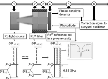
The fundamental concept behind atomic clocks is to exploit an atomic resonance as a reference to stabilize the frequency of a quartz oscillator. In a dr rb atomic clock [1], this resonance is the clock transition between the two ground-state hyperfine levels of rb87, at a microwave fre-quency near 6.83 Ghz (52s
1/2 state, |F = 2, mF = 0〉 to |F = 1, mF = 0〉), detected on atoms maintained in a small rb reference cell, as shown in Fig. 1. In a dr rb clock, pump light from a lamp or laser resonant with the rb d1 or d2 line (795.0 or 780.2 nm, respectively) illuminates the cell and creates a ground-state polarization in the at-oms. The clock transition is then detected by applying a microwave field to the atoms via a microwave-cavity placed around the cell, and the resonance manifests itself as a narrow dip in pump-light power transmitted through the cell versus microwave frequency. The frequency of a voltage-controlled quartz oscillator is locked to this dip using phase-sensitive detection.
our envisioned dr rb atomic clock is shown in Fig. 2 and consists of a microfabricated rb plasma light source, a micro-fabricated rb85 filter, a micro-fabricated rb refer-ence cell which is enclosed by a miniaturized microwave cavity, and a photodetector. The rb plasma light source intrinsically emits at the correct wavelengths, rb d1 and d2 lines, required for a rb clock.
B. Rb Plasma Light Source
When, after excitation, rb atoms decay from the 52P 1/2, 3/2 states back to the ground state 52s1/2, they radiate the rb d1 and d2 wavelengths used for optical pumping of rb87 atoms in rb atomic clocks. The excitation can be provided by maintaining a sufficiently strong ac electric field across a volume of rb and buffer gas, where
inelas-tic collisions between accelerated electrons and rb or gas atoms result in excitation and impact ionization [16]. The following de-excitations give rise to a plasma glow dis-charge [16] and additional electron-ion pairs created by ionizing collisions to an avalanche process and a sustained glow discharge [17].
designing rb glow discharge lamps for microfabricated clocks involves four important considerations: low power consumption (< a few milliwatts), small size (a few cubic millimeters), a microfabricated planar structure, and long lifetime (several years). conventional inductively coupled spherical lamps with diameters of order 1 cm use one or two external rF coils operated at frequencies typically between 75 and 300 Mhz consuming several watts of trical power (80% for light and 20% as heat) to emit elec-tromagnetic discharges (h-discharges) [18] driven by the changing magnetic flux of the coil [19]. although they are a good choice for compact clocks, they become highly inefficient when miniaturized to chip-scale planar lamps in terms of power requirements (tens of watts) and integra-tion because of the external coil requirements. In prin-ciple, a planar spiral coil can be deposited and patterned to inductively couple the plasma [20], but several hundred milliwatts of power will still be required for operation. dc glow discharges, although straightforward, with relatively simple design requirements for chip-scale clocks, need elec-trodes inside the lamp, allowing electrode erosion during operation and, hence, a shortened lifetime [15], [21]. other coupling techniques for discharge lamps, namely, the mi-crowave [22] and the traveling wave discharges [16] also require high power (from a few watts to several hundreds of kilowatts) and are expensive, with very low efficiency when scaled down to chip-scale sizes [16].
dielectric barrier discharges (dBd) are widely used in plasma display panels and other industrial applications. They are based on the same physics as capacitively cou-pled plasmas (ccP), for which an ac field is used to drive a discharge between metal electrodes [23], but are char-acterized by the presence of one or more insulating lay-ers in the current path or the discharge gap between the electrodes. dBds are an efficient low-power technique to
Fig. 1. operating principle of a dr atomic clock. In the lower part, the level scheme of rb87 is sketched, along with the light emitted (downward
arrows) or absorbed (upward arrows) in the respective cells.
Fig. 2. schematic representation of the envisioned chip-scale dr clock showing a possible chip-stack configuration.
Townsend breakdown regime, generating a diffuse glow discharge, whereas at higher pressures (approximately more than 50 hPa), the discharge generally splits up into a large number of randomly distributed microdischarges or current filaments of nanosecond duration also called the streamer regime [24], [25]. In both regimes, the di-electric barrier serves two functions: 1) it distributes the microdischarges evenly over the entire electrode area and 2) it limits the amount of charge and energy that can be fed into an individual microdischarge. after typically a few nanoseconds, the microdischarge is choked because of charge build up on the dielectric, which results in a lo-cal reduction of the electric field within the filament [23]. Typically an electric field of few hundred volts per meter is required to sustain a visible glow discharge in these con-ditions; however, the breakdown voltage required to ignite the discharge is around several hundred volts depending on gas pressure and discharge gap conditions.
We finally note that the mean energy of the electrons and the short duration of the microdischarges strongly limit any heating of the gas atoms, allowing the major fraction of the energy gained by the electrons in the elec-tric field to be deposited in excited atomic states [25].
III. device Microfabrication
A. Design and Microfabrication
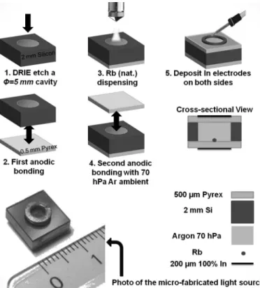
The most important design parameters required to de-velop the rb cell for the rb light source are the discharge gap dimensions, the buffer gas pressure conditions, rb dispensing, cell substrates, and electrodes. To develop a simple microfabrication process flow for this device, in-tended for integration with the envisioned chip-stack clock configuration, silicon (relative electrical permittivity 11.68) was chosen as the cell-wall substrate. Transparent Pyrex (corning Inc., corning, ny) was chosen for the cell lids on both sides because: 1) it can be anodically bonded with si to create a hermetic seal, and 2) it is inert with rb. The chip’s lateral dimensions are chosen to be 1 × 1 cm to integrate with the other 1 × 1 cm components to form a uniform chip-stack.
rb vapor density is very low at room temperature (~10−6 hPa of vapor pressure at 30°c), and can be in-creased by increasing the cell temperature (e.g., to
duce the ratio of rb spectral lines to that of the buffer gas for a given input power, thus lowering the yield for the rb light. hence, following these guidelines and the working regimes of dBds, a configuration with two different rb cells with 70 hPa ar and 30 hPa ar and a discharge gap of 2 mm was chosen (2-mm-thick si cell wall with 500-μm-thick Pyrex cell lids). The (pd) products of the cells are 14 and 6 Pa·m, both well within the range of good starting parameters for this device. argon was chosen because it is inert to rb, has a relatively smaller diameter, and higher mean free path among noble gases, with an ionization po-tential of 15.75 eV [17].
The micro-fabricated rb cell (height: 0.3 cm), consists of a stack of three layers: Pyrex (500 μm thick), silicon (2 mm thick), Pyrex (500 μm thick) which enclose a 5-mm-diameter, 2-mm-thick cylindrical cavity in which a few micrograms of rubidium and the desired pressure of argon are hermetically sealed by a two-step anodic bond-ing process (Fig. 3). First, the cavity is created by deep reactive-ion etching (drIE) a through-hole in the silicon wafer. Then, the etched silicon wafer is anodically bonded to the bottom Pyrex layer at 300°c while applying 1000 V between the two layers. after this first bonding step, the natural rb is dispensed into the cavity under vacuum from a commercial rb source. The desired pressure of ar-gon is introduced in the chamber, and the top Pyrex layer is anodically bonded to the bottom layers at 300°c and 400 V (for approximately one hour) to create the hermeti-cally sealed rb vapor cell [29]. a similar process flow was carried out for the rb+ 30-hPa cell as well. These two cells will be referred to as the 70-hPa and 30-hPa cells in this paper.
a 200-μm-thick, 4.5-mm inner diameter, and 5.5-mm outer diameter 100% indium solder ring or film is depos-ited on top of both sides of the Pyrex layers (i.e., outside the cell) to act as capacitive parallel electrodes to couple rF power to the cell. Indium wets glass well and is, hence, a good choice for electrode deposition on the Pyrex walls. The indium (100%) electrodes are deposited by placing and aligning pre-formed indium rings on top of Pyrex lay-ers above the cavity and reflowing using a soldering iron. These external electrodes avoid electrode corrosion and might allow for lower power consumption when compared with the more traditional internal electrode designs [19]. note that in a future wafer-level production of the plas-ma light source, the electrodes can be directly integrated
onto the Pyrex layers by evaporation or sputtering and micropatterning techniques, and could be made of a dif-ferent metal or transparent metal oxide like ITo to bet-ter withstand high temperatures. our micro-discharge cell design is thus compatible with wafer-level manufacturing of many devices at a time, potentially allowing for greatly reduced cost per unit.
B. RF Drive Electronics Circuit
When dBds are ignited in an ac field, high-voltage, low-frequency (<500 khz) operation tends to spread the microdischarges, whereas low-voltage, high-frequency (>500 khz) operation tends to reignite the same microdis-charge channels every half-period [23]. For a given electric field strength, the higher the frequency is, the less kinetic energy the electrons can accumulate during each rF cycle [25], and thus a higher peak voltage is required for plasma ignition at higher frequencies, which can lead to lower power efficiency. In this work, we observed that it was only possible to ignite and sustain a glow discharge within the frequency range of 1 to 36 Mhz, with our equipment hav-ing a maximum rF power of 10 W, despite adapthav-ing the impedance matching circuit for each frequency (see the subsequent discussion).
The microfabricated rb vapor cell—with the patterned In electrodes—has a measured capacitance of ~0.4 pF at frequencies below 10 Mhz and up to ~1.6 pF at higher
frequencies (<36 Mhz), and a reactance of ~j85 kΩ at low frequencies (a few megahertz). In our setup, we use a stan-dard laboratory rF generator (33220a, agilent technolo-gies Inc., santa clara, ca; maximum amplitude: 10 Vpp) with an output impedance of 50 Ω as the signal source, see Fig. 4(a). To transfer power efficiently to the chip, and to reach the high ac voltage required for breakdown, an im-pedance matching circuit is thus required. several circuits based on l-c components were used, an example network is shown in Fig. 4(b). The two main components in the impedance matching network are 1) a capacitor in parallel to the cell to reduce the overall capacitive reactance, and 2) an inductor in series with these capacitors to cancel out the reactive load so as to form a purely resistive load. The values and the equivalent series resistance (Esr) of the components are carefully chosen to maximize the power transfer to the cell.
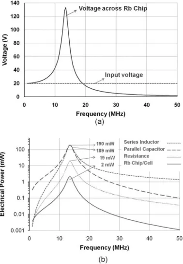
Because the rb chip has a very low capacitance, simple parasitic capacitances become non-negligible for imped-ance matching purposes in the megahertz range. Imped-ance matching was done with the aid of smith charts and a network analyzer, but was made efficient by careful measurements of these parasitic capacitances and includ-ing a variable capacitor in parallel for tuninclud-ing. Fig. 5(a) shows the sPIcE simulation of the voltage amplification
Fig. 3. Microfabrication process flow of the rb light source showing rb dispensing and hermetic sealing for the 70-hPa cell. steps 1 and 2 are performed at wafer level and steps 3 to 5 are completed at chip level. For the 30-hPa cell, the same process flow is used except for the change in ar pressure.
Fig. 4. (a) schematic of the rF circuitry designed for plasma ignition. (b) an example impedance matching network of lcr components for 13.56 Mhz.
achieved across the chip at a desired frequency for the example circuit shown in Fig. 4(b). Fig. 5(b) shows the simulation of power consumed by different circuit com-ponents for a given input signal for the same circuit. It can be seen that nearly 94% of the power is consumed by the series inductor and parallel capacitor, about 5% is consumed by the series resistance, and <1% of the total power is coupled to the chip.
IV. results and discussion
The light source using both the 70-hPa and 30-hPa cells were impedance matched, ignited (Fig. 6), and tested at several drive frequencies over the 1 to 36 Mhz frequen-cy range. The temperature of the rb cell was controlled by a small hotplate thermostat placed under the cell. The results reported in this article (a subset of which were also reported in conference proceedings [30], [31]) were obtained at 4.6 Mhz, where optimal performance of the device was observed.
A. Output Optical Characteristics
The output optical spectrum of the 70-hPa-cell light source and 30-hPa-cell light source were measured using an ocean optics UsB4000 spectrometer (ocean optics Inc., dunedin, Fl) and are shown in Fig. 7(a) and 7(b) respectively. at room temperature, both ar and rb lines are visible with comparable intensity. as the cell tempera-ture is increased, the rb vapor pressure rises rapidly (by a factor of 100 between 35°c and 90°c), and indeed a strong increase in the intensity of the rb d1 lines (795.0 nm) and d2 lines (780.2 nm) is observed. This is similar to the behavior observed by [32] and [33] on their comparably sized rb lamps up to around 120°c. however, the reduc-tion in rb d line intensity resulting from self-absorpreduc-tion, as observed at temperatures <120°c in [32] and [33], is not observed in these cells up to 150°c, as expected because of the higher number density of buffer-gas atoms. With in-creasing cell temperature and inin-creasing emitted rb light intensity, a reduction of the ar line intensity is observed. This effect was experimentally observed to be more promi-nent for the 70-hPa cell [Fig. 8(a)].
The total optical power emitted from the rb chip was 100 μW when 2 mW of electrical power was coupled to the cell (400 mW are supplied to the impedance matching circuit), as shown in Fig. 8(b). The optical power emitted on the rb d2 line emitted was 15 μW at a cell tempera-ture of 150°c. This 70-hPa-cell light source was found to be operating distinctly in the streamer regime with several volume microdischarges spread over the dielectric surface at low frequencies (1 to 3 Mhz) and maintained the same microdischarge channels at higher frequencies (>4 Mhz). More volume discharges were observed as thin channels crossing the discharge gap, the number of microdischarges being proportional to the voltage amplitude. at frequen-cies ≥10 Mhz, the discharge was found to become more homogenous, suggesting that the pre-ionization electron density is large enough to cause appreciable overlap and coalescence of primary avalanche heads and smoothing of space-charge field gradients. The 30-hPa-cell light source,
Fig. 5. (a) Greater than 6× voltage amplification is achieved across the rb chip for the example circuit shown in Fig. 4(b). (b) Power consump-tion of the different electrical components of the circuit showing <1% of the total power consumed by the rb chip.
Fig. 6. Photograph of the rb cell on a printed circuit board connected to LCR components emitting the rb glow discharge when supplied with rF power through a 50-Ω coaxial connection.
on the other hand, was found to operate in the diffuse glow discharge regime (Townsend regime) emitting more of a homogenous surface discharge. Its output spectrum follows the same pattern as for the 70-hPa cell when vary-ing the drive frequency, with an increasvary-ing effect of volume discharges at low frequencies (<2 Mhz). Because of the nanosecond duration of these dBds and limited charge transport and energy dissipation, there was very little gas heating: the outside cell temperature was found to be <60°c after several hours of room-temperature operation.
B. Rb Light Power Stability
The optical power of the rb lines was recorded at a constant rF feed condition for the 70-hPa plasma light source operating at a temperature of 100°c. The short-term (seconds) and long-short-term (hours) variation in optical power was measured, as shown in Fig. 9.
The average short-term fluctuations in optical intensity of the rb lines was found to be less than 0.1% and the
Fig. 7. output optical spectrum of the (a) 70-hPa cell and (b) 30-hPa cell for temperatures from 25°c to 150°c at 600 mW total input rF power.
Fig. 8. (a) comparison of rb and ar line intensity variations with tem-perature in the two cells. (b) output optical power of the 70-hPa cell as a function of cell temperature.
Fig. 9. rb lines stability with time: 70-hPa cell at 100°c and 600 mW rF input power.
long-term variations were found to be less than 5% (shown in Fig. 9). The primary cause of the long-term variations in optical power is the drift in resistance (2 to 3%) of the electrical components of the impedance matching network with time, mainly resulting from thermal effects. residu-al deviations from a perfect correlation between the two curves might well be caused by intensity variations of an ar emission line close to 795 nm that cannot be separated from the rb d1 line with the spectrometer used here. These long-term variations can, in principle, be limited to less than 0.01% using a proportional-integral-deriva-tive (PId) feedback loop that controls the input electrical power and/or the rF drive frequency to maintain a steady output light power level. The short-term fluctuations were observed to have lower amplitudes at higher frequencies (>8 Mhz) and higher amplitudes at low frequencies result-ing from the random distribution of the microdischarges in the streamer regime, in which the same microdischarge channels are not reignited during all half cycles [23], [24]. The 30-hPa cell was found to have much less fluctuation of the rb light power and to emit a constant light power over most of the frequency range, because of the more diffuse glow discharge operation mode.
The plasmas in both cells were ignited several hundred times, and the 70-hPa cell was operated continuously for more than 3 weeks at 100°c, with no degradation. The anodic bonding technique is very robust, and the hermetic seal does not seem to be affected at all by the plasma op-eration, even at high temperatures.
C. Electrical Power Consumption
as shown in Fig. 10 and in agreement with the ar-guments of section III-B, the power required to ignite and sustain a glow discharge increases as the drive fre-quency increases. This is in agreement with the fact that at low frequencies one achieves higher voltage amplifica-tion across the cell because of capacitive coupling. It also partially follows the trend observed by [34], in which the
during operation. although efficiency is recognized as a challenge for ccPs [16], there is room for improvement in our impedance matching circuit.
V. conclusions
a low-power and stable chip-scale rb plasma light source based on dielectric barrier discharge has been dem-onstrated, with good potential for wafer-scale fabrication. The light source emits several milliwatts of optical power at the 780.2- and 795.0-nm rb lines from a 0.3-cm3 chip stack using <6 mW of rF power coupled to the cell (at 1 to 10 Mhz). a successful rb hermetic sealing tech-nique through standard microfabrication processes has been demonstrated. no degradation of the hermetic seal was seen even after several weeks of continuous operation and hundreds of ignitions. The external electrode design implemented eliminates electrode erosion by the plasma, which is the primary lifetime-limiting factor for electrode lamps. The presented plasma light source can be used for hyperfine optical pumping of rb in novel realizations of atomic devices, such as miniature atomic magnetometers, or when combined with a microfabricated rb85 filter cell [14] in miniature atomic clocks.
acknowledgments
We thank our group members for their support and help.
references
[1] F. droz, P. rochat, G. Barmaverain, M. Brunet, J. delporte, J.-F. dutrey, J.-F. Emma, T. Pike, and U. schmidt, “on-board Galileo raFs, current status and performances,” in Proc. 2003 IEEE Int.
Frequency Control Symp. jointly with the European Frequency and Time Forum, 2003, pp. 105–108.
[2] J. camparo, “The rubidium atomic clock and basic research,” Phys.
Today, vol. 60, no. 11, pp. 33–39, 2007.
[3] s. Knappe, “MEMs atomic clocks,” in Comprehensive Microsystems, vol. 3, amsterdam, The netherlands: Elsevier, 2007, pp. 571–612. [4] r. lutwak, “The chip-scale atomic clock—recent developments,”
in Proc. 2009 IEEE Int. Frequency Control Symp. jointly with the
European Frequency and Time Forum, 2009, pp. 573 – 577.
[5] W. E. Bell, a. l. Bloom, and J. lynch, “alkali metal vapor spectral lamps,” Rev. Sci. Instrum., vol. 32, no. 6, pp. 688–692, 1961. Fig. 10. Electrical power consumption of the cell and circuit versus input
[6] s. Knappe, V. shah, P. schwindt, l. holberg, J. Kitching, l. liew, and J. Moreland, “a microfabricated atomic clock,” Appl. Phys.
Lett., vol. 85, no. 9, pp. 1460–1462, 2004.
[7] a. M. Braun, T. J. davis, M. h. Kwakernaak, J. J. Michalchuk, a. Ulmer, W. K. chan, J. h. abeles, Z. a. shellenbarger, y. y. Jau, W. happer, T. Mcclelland, h. Fruehauf, r. drap, W. Weidemann, and M. Variakojis, “rF-interrogated end-state chip-scale atomic clock,” Proc. 39th Annu. Precise Time and Time Interval Meeting, 2007, pp. 233–247.
[8] l.-a. liew, s. Knappe, J. Moreland, h. robinson, l. hollberg, and J. Kitching, “Microfabricated alkali atom vapor cells,” Appl. Phys.
Lett., vol. 84, no. 14, pp. 2694–2696, 2004.
[9] a. douahi, l. nieradko, J. c. Beugnot, J. dziuban, h. Maillote, s. Guerandel, M. Moraja, c. Gorecki, and V. Giordano, “Vapour microcell for chip scale atomic frequency standard,” Electron. Lett., vol. 43, no. 5, pp. 279–280, 2007.
[10] F. Vecchio, V. Venkatraman, h. shea, T. Maedar, and P. ryser, “dispensing and hermetic sealing rb in a miniature reference cell,”
Sens. Actuators A, vol. 172, no. 1, pp. 330–335, 2011.
[11] y. Pétremand, c. schori, r. straessle, G. Mileti, n. de rooij, and P. Thomann, “low temperature indium-based sealing of microfab-ricated alkali cells for chip scale atomic clocks,” in Proc. European
Frequency and Time Forum, noordwijk, The netherlands, 2010, p.
119.
[12] K. Tsujimoto, y. hirai, K. sugano, T. Tsuchiya, and o. Tabata, “sacrificial microchannel sealing by glass-frit reflow for chip scale atomic magnetometer,” in Proc. IEEE 24th Int. Conf. MEMS, can-cun, Mexico, 2011, pp. 368–371.
[13] h. Guo and a. lal, “self-powered photon source,” in IEEE Proc.
12th Int. Conf. Solid State Sensors, Actuators and Microsystems,
2003, pp. 1474–1477.
[14] s. Wang, l. lin, and h. Guo, “analysis and design of a microma-chined rb85 filter in passive rubidium atomic clock,” in Proc. IEEE
Int. Conf. Nano/Micro Engineered and Molecular Systems, 2009, pp.
911–914.
[15] P. carazzetti, P. renaud, and h. shea, “Micromachined chip-scale plasma light source,” Sens. Actuators A, vol. 154, no. 2, pp. 275–280, 2009.
[16] a. Bogaerts, E. neyts, r. Gijbels, and J. van der Mullen, “Gas discharge plasmas and their applications,” Spectrochim. Acta B, vol. 57, pp. 609–658, 2002.
[17] E. nasser, Fundamentals of Gaseous Ionization and Plasma
Electron-ics. new york, ny: Wiley-Interscience, 1971.
[18] G. Babat, “Electrodeless discharges and some allied problems,” J.
Inst. Electr. Eng. Part III: Radio Commun. Eng., vol. 94, no. 27, pp.
27–37, 1947.
[19] d. o. Wharmby, “Electrodeless lamps for lighting: a review,” Proc.
Inst. Electr. Eng., vol. 140, pp. 465–473, 1993.
[20] J. a. hopwood, “a microfabricated inductively coupled plasma gen-erator,” J. Microelectromech. Syst., vol. 9, no. 3, pp. 309–313, 2000. [21] r. G. longwitz, “study of gas ionization in a glow discharge and
development of a micro gas ionizer for gas detection and analysis,” Ph. d. thesis, Institute of Microsystems and Microelectronics, Ecole Polytechnique Federale de lausanne, 2004.
[22] c. M. Ferreira and M. Moisan, Microwave Discharges, Fundamentals
and Applications (naTo asI series, series B: Physics, vol. 302),
new york, ny: springer-Verlag, 1993.
[23] U. Kogelschatz, B. Eliasson, and W. Egli, “dielectric barrier dis-charges. Principle and applications,” J. Phys. IV, vol. 7, no. c4, pp. 447–466, 1997.
[24] r. a. siliprandi, h. E. roman, r. Barni, and c. riccardi, “charac-terization of the streamer regime in dielectric barrier discharges,” J.
Appl. Phys., vol. 104, no. 6, art. no. 063309, 2008.
[25] B. Gellert and U. Kogelschatz, “Generation of excimer emission in dielectric barrier discharges,” Appl. Phys. B, vol. 42, no. 1, pp. 14–21, 1991.
[26] F. Paschen, “Über die zum funkenübergang in luft, wasserstoff und kohlensäure bei verschiedenen drücken erforderliche potentialdiffer-enz,” Ann. Phys., vol. 37, no. 5, pp. 69–75, 1889. (in German) [27] K. c. choi, G. F. saville, and s. c. lee, “Microbridge plasma
dis-play panel with high gas pressure,” IEEE Trans. Electron Devices, vol. 45, no. 6, 1998.
[28] T. akiyama, “Evaluation of discharge cell structure for color ac plasma display panels,” in Proc. 15th Int. Display Res. Conf., 1995, pp. 377–380.
[29] J. diFrancesco, F. Gruet, c. schori, c. affolderbach, r. Matthey, G. Mileti, y. salvadé, y. Petremand, and n. de rooij, “Evaluation
of the frequency stability of a VcsEl locked to a micro-fabricated rubidium vapour cell,” Proc. SPIE, vol. 7720, art. no. 77201T, 2010. [30] V. Venkatraman, y. Petremand, c. affolderbach, G. Mileti, n. de
rooij and h. shea, “Microfabrication and packaging of a rubidium vapor cell as a plasma light source for MEMs atomic clocks,” in
Proc. Transducers 2011, pp. 1907–1910.
[31] V. Venkatraman, y. Petremand, c. affolderbach, G. Mileti, n. de rooij, and h. shea, “low-power chip-scale rubidium plasma light source for miniature atomic clocks,” in Proc. Int. Frequency Control
Symp.–European Frequency and Time Forum 2011, pp. 1–4.
[32] h. Fukoyo, K. Iga, n. Kuramochi, and h. Tanigawa, “Temperature dependence of hyperfine spectrum of rb d1 line,” Jpn. J. Appl.
Phys., vol. 9, no. 7, pp. 729–734, 1970.
[33] J. c. camparo and r. Mackay, “spectral mode changes in an alkali rF discharge,” J. Appl. Phys., vol. 101, no. 5, art. no. 053303, 2007. [34] J. l. Walsh, y. T. Zhang, F. Iza, and M. G. Kong, “atmospheric-pressure gas breakdown from 2 to 100 Mhz,” Appl. Phys. Lett., vol. 93, no. 23, art. no. 221505, 2008.
Vinu Venkatraman received his B.E. (honors)
degree in electrical and electronics and M.sc. (honors) degree in chemistry from the Birla Insti-tute of Technology and science, Pilani, India, in 2006 and an M.s. degree in electrical engineering from Portland state University, Portland, or, in 2008.
since 2009, he has been pursuing his Ph.d. de-gree at the Microsystems for space Technologies laboratory, EPFl, switzerland.
Yves Pétremand received the Ph.d. degree
from the Institute of Microtechnology of the Uni-versity of neuchâtel, switzerland, in 2008.
since June 2008, he has been working at EPFl, switzerland, as a scientist. his major re-search interests include microfabrication gies for various applications, especially technolo-gies based on silicon bulk micromachining.
Christoph Affolderbach received his diploma
and Ph.d. degrees, both in physics, from Bonn University, Germany, in 1999 and 2002, respec-tively. From 2001 to 2006, he was a research scien-tist at the observatoire cantonal de neuchâtel, neuchâtel, switzerland. In 2007, he joined the laboratoire Temps-Fréquence at the University of neuchâtel, neuchâtel, switzerland as scientific collaborator.
his research interests include the development of stabilized diode laser systems, atomic spectros-copy, and vapor-cell atomic frequency standards, in particular laser-pumped high-performance atomic clocks and miniaturized frequency standards.
Gaetano Mileti received his engineering degree
in physics from the swiss Federal Institute of Technology, lausanne, switzerland, in 1990 and the Ph.d. degree in physics from the neuchâtel University, neuchâtel, switzerland, in 1995. From 1991 to 1995 and from 1997 to 2006, he was a re-search scientist at the observatoire cantonal de neuchâtel. From 1995 to 1997, he was a guest sci-entist at the national Institute of standards and Technology, Boulder, co.
In 2007, he co-founded the laboratoire Temps-Fréquence (lTF) at the University of neuchâtel, where he is deputy director and head of research. his research interests include atomic spec-troscopy, stabilized lasers, and frequency standards.
for “pioneering contributions to microsystem technology and effective